US5124875A - Overcurrent protection apparatus - Google Patents
Overcurrent protection apparatus Download PDFInfo
- Publication number
- US5124875A US5124875A US07/568,863 US56886390A US5124875A US 5124875 A US5124875 A US 5124875A US 56886390 A US56886390 A US 56886390A US 5124875 A US5124875 A US 5124875A
- Authority
- US
- United States
- Prior art keywords
- output
- rectifier
- voltage
- current
- reference voltage
- Prior art date
- Legal status (The legal status is an assumption and is not a legal conclusion. Google has not performed a legal analysis and makes no representation as to the accuracy of the status listed.)
- Expired - Fee Related
Links
Images



Classifications
-
- H—ELECTRICITY
- H02—GENERATION; CONVERSION OR DISTRIBUTION OF ELECTRIC POWER
- H02H—EMERGENCY PROTECTIVE CIRCUIT ARRANGEMENTS
- H02H3/00—Emergency protective circuit arrangements for automatic disconnection directly responsive to an undesired change from normal electric working condition with or without subsequent reconnection ; integrated protection
- H02H3/08—Emergency protective circuit arrangements for automatic disconnection directly responsive to an undesired change from normal electric working condition with or without subsequent reconnection ; integrated protection responsive to excess current
-
- H—ELECTRICITY
- H02—GENERATION; CONVERSION OR DISTRIBUTION OF ELECTRIC POWER
- H02H—EMERGENCY PROTECTIVE CIRCUIT ARRANGEMENTS
- H02H1/00—Details of emergency protective circuit arrangements
- H02H1/06—Arrangements for supplying operative power
- H02H1/063—Arrangements for supplying operative power primary power being supplied by fault current
- H02H1/066—Arrangements for supplying operative power primary power being supplied by fault current and comprising a shunt regulator
Definitions
- the present invention relates generally to an overcurrent protection apparatus, and more particularly to an overcurrent protection apparatus which is combined with a circuit breaker.
- FIG. 7 illustrates a circuit diagram of an overcurrent protection apparatus in the prior art shown in the U.S. Pat. No. 3,818,275.
- an electric line 1 is connected to a power source line 1A of an alternating current through a switch F of a circuit breaker 2.
- the current IL of the electric line 1 is detected by a current transformer 4 (hereinafter abbreviated as CT).
- CT4 current transformer 4
- the output of the CT4 is rectified by a full wave bridge rectifier circuit 5, and a DC voltage is output from terminals 5A and 5B.
- a series connection of a resistor 6 and a control circuit 7 is coupled across the terminals 5A and 5B through a resistor 5C.
- the control circuit 7 is composed of two transistors 7A and 7b which have their collectors cupled to the resistor 6 and a Zener diode.
- the emitter of the transistor 7A is coupled to the base of the transistor 7B through a Zener diode 7C which is connected to the emitter of the transistor 7A at the cathode.
- the emitter of the transistor 7B is coupled to the terminal 5B.
- Another zener diode 8 is coupled between the junction 5D between the resistors 5C and 6 and the base of the transistor 7B in a manner that the cathode of the zener diode 8 is connected to the junction 5D.
- the base of the transistor 7A is connected to an input of a timing circuit 9.
- the zener diode 8 serves to limit the voltage of the junction 5D to a predetermined voltage which is determined by the zener voltage of the zener diode 8.
- the timing circuit 9 is coupled across the junction 5D and the terminal 5B, from which the electric power is supplied to the timing circuit 9.
- a series connection of a trip magnet 3 and a thyristor 10 is coupled across the junction 5D and the terminal 5B in a manner that the cathode of the thyristor 10 is connected to the terminal 5B.
- the gate of the thyristor 10 is connected to the output of the timing circuit 9.
- a capacitor C is coupled between the junction 5D and the input 7D of the timing circuit 9.
- the current IL flowing in the electric line 1 is detected by the CT4.
- An output of the CT4 is rectified by the full wave bridge rectifier 5, and a DC voltage is output at both of the terminals 5A and 5B.
- the DC voltage across the junction 5D and the terminal 5B is lower than the zener voltage of the zener diode 8, so that no current flows through the zener diode 8.
- the voltage across the input 7D and the terminal 5B is held at a constant value which is determined by the zener voltage of the zener diode 7C.
- the voltage across the junction 5D and the input 7D varies in response to the current IL in the electric line 1, since the current which flows through the resistor 6 and the control circuit 7 varies. Consequently, electric power consumption in the resistor 6 and the control circuit 7 varies, wherein most of the electric power in the control circuit 7 is consumed in the zener diode 7C.
- the voltage across the junction 5D and the input 7D exceeds a predetermined threshold voltage of the timing circuit 9, which activates the timing circuit 9.
- the output is applied to the gate of the thyristor 10, and the thyristor 10 turns ON. Hence, the trip coil 3 of the circuit breaker 2 is excited and the switch F is opened.
- An object of the present invention is to provide an overcurrent protection apparatus which is improved in electric power consumption.
- the overcurrent protection apparatus in accordance with the present invention comprises:
- a current transformer for detecting a current of an alternating current electric line
- a reference voltage generator for generating a predetermined reference voltage
- duty ratio varying means for generating a control signal for varying a duty ratio of operation of the switching means in proportion to the output voltage of the rectifier in an output voltage range which exceeds the reference voltage
- circuit breaker means for disconnecting the alternating current electric line from an electric power source line when a voltage across the resistor exceeds a predetermined value.
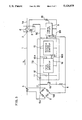
- FIG. 1 is a circuitry of a first protection apparatus in accordance with the present invention that includes a comparator
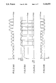
- FIGS. 2(a), 2(b), 2(c) and 2(d) are waveforms in operation of the first protection apparatus
- FIG. 3 is a circuitry of a second protection apparatus in accordance with the present invention that includes a pulse signal generator
- FIGS. 4(a), 4(b) and 4(c) are waveforms in operation of the second protection apparatus
- FIG. 5 is a circuitry of a third protection apparatus in accordance with the present invention that includes first and second pulse signal generators connected to plural reference voltage generators;
- FIG. 6 is a circuitry of a fourth protection apparatus in accordance with the present invention that includes a pulse signal generator and plural current transformers connected to rectifiers;
- FIG. 7 is the circuitry of the overcurrent protection apparatus in the prior art.
- FIG. 1 is a circuit diagram of a first embodiment of the overcurrent protecting apparatus in accordance with the present invention.
- an electric line 1 is connected to a power source line 1A of an alternating current through a switch F of a circuit breaker 2.
- a current IL in the electric line 1 is detected by a current transformer 4.
- the output of the current transformer 4 is rectified by a full wave bridge rectifier 5.
- a series connection of a transistor 15 and a resistor 6 is coupled across a positive terminal 5A and a negative terminal 5B of the rectifier 5.
- a control circuit 7A is coupled in parallel to the transistor 15.
- a timing circuit 9 is coupled across a positive power source line 5C and a negative power source line 9B of the control circuit. The timing circuit 9 is activated when the absolute value of a negative input voltage V3 across the negative power source line 9B and the negative terminal 5B exceeds a predetermined voltage VT. The delay time of the timing circuit 9 varies in compliance with the negative input voltage V3.
- the timing circuit 9 is provided with a filter circuit therein, which filters the pulsating input voltage V3.
- the output 9A of the timing circuit 9 is connected to the gate of a switch means or a thyristor 10.
- the thyristor 10 turns ON when the timing circuit 9 finishes a time counting operation.
- a trip coil 3 of the circuit breaker 2 is connected between the positive power source line 5C and the anode of the thyristor 10, and is excited by conductive state of the thyristor 10.
- the switch F is disconnected by the excitation of the trip coil 3.
- a diode 11 interrupts a current flow from the positive power source line 5C to the positive terminal 5A.
- a capacitor 12 serves as a filter.
- a reference voltage generator 13 generates a predetermined reference voltage.
- the reference voltage is applied to the invert input (-) of a comparator 14.
- the voltage V1 at the line 5C is divided into a suitable voltage V2 by a dividing network of resistors R1 and R2.
- the voltage V2 is applied to the noninvert input (+) of the comparator 14.
- the output of the comparator 14 is applied to the base of the transistor 15.
- FIGS. 2(a), 2(b), 2(c) and 2(d) are waveforms in operation of the first embodiment.
- a current IL in the electric line 1 is detected by the current transformer 4, and the output of the current transformer 4 is rectified by the rectifier 5.
- the waveform of the output current I1 from the positive terminal 5A and to the negative terminal 5B of the rectifier 5 is shown in FIG. 2(a).
- the output current I1 flows into the line 5C through the diode 11.
- the waveform of the voltage V2 is shown in FIG. 2(b).
- the reference voltage VR of the reference voltage generator 13 is shown by an alternate long and short dash line.
- a voltage Vb which is lower than the voltage VR is also shown by alternate long and two short dashes line.
- the voltage V2 is lower than the reference voltage VR.
- the comparator 14 supplies an output to the base of the transistor 15. Consequently, the transistor 15 turns ON as shown in FIG. 2(c), and the positive terminal 5A is short-circuited with the line 9B.
- the electric charge in the capacitor 12 is the discharged by current consumption in the comparator 14, reference voltage generator 13, timing circuit 9 and resistors R 1 and R 2 , and the voltage V2 gradually falls.
- the output of the comparator disappears, and the transistor 15 turns OFF. Therefore, the current in the transistor 15 and the resistor 6 disappears, and the voltage at the point 5A rises.
- the above-mentioned operation is repeated, and the voltage V2 is limited to a voltage which is not so higher than the reference voltage VR. Consequently, a duty ratio in operation of the transistor 15 is varied in compliance with the voltage across the terminals 5A and 5B.
- an increase of the voltage V1 is limited by short-circuiting the terminal 5A and the line 9B from which an electric power is supplied to the control circuit 7A.
- the electric power consumption in the control circuit 7 is comparatively low because the reference voltage generator 13 and the comparator are composed of electronic circuits which consume little electric power. Therefore, the current flowing in the resistor 6 is comparatively lower, and the electric power consumption in the resistor 6 is comparatively lower in short-circuit state of the terminal 5A and the line 9B by the conductive state of the transistor 15. Hence, a small size resistor can be used.
- FIG. 3 illustrates a circuit diagram of a second embodiment of the overcurrent protection circuit in accordance with the present invention.
- the comparator 14 in the first embodiment is replaced with a pulse signal generator 16.
- the remaining components function in the same manner as described in the first embodiment and are designated by like numerals as used with corresponding parts shown in FIG. 1, and therefore will not be described.
- the pulse signal generator 16 generates a square wave signal of which a duty ratio is varied in compliance with an input voltage which is applied to a terminal 16A thereof.
- the reference voltage VR is applied to the other input terminal 16B.
- FIG. 4(a) is a waveform of an output of the rectifier 5.
- FIG. 4(b) is a waveform of a voltage V1 across the lines 5C and 9B
- FIG. 4(c) is a diagram for representing switching operation of the transistor 15.
- the diagram of shown in FIG. 4(c) is substantially identical to the waveform of the output of the pulse signal generator 16, but the cycle period of the switching operation is shorter than that of the first embodiment, and the duty ratio of the output of the pulse signal generator 16 is increased in proportion to the increase of the output voltage of the rectifier 5.
- the capacitance of the filter capacitor 12 can be reduced.
- FIG. 5 illustrates a circuits diagram of a third embodiment of the overcurrent protection apparatus in accordance with the present invention.
- a timing circuit 29 is provided with two input terminals 29A and 29B for receiving differential inputs.
- a positive input Vc is applied across a positive power input terminal connected to the line 5C and the input terminal 29A
- a negative input Vd is applied across a negative power input terminal connected to the line 9B and the input terminal 29A.
- the input terminal 29B is connected to the negative terminal 5B of the rectifier 5.
- Two control circuits 7B and 17 are provided for supplying the positive inputs Vc and negative input Vd, respectively.
- Transistors 15 and 21 are coupled to the control circuits 7B and 17, respectively.
- the timing circuit 29 since the timing circuit 29 is activated by the differential input, the accuracy in the detection of an overcurrent is improved.
- FIG. 6 illustrates a circuit diagram of a fourth embodiment in accordance with the present invention.
- two current transformers 4 and 23 are coupled to the electric line 1.
- the output terminals 4A and 4B of the current transformer 4 are short-circuited by a switch 25.
- the output of the current transform 4 is rectified by the full wave bridge rectifier 5 and is applied to a control circuit 7C.
- the control circuit 7C is identical with the control circuit 7B shown in FIG. 3 with the exception of the diode 11.
- the switch 25 is controlled by the output of the pulse signal generator 16.
- the output of the other current transformer 23 is also rectified by the other full wave bridge rectifier 24.
- a resistor 26 is coupled across the DC output terminals 24A and 24B, and the DC output voltage is applied to the input of the timing circuit 9.
- the control circuit 7C serves to supply the electric power to the timing circuit 9.
- the switch 25 is connected or disconnected by the output of the pulse signal generator 16, and the DC voltage across the terminals 5A and 5B is held to a predetermined constant value.
- the DC voltage across the terminals 24A and 24B of the rectifier 24 varies in proportion to the variation of the current IL of the electric line 1.
- the timing circuit 9 is activated, and the operation of the switch 10 and the circuit breaker 2 follows in a manner similar to that described in the first embodiment.
- the output of the current transformer 23 is used to activate only the timing circuit 9. Therefore, power consumption can be disregarded. Consequently, linearity in current detection of the current transformer 25 is improved, and accuracy in overcurrent detection is also improved.
- the current protection apparatus in accordance with the present invention can be applicable to a plurality of electric lines.
Landscapes
- Engineering & Computer Science (AREA)
- Power Engineering (AREA)
- Emergency Protection Circuit Devices (AREA)
Applications Claiming Priority (2)
| Application Number | Priority Date | Filing Date | Title |
|---|---|---|---|
| JP1257876A JPH0710145B2 (ja) | 1989-10-04 | 1989-10-04 | 過電流保護装置 |
| JP1-257876 | 1989-10-04 |
Publications (1)
| Publication Number | Publication Date |
|---|---|
| US5124875A true US5124875A (en) | 1992-06-23 |
Family
ID=17312410
Family Applications (1)
| Application Number | Title | Priority Date | Filing Date |
|---|---|---|---|
| US07/568,863 Expired - Fee Related US5124875A (en) | 1989-10-04 | 1990-08-17 | Overcurrent protection apparatus |
Country Status (6)
| Country | Link |
|---|---|
| US (1) | US5124875A (ja) |
| EP (2) | EP0687050A3 (ja) |
| JP (1) | JPH0710145B2 (ja) |
| KR (1) | KR910008905A (ja) |
| DE (1) | DE69028171T2 (ja) |
| ZA (1) | ZA906490B (ja) |
Cited By (14)
| Publication number | Priority date | Publication date | Assignee | Title |
|---|---|---|---|---|
| US6813124B1 (en) * | 2002-06-21 | 2004-11-02 | Lionel L.L.C. | Transformer over-current protection with RMS sensing and voltage fold-back |
| US20050201033A1 (en) * | 2004-03-09 | 2005-09-15 | Samsung Measuring Instruments Co., Ltd. | Apparatus for monitoring open state of the secondary terminals of a current transformer |
| US20050207075A1 (en) * | 2002-08-02 | 2005-09-22 | Protectelec Pty Limited | Control circuit and a method for electrically connecting a load to a power source |
| US20080012667A1 (en) * | 2006-07-14 | 2008-01-17 | Square D Company | Method and system for time synchronized trip algorithms for breaker self protection |
| US20080012668A1 (en) * | 2006-07-14 | 2008-01-17 | Square D Company | Redundant trip activation |
| US20080012670A1 (en) * | 2006-07-14 | 2008-01-17 | Square D Company | Switch-to-trip point translation |
| US20080012666A1 (en) * | 2006-07-14 | 2008-01-17 | Square D Company | Method and system of current transformer output magnitude compensation in a circuit breaker system |
| US20080013235A1 (en) * | 2006-07-14 | 2008-01-17 | Square D Company | Redundant instantaneous trip detection |
| US20080012669A1 (en) * | 2006-07-14 | 2008-01-17 | Square D Company | Burden resistor temperature compensation algorithm |
| US20080012677A1 (en) * | 2006-07-14 | 2008-01-17 | Squara D Company | Circuit breaker-like apparatus with combination current transformer |
| US20080013238A1 (en) * | 2006-07-14 | 2008-01-17 | Square D Company | Low cost user adjustment, resistance to straying between positions, increased resistance to ESD, and consistent feel |
| US20080048624A1 (en) * | 2006-07-14 | 2008-02-28 | Square D Company | Method and system of fault powered supply voltage regulation |
| US20080081511A1 (en) * | 2006-06-30 | 2008-04-03 | Molex Incorporated | Low profile latching connector and pull tab for unlatching same |
| US7788055B2 (en) | 2006-07-14 | 2010-08-31 | Square D Company | Method and system of calibrating sensing components in a circuit breaker system |
Families Citing this family (10)
| Publication number | Priority date | Publication date | Assignee | Title |
|---|---|---|---|---|
| FR2699016B1 (fr) * | 1992-12-04 | 1995-01-06 | Simplex Appareils | Ensemble d'alimentation auxiliaire pour poste électrique. |
| DE19641185C2 (de) * | 1996-09-24 | 1998-07-23 | Siemens Ag | Schaltungsanordnung zur Stromerfassung in Stromleitern zur Ansteuerung elektronisch steuerbarer Auslöseeinrichtungen |
| DE19641183C2 (de) * | 1996-09-24 | 1998-08-20 | Siemens Ag | Schaltungsanordnung zur Stromerfassung eines Stromleiters zur Ansteuerung elektronisch steuerbarer Auslöseeinrichtungen |
| DE19641187C2 (de) * | 1996-09-24 | 1998-07-23 | Siemens Ag | Schaltungsanordnung zur Energieversorgung von elektronischen Auslöseeinrichtungen |
| DE19738696A1 (de) * | 1997-08-29 | 1999-03-04 | Siemens Ag | Schaltungsanordnung zur Speisung eines Auslösemagneten eines Leistungsschalters |
| JP2003050637A (ja) * | 2001-08-07 | 2003-02-21 | Mitsubishi Electric Corp | 電源装置 |
| DE102005031833B4 (de) * | 2005-07-06 | 2017-01-05 | Phoenix Contact Gmbh & Co. Kg | Verfahren und elektronische Stromversorgungsvorrichtung zur Energieversorgung einer durch eine Schutzeinrichtung gesicherten Niederspannungslast |
| CN106026656B (zh) * | 2016-07-08 | 2019-01-25 | 上海电科电器科技有限公司 | 迟滞型电源电路 |
| CN107528291A (zh) * | 2017-09-28 | 2017-12-29 | 苏州威利仕塑胶电子有限公司 | 一种过欠电流控制器 |
| US10811185B2 (en) | 2018-09-13 | 2020-10-20 | Analog Devices Global Unlimited Company | Saturation prevention of current transformer |
Citations (3)
| Publication number | Priority date | Publication date | Assignee | Title |
|---|---|---|---|---|
| US3818275A (en) * | 1973-01-30 | 1974-06-18 | Westinghouse Electric Corp | Circuit interrupter including improved trip circuit using current transformers |
| US4331999A (en) * | 1980-04-15 | 1982-05-25 | Westinghouse Electric Corp. | Circuit interrupter with digital trip unit and power supply |
| US4603336A (en) * | 1984-04-25 | 1986-07-29 | Harris Graphics Corporation | Transfer mechanism for multiple station imaging/printing apparatus |
Family Cites Families (5)
| Publication number | Priority date | Publication date | Assignee | Title |
|---|---|---|---|---|
| FR2052906B2 (ja) * | 1969-06-20 | 1975-08-22 | Comp Generale Electricite | |
| US3846675A (en) * | 1973-01-30 | 1974-11-05 | Westinghouse Electric Corp | Molded case circuit breakers utilizing saturating current transformers |
| CH558098A (de) * | 1973-11-27 | 1975-01-15 | Sprecher & Schuh Ag | Schaltungsanordnung zur speisung elektronischer schutzrelais. |
| US4351012A (en) * | 1980-04-15 | 1982-09-21 | Westinghouse Electric Corp. | Circuit interrupter with digital trip unit and means to enter trip settings |
| US4567540A (en) * | 1983-06-22 | 1986-01-28 | S&C Electric Company | Power supply for a circuit interrupter |
-
1989
- 1989-10-04 JP JP1257876A patent/JPH0710145B2/ja not_active Expired - Lifetime
-
1990
- 1990-07-23 KR KR1019900011162A patent/KR910008905A/ko not_active Withdrawn
- 1990-08-16 ZA ZA906490A patent/ZA906490B/xx unknown
- 1990-08-17 US US07/568,863 patent/US5124875A/en not_active Expired - Fee Related
- 1990-09-20 EP EP95113775A patent/EP0687050A3/en not_active Withdrawn
- 1990-09-20 DE DE69028171T patent/DE69028171T2/de not_active Expired - Lifetime
- 1990-09-20 EP EP90118133A patent/EP0421204B1/en not_active Expired - Lifetime
Patent Citations (3)
| Publication number | Priority date | Publication date | Assignee | Title |
|---|---|---|---|---|
| US3818275A (en) * | 1973-01-30 | 1974-06-18 | Westinghouse Electric Corp | Circuit interrupter including improved trip circuit using current transformers |
| US4331999A (en) * | 1980-04-15 | 1982-05-25 | Westinghouse Electric Corp. | Circuit interrupter with digital trip unit and power supply |
| US4603336A (en) * | 1984-04-25 | 1986-07-29 | Harris Graphics Corporation | Transfer mechanism for multiple station imaging/printing apparatus |
Cited By (27)
| Publication number | Priority date | Publication date | Assignee | Title |
|---|---|---|---|---|
| US6813124B1 (en) * | 2002-06-21 | 2004-11-02 | Lionel L.L.C. | Transformer over-current protection with RMS sensing and voltage fold-back |
| US6873142B2 (en) | 2002-06-21 | 2005-03-29 | Lionel L.L.C. | Transformer over-current protection with RMS sensing and voltage fold-back |
| US20050207075A1 (en) * | 2002-08-02 | 2005-09-22 | Protectelec Pty Limited | Control circuit and a method for electrically connecting a load to a power source |
| US7378761B2 (en) | 2002-08-02 | 2008-05-27 | Protectelec Pty Ltd | Control circuit and a method for electrically connecting a load to a power source |
| US20050201033A1 (en) * | 2004-03-09 | 2005-09-15 | Samsung Measuring Instruments Co., Ltd. | Apparatus for monitoring open state of the secondary terminals of a current transformer |
| US7561396B2 (en) * | 2004-03-09 | 2009-07-14 | Samsung Measuring Instruments Co., LTD | Apparatus for monitoring open state of the secondary terminals of a current transformer |
| US7354292B1 (en) | 2006-06-30 | 2008-04-08 | Molex Incorporated | Low profile latching connector and pull tab for unlatching same |
| US20080081511A1 (en) * | 2006-06-30 | 2008-04-03 | Molex Incorporated | Low profile latching connector and pull tab for unlatching same |
| US20080048624A1 (en) * | 2006-07-14 | 2008-02-28 | Square D Company | Method and system of fault powered supply voltage regulation |
| US20080012667A1 (en) * | 2006-07-14 | 2008-01-17 | Square D Company | Method and system for time synchronized trip algorithms for breaker self protection |
| US20080012677A1 (en) * | 2006-07-14 | 2008-01-17 | Squara D Company | Circuit breaker-like apparatus with combination current transformer |
| US20080013238A1 (en) * | 2006-07-14 | 2008-01-17 | Square D Company | Low cost user adjustment, resistance to straying between positions, increased resistance to ESD, and consistent feel |
| US20080013235A1 (en) * | 2006-07-14 | 2008-01-17 | Square D Company | Redundant instantaneous trip detection |
| US20080012666A1 (en) * | 2006-07-14 | 2008-01-17 | Square D Company | Method and system of current transformer output magnitude compensation in a circuit breaker system |
| US20080012670A1 (en) * | 2006-07-14 | 2008-01-17 | Square D Company | Switch-to-trip point translation |
| US20080012668A1 (en) * | 2006-07-14 | 2008-01-17 | Square D Company | Redundant trip activation |
| US7550939B2 (en) | 2006-07-14 | 2009-06-23 | William Davison | Redundant instantaneous trip detection |
| US20080012669A1 (en) * | 2006-07-14 | 2008-01-17 | Square D Company | Burden resistor temperature compensation algorithm |
| US7592888B2 (en) | 2006-07-14 | 2009-09-22 | Jason Robert Colsch | Low cost user adjustment, resistance to straying between positions, increased resistance to ESD, and consistent feel |
| US7683586B2 (en) | 2006-07-14 | 2010-03-23 | Davison William C | Method and system of fault powered supply voltage regulation |
| US7697250B2 (en) | 2006-07-14 | 2010-04-13 | William Davison | Switch-to-trip point translation |
| US7788055B2 (en) | 2006-07-14 | 2010-08-31 | Square D Company | Method and system of calibrating sensing components in a circuit breaker system |
| US7791849B2 (en) | 2006-07-14 | 2010-09-07 | William Davison | Redundant trip activation |
| US7859802B2 (en) | 2006-07-14 | 2010-12-28 | William Davison | Burden resistor temperature compensation algorithm |
| US7869170B2 (en) | 2006-07-14 | 2011-01-11 | Susan Jean Walker Colsch | Method and system for time synchronized trip algorithms for breaker self protection |
| US7869169B2 (en) | 2006-07-14 | 2011-01-11 | William Davison | Method and system of current transformer output magnitude compensation in a circuit breaker system |
| US8154373B2 (en) | 2006-07-14 | 2012-04-10 | Schneider Electric USA, Inc. | Circuit breaker-like apparatus with combination current transformer |
Also Published As
| Publication number | Publication date |
|---|---|
| KR910008905A (ko) | 1991-05-31 |
| ZA906490B (en) | 1991-06-26 |
| EP0421204A2 (en) | 1991-04-10 |
| JPH0710145B2 (ja) | 1995-02-01 |
| DE69028171D1 (de) | 1996-09-26 |
| JPH03124215A (ja) | 1991-05-27 |
| EP0421204A3 (en) | 1992-04-08 |
| EP0687050A2 (en) | 1995-12-13 |
| EP0421204B1 (en) | 1996-08-21 |
| EP0687050A3 (en) | 1996-05-22 |
| DE69028171T2 (de) | 1997-01-23 |
Similar Documents
| Publication | Publication Date | Title |
|---|---|---|
| EP0421204A2 (en) | An overcurrent protection apparatus | |
| US6169391B1 (en) | Device for converting high voltage alternating current to low voltage direct current | |
| US5808847A (en) | Electronic trip device comprising a power supply device | |
| US4652984A (en) | Self-oscillating power-supply circuit | |
| US4745300A (en) | Two-wire switch | |
| US7095630B2 (en) | Capacitively coupled power supply | |
| US5943225A (en) | Circuit for removing a peak reverse voltage generated from a power supply source | |
| US20090168463A1 (en) | Dc to dc converter | |
| JPH0767328A (ja) | スイッチングレギュレータ電源装置 | |
| KR960003201B1 (ko) | 이상전압 검출 제어장치 | |
| EP0736959A1 (en) | Low dissipation power controller | |
| US4277824A (en) | Start-up circuit | |
| WO2000021176A1 (en) | Method and arrangement for limiting starting current in a power supply | |
| KR19980032713A (ko) | 2개의 와이어 전원 전자스위치 | |
| JPS63501539A (ja) | 低リ−ク交流近接スイッチ回路 | |
| EP1639695A1 (en) | Switch mode power circuit | |
| JP2941513B2 (ja) | 不足電圧引外し装置 | |
| JPH053765B2 (ja) | ||
| SU1381647A1 (ru) | Устройство дл ограничени бросков тока включени однофазного трансформатора | |
| JPS6377383A (ja) | 起動回路 | |
| JPH05316723A (ja) | スイッチング電源装置 | |
| SU1295458A1 (ru) | Устройство дл управлени электромагнитом | |
| GB2124804A (en) | Electrical power supply arrangements | |
| JPH0583944A (ja) | 電源装置 | |
| JPS6321146Y2 (ja) |
Legal Events
| Date | Code | Title | Description |
|---|---|---|---|
| AS | Assignment |
Owner name: MITSUBISHI DENKI KABUSHIKI KAISHA, JAPAN Free format text: ASSIGNMENT OF ASSIGNORS INTEREST.;ASSIGNORS:ISHII, KAZUHIRO;HIROTSUNE, KOUJI;REEL/FRAME:005412/0420 Effective date: 19900803 |
|
| FEPP | Fee payment procedure |
Free format text: PAYOR NUMBER ASSIGNED (ORIGINAL EVENT CODE: ASPN); ENTITY STATUS OF PATENT OWNER: LARGE ENTITY |
|
| FPAY | Fee payment |
Year of fee payment: 4 |
|
| REMI | Maintenance fee reminder mailed | ||
| LAPS | Lapse for failure to pay maintenance fees | ||
| FP | Lapsed due to failure to pay maintenance fee |
Effective date: 20000623 |
|
| STCH | Information on status: patent discontinuation |
Free format text: PATENT EXPIRED DUE TO NONPAYMENT OF MAINTENANCE FEES UNDER 37 CFR 1.362 |