US5159530A - Electronic circuit module with power feed spring assembly - Google Patents
Electronic circuit module with power feed spring assembly Download PDFInfo
- Publication number
- US5159530A US5159530A US07/716,886 US71688691A US5159530A US 5159530 A US5159530 A US 5159530A US 71688691 A US71688691 A US 71688691A US 5159530 A US5159530 A US 5159530A
- Authority
- US
- United States
- Prior art keywords
- array
- conductive
- electronic circuit
- circuit module
- integrated circuit
- Prior art date
- Legal status (The legal status is an assumption and is not a legal conclusion. Google has not performed a legal analysis and makes no representation as to the accuracy of the status listed.)
- Expired - Fee Related
Links
Images


Classifications
-
- H—ELECTRICITY
- H05—ELECTRIC TECHNIQUES NOT OTHERWISE PROVIDED FOR
- H05K—PRINTED CIRCUITS; CASINGS OR CONSTRUCTIONAL DETAILS OF ELECTRIC APPARATUS; MANUFACTURE OF ASSEMBLAGES OF ELECTRICAL COMPONENTS
- H05K7/00—Constructional details common to different types of electric apparatus
- H05K7/02—Arrangements of circuit components or wiring on supporting structure
- H05K7/10—Plug-in assemblages of components, e.g. IC sockets
- H05K7/1053—Plug-in assemblages of components, e.g. IC sockets having interior leads
- H05K7/1061—Plug-in assemblages of components, e.g. IC sockets having interior leads co-operating by abutting
-
- H—ELECTRICITY
- H10—SEMICONDUCTOR DEVICES; ELECTRIC SOLID-STATE DEVICES NOT OTHERWISE PROVIDED FOR
- H10W—GENERIC PACKAGES, INTERCONNECTIONS, CONNECTORS OR OTHER CONSTRUCTIONAL DETAILS OF DEVICES COVERED BY CLASS H10
- H10W40/00—Arrangements for thermal protection or thermal control
- H10W40/40—Arrangements for thermal protection or thermal control involving heat exchange by flowing fluids
- H10W40/47—Arrangements for thermal protection or thermal control involving heat exchange by flowing fluids by flowing liquids, e.g. forced water cooling
Definitions
- the present invention relates generally to LSI (large scale integration) modules, and more specifically to the power feed system of LSI modules.
- the stated object of this invention is achieved by separating the paths of power currents into source and ground terminal sides and using pin connectors for carrying exclusively the currents of one side.
- an electronic circuit module which comprises a ceramic substrate having an array of male connectors arranged thereon to establish contact with external female connectors and conductive layers of power distribution pattern embedded therein and coupled to the male connectors.
- An array of integrated circuit packages are provided, each package including an electrically conductive cap or housing, an integrated circuit chip secured thereto in a thermally conductive relationship and a base plate. The latter includes a conductive pattern connected to the conductive housing.
- Each package establishes source/ground current conduction paths between the conductive pattern and the integrated circuit chip and drain/source current conduction paths between the integrated circuit chip and the layer of the ceramic substrate.
- An array of conductive springs are supported in pressure contact relationship the housings of successive integrated circuit packages to establish source/ground conduction paths between the packages and an external source voltage terminal.
- a cooling means is provided for defining an array of cooling surfaces respectively contacting the housings of the integrated circuit packages in a thermally conductive relationship.
- the conductive springs are supported between first and second lattice structures of crossed bars.
- the first lattice structure is formed of conductive material and defines an array of apertures for positioning the integrated circuit packages therein so that they contact with the cooling surfaces, respectively.
- the second lattice structure is preferably formed of nonconductive material and defines an array of apertures corresponding respectively to the apertures of the first lattice structure for positioning the integrated circuit packages so that they establish electrical contacts with the layers of the insulative substrate.
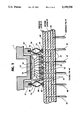
- FIG. 1 is an exploded view, partly in cross-section, of an electronic circuit module of the present invention in relation to a printed circuit board;
- FIG. 2 is a cross-sectional view of the electronic circuit module of the present invention when assembled
- FIG. 3 is an enlarged view in cross-section of a portion of the electronic circuit module of this invention.
- FIG. 4 is a perspective view of a portion of the power feed spring assembly of this invention.
- the electronic circuit module of this invention is generally shown at 3 which is adapted to be used for connection to a printed circuit board 1 by way of a female connector 2 in which an array of contacts 20 is provided.
- Module 3 comprises a male connector assembly 4 having a ceramic substrate 40, an array of ground pins 41 and signal pins 46 juxtaposed on the lower surface of substrate 40, and a ceramic frame 42 in which the substrate 40 is secured.
- An array of LSI packages 5 are provided between the ceramic substrate 40 and a power feed spring assembly 6 that is held in position between the upper edge of frame structure 42 and a cooling device 7 with an insulating spacer 8 interposed therebetween.
- Printed circuit board 1 has conductive layers 10 of power distribution pattern embedded therein, which are suitably connected to the contacts 20 of the female connector with which the pins 41 and 46 of the male connector assembly respectively engage.
- ceramic substrate 40 has conductive layers 43 of power distribution pattern and vertical conducting paths 44 for coupling the layers 43 to the ground pins 41 and further to solder terminals appearing on the upper surface of ceramic substrate 40.
- a signal layer 47 is also buried in the substrate 40 for coupling signal pins 46 to appropriate solder terminals.
- Each of the LSI packages 5 has a base plate 51 and a conductive cap 52.
- An LSI chip 50 is cemented to the ceiling of the conductive cap 52 to establish as high a thermally conductive relationship as possible with the cooling device 7.
- Base plate 51 has embedded conductors 53 which are coupled to the soldering terminals on the ceramic substrate 40 by solder points 45 and coupled to the LSI chip 50 by ground leads 54 and signal leads 58.
- Base plate 51 has a power conductive pattern 55 that is connected by leads 56 to the LSI chip 50.
- Power feed spring assembly 6 comprises a conductive, upper lattice structure 60 of crossed bars 61 defining a rectangular array of square apertures 62.
- Lattice structure 60 has an outer wall portion 69 that extends downwards from the outer edge portions thereof.
- the spring assembly 6 further includes a lower lattice structure 64 of crossed bars 65 defining an array of square apertures 66 corresponding in position to the square apertures 62 of the upper lattice structure.
- Lower lattice structure 64 is formed of insulative material to prevent springs 68 from contacting with soldered conductive surface portions of ceramic substrate 40. As shown in detail in FIG.
- each of the crossed bars 65 of the lower lattice structure is formed with spring alignment holes 67 for supporting and aligning an array of springs 68 of paired bow-like configuration suspending from the upper lattice structure.
- the leaf springs 68 are grouped to form a plurality of sets of three springs each. The upper ends of the springs of each set are firmly secured in a slit provided on the lower side of each crossed bar 61 of the upper lattice structure and their lower ends are engaged in the alignment holes 67 of the lower lattice structure. In this way, springs 68 of each set are aligned parallel with the side walls of adjacent LSI packages 5.
- LSI packages 5, cemented to the ceramic substrate 40 by solder points 45, are moved passing through corresponding apertures 66 of the lower lattice structure against lateral forces of the springs 68 until ceramic substrate 40 bears against the bottom of outer wall portion 63 of the upper lattice structure.
- low impedance electrical paths are established from the upper lattice structure 60 by way of four sets of leaf springs 68 to the conductive cap 52 of each LSI package.
- Thermally conductive but electrically nonconductive material such as grease is applied on the upper surface of each LSI package 5 to form a layer 57 as shown in FIGS. 2 and 3.
- the cooling device 7 has meandering passageways 70 between a coolant inlet 71 and a coolant outlet 72, and defines an array of square-shaped cooling portions 73 corresponding to the apertures 62 of the upper lattice structure.
- the cooling portions 73 are positioned in the corresponding square apertures 62 and establish thermal contact with conductive caps 52 by way of the respective grease layers 57 so that heat generated in LSI chips 50 is efficiently conducted to the cooling device 7.
- the upper lattice structure 60 has portions 69 extending from its four sides beyond the periphery of cooling device 7 to facilitate connection to a power voltage source, not shown. It is seen therefore that source currents applied to the outwardly extending portions 69 of upper lattice structure 60 6 find their passage through bars 61, springs 68, metal caps 52 the conductive pattern 55 embedded in base plate 51 and leads 56 to all LSI chips 50 of the module. Ground currents from all LSI chips are drained through ground leads 54, ground layers 43 and ground pins 41 to printed circuit board 1. Therefore, shorter current paths are achieved with the present invention while allowing an increase in the number of current paths and pin connectors.
Landscapes
- Engineering & Computer Science (AREA)
- Microelectronics & Electronic Packaging (AREA)
- Cooling Or The Like Of Electrical Apparatus (AREA)
- Cooling Or The Like Of Semiconductors Or Solid State Devices (AREA)
- Mounting Of Printed Circuit Boards And The Like (AREA)
- Coupling Device And Connection With Printed Circuit (AREA)
- Multi-Conductor Connections (AREA)
Applications Claiming Priority (2)
| Application Number | Priority Date | Filing Date | Title |
|---|---|---|---|
| JP2-159152 | 1990-06-18 | ||
| JP2159152A JP2518092B2 (ja) | 1990-06-18 | 1990-06-18 | 電子回路モジュ―ル |
Publications (1)
| Publication Number | Publication Date |
|---|---|
| US5159530A true US5159530A (en) | 1992-10-27 |
Family
ID=15687403
Family Applications (1)
| Application Number | Title | Priority Date | Filing Date |
|---|---|---|---|
| US07/716,886 Expired - Fee Related US5159530A (en) | 1990-06-18 | 1991-06-18 | Electronic circuit module with power feed spring assembly |
Country Status (5)
| Country | Link |
|---|---|
| US (1) | US5159530A (de) |
| EP (1) | EP0462552B1 (de) |
| JP (1) | JP2518092B2 (de) |
| CA (1) | CA2044747C (de) |
| DE (1) | DE69108302T2 (de) |
Cited By (8)
| Publication number | Priority date | Publication date | Assignee | Title |
|---|---|---|---|---|
| US5309318A (en) * | 1992-04-21 | 1994-05-03 | International Business Machines Corporation | Thermally enhanced semiconductor chip package |
| US5315239A (en) * | 1991-12-16 | 1994-05-24 | Hughes Aircraft Company | Circuit module connections |
| US6081026A (en) * | 1998-11-13 | 2000-06-27 | Fujitsu Limited | High density signal interposer with power and ground wrap |
| US6239485B1 (en) | 1998-11-13 | 2001-05-29 | Fujitsu Limited | Reduced cross-talk noise high density signal interposer with power and ground wrap |
| US20030024735A1 (en) * | 2001-08-01 | 2003-02-06 | Volker Strutz | Protective device for subassemblies and method for producing a protective device |
| US6594153B1 (en) * | 2000-06-27 | 2003-07-15 | Intel Corporation | Circuit package for electronic systems |
| US6687126B2 (en) * | 2001-04-30 | 2004-02-03 | Hewlett-Packard Development Company, L.P. | Cooling plate arrangement for electronic components |
| US20060131068A1 (en) * | 2004-12-16 | 2006-06-22 | Rodriguez Edward T | Surface mounted resistor with improved thermal resistance characteristics |
Families Citing this family (7)
| Publication number | Priority date | Publication date | Assignee | Title |
|---|---|---|---|---|
| EP0155780B1 (de) * | 1984-03-21 | 1990-03-28 | Imperial Chemical Industries Plc | Infrarot-Absorber |
| EP0637079A1 (de) * | 1993-07-30 | 1995-02-01 | Sun Microsystems, Inc. | Verbesserter Mehrchipmodul |
| US5648893A (en) * | 1993-07-30 | 1997-07-15 | Sun Microsystems, Inc. | Upgradable multi-chip module |
| US5415556A (en) * | 1993-12-06 | 1995-05-16 | Xerox Corporation | Hybird packaging of integrated I/O interface device and connector module |
| JP6221392B2 (ja) * | 2013-06-19 | 2017-11-01 | 富士通株式会社 | パッケージ実装構造 |
| US20160025423A1 (en) * | 2014-07-22 | 2016-01-28 | Hamilton Sundstrand Space Systems International, Inc. | Heat transfer plate |
| EP3929976B1 (de) * | 2019-03-22 | 2025-05-07 | Resonac Corporation | Kühlstruktur |
Citations (6)
| Publication number | Priority date | Publication date | Assignee | Title |
|---|---|---|---|---|
| US4652970A (en) * | 1983-03-29 | 1987-03-24 | Nec Corporation | High density LSI package for logic circuits |
| US4711506A (en) * | 1985-05-28 | 1987-12-08 | Hosiden Electronics Co., Ltd. | Socket of electrostatic protection type |
| US4771366A (en) * | 1987-07-06 | 1988-09-13 | International Business Machines Corporation | Ceramic card assembly having enhanced power distribution and cooling |
| US4860165A (en) * | 1988-04-27 | 1989-08-22 | Prime Computer, Inc. | Semiconductor chip carrier package |
| US4889959A (en) * | 1988-07-15 | 1989-12-26 | Hewlett-Packard Company | RFI shielding gasket |
| US5061192A (en) * | 1990-12-17 | 1991-10-29 | International Business Machines Corporation | High density connector |
Family Cites Families (4)
| Publication number | Priority date | Publication date | Assignee | Title |
|---|---|---|---|---|
| US3725843A (en) * | 1971-07-06 | 1973-04-03 | Teradyne Inc | Bussing construction for printed circuit connectors |
| JPS5960522A (ja) * | 1982-09-30 | 1984-04-06 | Canon Inc | 電子機器 |
| EP0293297B1 (de) * | 1987-05-25 | 1995-01-25 | Fujitsu Limited | Kühlungssystem für Festkörperschaltungsbauelemente und ein Verfahren zum Versehen mit thermoleitenden Zusammensetzungen |
| US5001548A (en) * | 1989-03-13 | 1991-03-19 | Coriolis Corporation | Multi-chip module cooling |
-
1990
- 1990-06-18 JP JP2159152A patent/JP2518092B2/ja not_active Expired - Lifetime
-
1991
- 1991-06-17 CA CA002044747A patent/CA2044747C/en not_active Expired - Fee Related
- 1991-06-18 EP EP91109938A patent/EP0462552B1/de not_active Expired - Lifetime
- 1991-06-18 US US07/716,886 patent/US5159530A/en not_active Expired - Fee Related
- 1991-06-18 DE DE69108302T patent/DE69108302T2/de not_active Expired - Fee Related
Patent Citations (7)
| Publication number | Priority date | Publication date | Assignee | Title |
|---|---|---|---|---|
| US4652970A (en) * | 1983-03-29 | 1987-03-24 | Nec Corporation | High density LSI package for logic circuits |
| US4744007A (en) * | 1983-03-29 | 1988-05-10 | Nec Corporation | High density LSI package for logic circuits |
| US4711506A (en) * | 1985-05-28 | 1987-12-08 | Hosiden Electronics Co., Ltd. | Socket of electrostatic protection type |
| US4771366A (en) * | 1987-07-06 | 1988-09-13 | International Business Machines Corporation | Ceramic card assembly having enhanced power distribution and cooling |
| US4860165A (en) * | 1988-04-27 | 1989-08-22 | Prime Computer, Inc. | Semiconductor chip carrier package |
| US4889959A (en) * | 1988-07-15 | 1989-12-26 | Hewlett-Packard Company | RFI shielding gasket |
| US5061192A (en) * | 1990-12-17 | 1991-10-29 | International Business Machines Corporation | High density connector |
Cited By (13)
| Publication number | Priority date | Publication date | Assignee | Title |
|---|---|---|---|---|
| US5315239A (en) * | 1991-12-16 | 1994-05-24 | Hughes Aircraft Company | Circuit module connections |
| US5309318A (en) * | 1992-04-21 | 1994-05-03 | International Business Machines Corporation | Thermally enhanced semiconductor chip package |
| US6521530B2 (en) | 1998-11-13 | 2003-02-18 | Fujitsu Limited | Composite interposer and method for producing a composite interposer |
| US6081026A (en) * | 1998-11-13 | 2000-06-27 | Fujitsu Limited | High density signal interposer with power and ground wrap |
| US6239485B1 (en) | 1998-11-13 | 2001-05-29 | Fujitsu Limited | Reduced cross-talk noise high density signal interposer with power and ground wrap |
| US6594153B1 (en) * | 2000-06-27 | 2003-07-15 | Intel Corporation | Circuit package for electronic systems |
| US20030206405A1 (en) * | 2000-06-27 | 2003-11-06 | Intel Corporation | Circuit package for electronic systems |
| US6879494B2 (en) | 2000-06-27 | 2005-04-12 | Intel Corporation | Circuit package for electronic systems |
| US6687126B2 (en) * | 2001-04-30 | 2004-02-03 | Hewlett-Packard Development Company, L.P. | Cooling plate arrangement for electronic components |
| US20030024735A1 (en) * | 2001-08-01 | 2003-02-06 | Volker Strutz | Protective device for subassemblies and method for producing a protective device |
| US7235873B2 (en) * | 2001-08-01 | 2007-06-26 | Infineon Technologies Ag | Protective device for subassemblies and method for producing a protective device |
| US20060131068A1 (en) * | 2004-12-16 | 2006-06-22 | Rodriguez Edward T | Surface mounted resistor with improved thermal resistance characteristics |
| US7286358B2 (en) * | 2004-12-16 | 2007-10-23 | Stackpole Electronic Inc. | Surface mounted resistor with improved thermal resistance characteristics |
Also Published As
| Publication number | Publication date |
|---|---|
| DE69108302D1 (de) | 1995-04-27 |
| EP0462552B1 (de) | 1995-03-22 |
| EP0462552A1 (de) | 1991-12-27 |
| DE69108302T2 (de) | 1995-08-10 |
| JP2518092B2 (ja) | 1996-07-24 |
| CA2044747A1 (en) | 1991-12-19 |
| JPH0453195A (ja) | 1992-02-20 |
| CA2044747C (en) | 1994-03-29 |
Similar Documents
| Publication | Publication Date | Title |
|---|---|---|
| US4906194A (en) | High density connector for an IC chip carrier | |
| US5159530A (en) | Electronic circuit module with power feed spring assembly | |
| JP4689674B2 (ja) | 雌雄ソケット/アダプタ | |
| US4089575A (en) | Connector for connecting a circuit element to the surface of a substrate | |
| EP0080041B1 (de) | Verbindungsanordnungen für elektrische Schaltungen | |
| JP4608526B2 (ja) | 高密度の電気コネクタ | |
| US6042387A (en) | Connector, connector system and method of making a connector | |
| US4642889A (en) | Compliant interconnection and method therefor | |
| US5010038A (en) | Method of cooling and powering an integrated circuit chip using a compliant interposing pad | |
| JP3606471B2 (ja) | ジャンクションボックス | |
| KR100457170B1 (ko) | 접속핀을갖는파워반도체모듈 | |
| EP0245179B1 (de) | Lösbares Montierungssystem für Halbleiter auf einem leitenden Substrat | |
| US4834660A (en) | Flexible zero insertion force interconnector between circuit boards | |
| US5298686A (en) | System and method for implementing wiring changes in a solderless printed wiring board module | |
| KR20010078106A (ko) | Pcb용 종단 어댑터 | |
| US3719860A (en) | Circuit component mounting with cooling plate | |
| CN100534276C (zh) | 层叠插座触头 | |
| JPH10313157A (ja) | プリント基板 | |
| KR20050026030A (ko) | Bga 연결부를 갖는 인쇄 회로 기판 조립체 | |
| US6328577B1 (en) | High density electric connector set | |
| CN100511677C (zh) | 接触装置 | |
| CA1069198A (en) | Laminated programmable microstrip interconnector | |
| US4389697A (en) | Circuit assembly having a component with leads extending therefrom and a connector both supported on a planar substrate | |
| JPS6013186Y2 (ja) | 電気コネクタ | |
| KR100675703B1 (ko) | 커넥터 세트 |
Legal Events
| Date | Code | Title | Description |
|---|---|---|---|
| AS | Assignment |
Owner name: NEC CORPORATION, JAPAN Free format text: ASSIGNMENT OF ASSIGNORS INTEREST.;ASSIGNOR:KOMOTO, MITSUO;REEL/FRAME:005830/0085 Effective date: 19910702 |
|
| FPAY | Fee payment |
Year of fee payment: 4 |
|
| FEPP | Fee payment procedure |
Free format text: PAYOR NUMBER ASSIGNED (ORIGINAL EVENT CODE: ASPN); ENTITY STATUS OF PATENT OWNER: LARGE ENTITY |
|
| REMI | Maintenance fee reminder mailed | ||
| LAPS | Lapse for failure to pay maintenance fees | ||
| FP | Lapsed due to failure to pay maintenance fee |
Effective date: 20001101 |
|
| STCH | Information on status: patent discontinuation |
Free format text: PATENT EXPIRED DUE TO NONPAYMENT OF MAINTENANCE FEES UNDER 37 CFR 1.362 |