US5180966A - Current mirror type constant current source circuit having less dependence upon supplied voltage - Google Patents
Current mirror type constant current source circuit having less dependence upon supplied voltage Download PDFInfo
- Publication number
- US5180966A US5180966A US07/748,994 US74899491A US5180966A US 5180966 A US5180966 A US 5180966A US 74899491 A US74899491 A US 74899491A US 5180966 A US5180966 A US 5180966A
- Authority
- US
- United States
- Prior art keywords
- mos transistor
- source
- current
- current mirror
- channel mos
- Prior art date
- Legal status (The legal status is an assumption and is not a legal conclusion. Google has not performed a legal analysis and makes no representation as to the accuracy of the status listed.)
- Expired - Fee Related
Links
Images


Classifications
-
- G—PHYSICS
- G05—CONTROLLING; REGULATING
- G05F—SYSTEMS FOR REGULATING ELECTRIC OR MAGNETIC VARIABLES
- G05F3/00—Non-retroactive systems for regulating electric variables by using an uncontrolled element, or an uncontrolled combination of elements, such element or such combination having self-regulating properties
- G05F3/02—Regulating voltage or current
- G05F3/08—Regulating voltage or current wherein the variable is DC
- G05F3/10—Regulating voltage or current wherein the variable is DC using uncontrolled devices with non-linear characteristics
- G05F3/16—Regulating voltage or current wherein the variable is DC using uncontrolled devices with non-linear characteristics being semiconductor devices
- G05F3/20—Regulating voltage or current wherein the variable is DC using uncontrolled devices with non-linear characteristics being semiconductor devices using diode- transistor combinations
- G05F3/26—Current mirrors
- G05F3/267—Current mirrors using both bipolar and field-effect technology
Definitions
- the present invention relates to a semiconductor integrated circuit, and more specifically to a current mirror type constant current source circuit which is mainly composed of MOS field effect transistors and which can be incorporated in a semiconductor integrated circuit.
- a typical conventional current mirror type constant current source circuit includes a current mirror circuit, which is composed of a first n-channel MOS transistor having a gate and a drain short-circuited to each other, and a second n-channel MOS transistor having a gate connected to the gate of the first n-channel MOS transistor.
- the drain of the first n-channel MOS transistor is connected through a constant current source to a high level line of a voltage supply, and a source of the first n-channel MOS transistor is connected to a grounded line of the voltage supply.
- a source of the drain of the second n-channel MOS transistor is also grounded, and a drain of the second n-channel MOS transistor is connected to a load circuit so as to supply a constant current to the load circuit.
- a current supplied from the constant current source flows through the first n-channel MOS transistor, and, a corresponding gate-source voltage appears between the gate and the source of the first n-channel MOS transistor.
- This gate-source voltage of the first n-channel MOS transistor is determined in accordance with the characteristics of the first n-channel MOS transistor, by the current supplied from the constant current source.
- the gate-source voltage of the first n-channel MOS transistor is applied between the gate and the source of the second n-channel MOS transistor, so that the second n-channel MOS transistor will allow to flow therethrough an output current, which is determined by the applied gate-source voltage in accordance with the characteristics of the second n-channel MOS transistor.
- the above mentioned conventional current mirror type constant current source circuit has been disadvantageous in that when a voltage of the voltage supply increases, a current of the second n-channel MOS transistor supplied to the load circuit correspondingly increases, resulting in an increased consumption power.
- a source-drain current of a MOS transistor has a positive dependence upon not only a gate voltage but also a source-drain voltage in a saturated region of the characteristics of the MOS transistor. In other words, even if the gate voltage is maintained at a constant level, if the source-drain voltage increases, the source-drain current correspondingly increases.
- the first n-channel MOS transistor and the constant current source form a voltage division circuit between the high level line and the ground line of the voltage supply.
- the source-drain voltage of the first n-channel MOS transistor in the current mirror circuit correspondingly increases, and therefore, the source-drain current of the second n-channel MOS transistor in the current mirror circuit similarly increases.
- the constant current source is formed of a p-channel MOS transistor
- a change amount of the source-drain voltage of the first n-channel MOS transistor and a change amount of the source-drain voltage of the p-channel MOS transistor are substantially equal to a change amount of the voltage supply. Therefore, with increase of the voltage of the voltage supply, a current of the p-channel MOS transistor and hence the current of the first n-channel MOS transistor are correspondingly increased.
- the output current of the second n-channel MOS transistor is increased by the amount in proportion to the amount increased of the current of the first n-channel MOS transistor, and also by the amount dependent upon an increase of the source-drain voltage of the second n-channel MOS transistor itself.
- Another object of the present invention is to provide a current mirror type constant current source circuit which can be incorporated in a semiconductor integrated circuit, and which can effectively restrain or minimize the increase of the output current caused by the increase of the voltage supply.
- a current mirror type constant current source circuit comprising a current mirror circuit composed of first and second MOS transistors of a first conduction type connected to form a current mirror, a source-drain path of the first MOS transistor forming an input current path of the current mirror circuit, and a source-drain path of the second MOS transistor forming an output current path of the current mirror circuit, a current source connected between an input end of the input current path of the current mirror circuit and a voltage supply line, and a third MOS transistor of the first conduction type having a source and a drain connected to a source and a drain of the first MOS transistor, respectively, a gate of the third MOS transistor being connected to the voltage supply line.
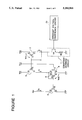
- FIG. 1 is a circuit diagram of a first embodiment of the current mirror type constant current source circuit in accordance with the present invention
- FIG. 2 is a graph illustrating a voltage supply voltage dependence of a current of an input-path n-channel transistor incorporated in the current mirror type constant current source circuit shown in FIG. 1;
- FIG. 3 is a graph illustrating a voltage supply voltage dependence of a current of an output-path n-channel transistor incorporated in the current mirror type constant current source circuit shown in FIG. 1;
- FIGS. 4, 5 and 6 are circuit diagrams of second, third and fourth embodiments of the current mirror type constant current source circuit in accordance with the present invention.
- FIG. 1 there is shown a circuit diagram of a first embodiment of the current mirror type constant current source circuit in accordance with the present invention.
- the shown current mirror type constant current source circuit includes a bandgap voltage reference circuit 20, which is composed of NPN bipolar transistors (not shown) and operates to supply a reference voltage to a base of an NPN bipolar transistor 1A having an emitter connected through a resistor 1B to ground.
- the bipolar transistor 1A and the resistor 1B form a constant current circuit 1.
- a collector of the transistor 1A, forming an output of the constant current circuit 1, is connected in common to a gate and a drain of a p-channel MOS transistor 2, and a gate of another p-channel MOS transistor 3.
- a source of each of the p-channel MOS transistors 2 and 3 is connected to a voltage supply voltage V DD .
- the p-channel MOS transistors 2 and 3 form a first current mirror circuit.
- a drain of the p-channel MOS transistor 3 is connected in common to a gate and a drain of an n-channel MOS transistor 4, and a gate of another n-channel MOS transistor 5.
- a source of each of the n-channel MOS transistors 4 and 5 is connected to ground.
- a source-drain path of the n-channel MOS transistor 5 forms a constant current source, and a drain of the n-channel MOS transistor 5 is connected to a load (not shown).
- n-channel MOS transistor 6 is connected in parallel to the n-channel MOS transistor 4, in such a manner that a drain and a source of the n-channel MOS transistor 6 are connected to the drain and the source of the n-channel MOS transistor 4, respectively.
- a gate of the n-channel MOS transistor 6 is connected to the voltage supply voltage V DD .
- the constant current circuit 1 and hence the bipolar transistor 1A will generate a collector current I 1 , which also flows through the p-channel MOS transistor 2.
- a gate-source voltage V GS1 appears between the gate and the source of the p-channel MOS transistor 2.
- the gate-source voltage V GS1 is determined by the current I 1 in accordance with the characteristics of the p-channel MOS transistor 2.
- the same gate-source voltage V GS1 is applied between the gate and the source of the p-channel MOS transistor 3. Therefore, the p-channel MOS transistor 3 permits to flow a current I 3 therethrough, which is determined by the gate-source voltage in accordance with the characteristics of the p-channel MOS transistor 3.
- This current I 3 flows through the n-channel MOS transistors 4 and 6. Therefore, a gate-source voltage V GS4 appears between the gate and the source of the n-channel MOS transistor 4, which gate-source voltage V GS4 is determined by the current I 3 in accordance with the characteristics of the n-channel MOS transistor 4.
- This gate-source voltage V GS4 is applied between the gate and the source of the n-channel MOS transistor 5. Therefore, the n-channel MOS transistor 5 permits to flow a current I 5 therethrough, which is determined by the gate-source voltage in accordance with the characteristics of the n-channel MOS transistor 5.
- This current I 5 is used as a constant current which will be flowed through another circuit (not shown).
- a solid line shows a voltage supply voltage dependence of a source-drain current of the n-channel MOS transistor 4 having the parallel-connected MOS transistor 6
- a dotted line shows a voltage supply voltage dependence of a source-drain current of the n-channel MOS transistor 4 in the case of having no parallel-connected MOS transistor 6.
- the n-channel MOS transistor 4 having the parallel-connected MOS transistor 6 has a decreased dependence upon the voltage supply voltage.
- the reason for this is that: When the voltage supply voltage increases, the current I 3 of the p-channel MOS transistor 3 also increases, but at this time, since the gate bias of the n-channel MOS transistor 6 is increased by the increased voltage supply voltage, the amount increased of the current I 3 of the p-channel MOS transistor 3 is flowed or absorbed by the n-channel MOS transistor 6. Therefore, a change of the gate-source voltage V GS4 caused by the increase of the voltage supply voltage is limited to a minimum extent.
- the n-channel MOS transistor 5 has a current-voltage supply voltage characteristics as shown by a solid line in FIG. 3.
- a dotted line shows a voltage supply voltage dependence of a source-drain current of the n-channel MOS transistor 5 in the case of having no n-channel MOS transistor 6.
- the voltage supply voltage dependence of the output current is improved in the embodiment shown in FIG. 1. Therefore, the embodiment shown in FIG. 1 can remarkably restrain or minimize the voltage supply voltage dependence of a constant current source in a semiconductor integrated circuit.
- FIG. 4 there is shown a second embodiment of the current mirror type constant current source circuit in accordance with the present invention.
- elements similar to those shown in FIG. 1 are given the same reference numerals, and explanation thereof will be omitted for simplification of description.
- the second embodiment is characterized by addition of a p-channel MOS transistor 7 which has a drain connected to the drain of the p-channel MOS transistor 2, and a source connected to the high voltage V DD .
- a gate of the p-channel MOS transistor 7 is connected to the ground.
- FIG. 5 there is shown a third embodiment of the current mirror type constant current source circuit in accordance with the present invention.
- elements similar to those shown in FIG. 4 are given the same reference numerals, and explanation thereof will be omitted for simplification of description.
- the third embodiment is characterized by addition of a pair of parallel connected p-channel MOS transistors 8 and 9, each of which has a drain connected to the drain of the n-channel transistor 5, and a source connected to the voltage supply voltage V DD .
- a gate of the p-channel MOS transistor 8 is grounded, and a gate of the p-channel MOS transistor 9 is connected to the drain of the p-channel MOS transistor 9 itself, and also connected an output voltage terminal 10.
- a current-voltage supply voltage characteristics of the p-channel MOS transistor 9 is adjusted by the p-channel MOS transistor 8, so that a high level reference voltage having less dependence upon the voltage supply voltage can be obtained from the output terminal 10 connected to the gate of the p-channel MOS transistor 9.
- FIG. 6 there is shown a fourth embodiment of the current mirror type constant current source circuit in accordance with the present invention.
- the shown fourth embodiment of the current mirror type constant current source circuit includes a bandgap voltage reference circuit 30 which includes of PNP bipolar transistors (not shown) and which supplies a reference voltage to a base of a PNP bipolar transistor 32A, which has an emitter connected through a resistor 32B to a high voltage V DD .
- the bipolar transistor 32A and the resistor 32B form a constant current circuit 32.
- a collector of the transistor 32A, forming an output of the constant current circuit 32, is connected in common to a gate and a drain of an n-channel MOS transistor 34, and a gate of another p-channel MOS transistor 36.
- a source of each of the n-channel MOS transistors 34 and 36 is connected to the ground.
- the n-channel MOS transistors 34 and 36 form a current mirror circuit.
- n-channel MOS transistor 38 is connected in parallel to the n-channel MOS transistor 34, in such a manner that a drain and a source of the n-channel MOS transistor 38 are connected to the drain and the source of the n-channel MOS transistor 34, respectively.
- a gate of the n-channel MOS transistor 38 is connected to the voltage supply voltage V DD .
- the constant current circuit 32 and hence the bipolar transistor 32A will generate a collector current I 32 , which flows through the n-channel MOS transistors 34 and 38.
- a gate-source voltage V GS34 appears between the gate and the source of the n-channel MOS transistor 34.
- the gate-source voltage V GS34 is determined by the current I 32 in accordance with the characteristics of the n-channel MOS transistor 34.
- the same gate-source voltage V GS34 is applied between the gate and the source of the n-channel MOS transistor 36. Therefore, the n-channel MOS transistor 36 permits to flow a current I 36 therethrough, which is determined by the gate-source voltage in accordance with the characteristics of the n-channel MOS transistor 36.
- the current I 32 flowing through the PNP transistor 32A is partially shunted or bypassed to the n-channel MOS transistor 38.
- This n-channel MOS transistor 38 operates similarly to the n-channel MOS transistor 6 of the first embodiment when the voltage supply voltage increases. Therefore, the voltage supply voltage dependence of the current of the n-channel MOS transistor 36 can be restrained or minimized.
- the present invention is characterized by connecting in parallel to a current path MOS transistor, an additional MOS transistor of the same channel type having a gate connected to a voltage supply voltage.
- the current-voltage supply voltage characteristics of the current path MOS transistor is modified so that the amount increased of the current of the current path MOS transistor when a voltage supply voltage increases can be remarkably reduced in comparison with the case in which no addition MOS transistor is connected in parallel to the current path MOS transistor. If the current path MOS transistor having the parallel-connected additional MOS transistor connected is used as an input current path MOS transistor of a current mirror type constant current source circuit, the constant current source circuit having less dependence upon the voltage supply voltage can be obtained.
Landscapes
- Engineering & Computer Science (AREA)
- Physics & Mathematics (AREA)
- Microelectronics & Electronic Packaging (AREA)
- Nonlinear Science (AREA)
- Electromagnetism (AREA)
- General Physics & Mathematics (AREA)
- Radar, Positioning & Navigation (AREA)
- Automation & Control Theory (AREA)
- Control Of Electrical Variables (AREA)
- Amplifiers (AREA)
Applications Claiming Priority (2)
| Application Number | Priority Date | Filing Date | Title |
|---|---|---|---|
| JP2220204A JP2715642B2 (ja) | 1990-08-22 | 1990-08-22 | 半導体集積回路 |
| JP2-220204 | 1990-08-22 |
Publications (1)
| Publication Number | Publication Date |
|---|---|
| US5180966A true US5180966A (en) | 1993-01-19 |
Family
ID=16747521
Family Applications (1)
| Application Number | Title | Priority Date | Filing Date |
|---|---|---|---|
| US07/748,994 Expired - Fee Related US5180966A (en) | 1990-08-22 | 1991-08-22 | Current mirror type constant current source circuit having less dependence upon supplied voltage |
Country Status (4)
| Country | Link |
|---|---|
| US (1) | US5180966A (fr) |
| EP (1) | EP0472202B1 (fr) |
| JP (1) | JP2715642B2 (fr) |
| DE (1) | DE69114079T2 (fr) |
Cited By (14)
| Publication number | Priority date | Publication date | Assignee | Title |
|---|---|---|---|---|
| US5304861A (en) * | 1989-09-12 | 1994-04-19 | Sgs-Thomson Microelectronics S.A. | Circuit for the detection of temperature threshold, light and unduly low clock frequency |
| US5357188A (en) * | 1991-07-25 | 1994-10-18 | Rohm Co., Ltd. | Current mirror circuit operable with a low power supply voltage |
| US5453953A (en) * | 1991-10-03 | 1995-09-26 | International Business Machines Corporation | Bandgap voltage reference generator |
| US5629609A (en) * | 1994-03-08 | 1997-05-13 | Texas Instruments Incorporated | Method and apparatus for improving the drop-out voltage in a low drop out voltage regulator |
| US5661395A (en) * | 1995-09-28 | 1997-08-26 | International Business Machines Corporation | Active, low Vsd, field effect transistor current source |
| US5663674A (en) * | 1994-05-11 | 1997-09-02 | Siemens Aktiengesellschaft | Circut configuration for generating a reference current |
| US5694032A (en) * | 1996-03-19 | 1997-12-02 | International Business Machines Corporation | Band gap current reference circuit |
| US5696440A (en) * | 1993-09-30 | 1997-12-09 | Nec Corporation | Constant current generating apparatus capable of stable operation |
| US5864230A (en) * | 1997-06-30 | 1999-01-26 | Lsi Logic Corporation | Variation-compensated bias current generator |
| US6160393A (en) * | 1999-01-29 | 2000-12-12 | Samsung Electronics Co., Ltd. | Low power voltage reference circuit |
| US6342781B1 (en) * | 2001-04-13 | 2002-01-29 | Ami Semiconductor, Inc. | Circuits and methods for providing a bandgap voltage reference using composite resistors |
| US6566851B1 (en) | 2000-08-10 | 2003-05-20 | Applied Micro Circuits, Corporation | Output conductance correction circuit for high compliance short-channel MOS switched current mirror |
| US7230467B1 (en) * | 2005-03-24 | 2007-06-12 | Cirrus Logic, Inc. | Constant edge generation circuits and methods and systems using the same |
| US20130057335A1 (en) * | 2011-09-06 | 2013-03-07 | Nobuhiro Kawai | Power supply stabilizing circuit of solid-state imaging device |
Families Citing this family (3)
| Publication number | Priority date | Publication date | Assignee | Title |
|---|---|---|---|---|
| GB9417267D0 (en) * | 1994-08-26 | 1994-10-19 | Inmos Ltd | Current generator circuit |
| EP0731403A3 (fr) * | 1995-03-08 | 1997-07-23 | Sgs Thomson Microelectronics | Source de courant constante |
| FR2821443B1 (fr) * | 2001-02-26 | 2003-06-20 | St Microelectronics Sa | Source de courant apte a fonctionner sous faible tension d'alimentation et a variation de courant avec la tension d'alimentation quasi nulle |
Citations (6)
| Publication number | Priority date | Publication date | Assignee | Title |
|---|---|---|---|---|
| US4327321A (en) * | 1979-06-19 | 1982-04-27 | Tokyo Shibaura Denki Kabushiki Kaisha | Constant current circuit |
| US4499416A (en) * | 1981-11-25 | 1985-02-12 | Tokyo Shibaura Denki Kabushiki Kaisha | Reference voltage circuit for obtaining a constant voltage irrespective of the fluctuations of a power supply voltage |
| US4536702A (en) * | 1982-04-05 | 1985-08-20 | Tokyo Shibaura Denki Kabushiki Kaisha | Constant current source or voltage source transistor circuit |
| US4727309A (en) * | 1987-01-22 | 1988-02-23 | Intel Corporation | Current difference current source |
| EP0310743A2 (fr) * | 1987-10-08 | 1989-04-12 | International Business Machines Corporation | Source de courant contrôlée |
| US4943737A (en) * | 1989-10-13 | 1990-07-24 | Advanced Micro Devices, Inc. | BICMOS regulator which controls MOS transistor current |
Family Cites Families (3)
| Publication number | Priority date | Publication date | Assignee | Title |
|---|---|---|---|---|
| DE3138558A1 (de) * | 1981-09-28 | 1983-04-07 | Siemens AG, 1000 Berlin und 8000 München | Schaltungsanordnung zur erzeugung eines von schwankungen einer versorgungsgleichspannung freien gleichspannungspegels |
| JPH0416493Y2 (fr) * | 1986-07-28 | 1992-04-14 | ||
| US4742292A (en) * | 1987-03-06 | 1988-05-03 | International Business Machines Corp. | CMOS Precision voltage reference generator |
-
1990
- 1990-08-22 JP JP2220204A patent/JP2715642B2/ja not_active Expired - Lifetime
-
1991
- 1991-08-22 EP EP91114103A patent/EP0472202B1/fr not_active Expired - Lifetime
- 1991-08-22 DE DE69114079T patent/DE69114079T2/de not_active Expired - Fee Related
- 1991-08-22 US US07/748,994 patent/US5180966A/en not_active Expired - Fee Related
Patent Citations (6)
| Publication number | Priority date | Publication date | Assignee | Title |
|---|---|---|---|---|
| US4327321A (en) * | 1979-06-19 | 1982-04-27 | Tokyo Shibaura Denki Kabushiki Kaisha | Constant current circuit |
| US4499416A (en) * | 1981-11-25 | 1985-02-12 | Tokyo Shibaura Denki Kabushiki Kaisha | Reference voltage circuit for obtaining a constant voltage irrespective of the fluctuations of a power supply voltage |
| US4536702A (en) * | 1982-04-05 | 1985-08-20 | Tokyo Shibaura Denki Kabushiki Kaisha | Constant current source or voltage source transistor circuit |
| US4727309A (en) * | 1987-01-22 | 1988-02-23 | Intel Corporation | Current difference current source |
| EP0310743A2 (fr) * | 1987-10-08 | 1989-04-12 | International Business Machines Corporation | Source de courant contrôlée |
| US4943737A (en) * | 1989-10-13 | 1990-07-24 | Advanced Micro Devices, Inc. | BICMOS regulator which controls MOS transistor current |
Cited By (16)
| Publication number | Priority date | Publication date | Assignee | Title |
|---|---|---|---|---|
| US5304861A (en) * | 1989-09-12 | 1994-04-19 | Sgs-Thomson Microelectronics S.A. | Circuit for the detection of temperature threshold, light and unduly low clock frequency |
| US5357188A (en) * | 1991-07-25 | 1994-10-18 | Rohm Co., Ltd. | Current mirror circuit operable with a low power supply voltage |
| US5453953A (en) * | 1991-10-03 | 1995-09-26 | International Business Machines Corporation | Bandgap voltage reference generator |
| US5696440A (en) * | 1993-09-30 | 1997-12-09 | Nec Corporation | Constant current generating apparatus capable of stable operation |
| US5629609A (en) * | 1994-03-08 | 1997-05-13 | Texas Instruments Incorporated | Method and apparatus for improving the drop-out voltage in a low drop out voltage regulator |
| US5663674A (en) * | 1994-05-11 | 1997-09-02 | Siemens Aktiengesellschaft | Circut configuration for generating a reference current |
| US5661395A (en) * | 1995-09-28 | 1997-08-26 | International Business Machines Corporation | Active, low Vsd, field effect transistor current source |
| US5694032A (en) * | 1996-03-19 | 1997-12-02 | International Business Machines Corporation | Band gap current reference circuit |
| US5864230A (en) * | 1997-06-30 | 1999-01-26 | Lsi Logic Corporation | Variation-compensated bias current generator |
| US6072306A (en) * | 1997-06-30 | 2000-06-06 | Lsi Logic Corporation | Variation-compensated bias current generator |
| US6160393A (en) * | 1999-01-29 | 2000-12-12 | Samsung Electronics Co., Ltd. | Low power voltage reference circuit |
| US6566851B1 (en) | 2000-08-10 | 2003-05-20 | Applied Micro Circuits, Corporation | Output conductance correction circuit for high compliance short-channel MOS switched current mirror |
| US6342781B1 (en) * | 2001-04-13 | 2002-01-29 | Ami Semiconductor, Inc. | Circuits and methods for providing a bandgap voltage reference using composite resistors |
| US7230467B1 (en) * | 2005-03-24 | 2007-06-12 | Cirrus Logic, Inc. | Constant edge generation circuits and methods and systems using the same |
| US20130057335A1 (en) * | 2011-09-06 | 2013-03-07 | Nobuhiro Kawai | Power supply stabilizing circuit of solid-state imaging device |
| CN102981539A (zh) * | 2011-09-06 | 2013-03-20 | 株式会社东芝 | 电源稳定化电路 |
Also Published As
| Publication number | Publication date |
|---|---|
| DE69114079D1 (de) | 1995-11-30 |
| EP0472202A3 (en) | 1992-09-02 |
| DE69114079T2 (de) | 1996-05-23 |
| JP2715642B2 (ja) | 1998-02-18 |
| JPH04102107A (ja) | 1992-04-03 |
| EP0472202B1 (fr) | 1995-10-25 |
| EP0472202A2 (fr) | 1992-02-26 |
Similar Documents
| Publication | Publication Date | Title |
|---|---|---|
| US5180966A (en) | Current mirror type constant current source circuit having less dependence upon supplied voltage | |
| US5311115A (en) | Enhancement-depletion mode cascode current mirror | |
| US5059890A (en) | Constant current source circuit | |
| US6407537B2 (en) | Voltage regulator provided with a current limiter | |
| US4008441A (en) | Current amplifier | |
| US6034519A (en) | Internal supply voltage generating circuit | |
| US6169456B1 (en) | Auto-biasing circuit for current mirrors | |
| US4461991A (en) | Current source circuit having reduced error | |
| US5635869A (en) | Current reference circuit | |
| US5801523A (en) | Circuit and method of providing a constant current | |
| US5166553A (en) | Current mirror circuit employing depletion mode FETs | |
| JPH0679262B2 (ja) | 参照電圧回路 | |
| US4336503A (en) | Driver circuit having reduced cross-over distortion | |
| US5883507A (en) | Low power temperature compensated, current source and associated method | |
| US4602207A (en) | Temperature and power supply stable current source | |
| US20070194838A1 (en) | Current mirror with improved output impedance at low power supplies | |
| US6809575B2 (en) | Temperature-compensated current reference circuit | |
| JP4176152B2 (ja) | 分圧器回路 | |
| US5966006A (en) | Voltage regulator generating a predetermined temperature-stable voltage | |
| US5132566A (en) | BiMOS semiconductor integrated circuit having short-circuit protection | |
| US6072306A (en) | Variation-compensated bias current generator | |
| US6100753A (en) | Bias stabilization circuit | |
| US5349307A (en) | Constant current generation circuit of current mirror type having equal input and output currents | |
| US6639453B2 (en) | Active bias circuit having wilson and widlar configurations | |
| KR100332508B1 (ko) | 안정화전류미러회로 |
Legal Events
| Date | Code | Title | Description |
|---|---|---|---|
| AS | Assignment |
Owner name: NEC CORPORATION, JAPAN Free format text: ASSIGNMENT OF ASSIGNORS INTEREST.;ASSIGNORS:SUGAWARA, MICHINORI;TAKAHASHI, HIROYUKI;REEL/FRAME:005928/0980 Effective date: 19911016 |
|
| FEPP | Fee payment procedure |
Free format text: PAYOR NUMBER ASSIGNED (ORIGINAL EVENT CODE: ASPN); ENTITY STATUS OF PATENT OWNER: LARGE ENTITY |
|
| FPAY | Fee payment |
Year of fee payment: 4 |
|
| FEPP | Fee payment procedure |
Free format text: PAYOR NUMBER ASSIGNED (ORIGINAL EVENT CODE: ASPN); ENTITY STATUS OF PATENT OWNER: LARGE ENTITY Free format text: PAYER NUMBER DE-ASSIGNED (ORIGINAL EVENT CODE: RMPN); ENTITY STATUS OF PATENT OWNER: LARGE ENTITY |
|
| FPAY | Fee payment |
Year of fee payment: 8 |
|
| REMI | Maintenance fee reminder mailed | ||
| LAPS | Lapse for failure to pay maintenance fees | ||
| STCH | Information on status: patent discontinuation |
Free format text: PATENT EXPIRED DUE TO NONPAYMENT OF MAINTENANCE FEES UNDER 37 CFR 1.362 |
|
| FP | Lapsed due to failure to pay maintenance fee |
Effective date: 20050119 |