US5257155A - Short-circuit proof field effect transistor - Google Patents
Short-circuit proof field effect transistor Download PDFInfo
- Publication number
- US5257155A US5257155A US07/749,020 US74902091A US5257155A US 5257155 A US5257155 A US 5257155A US 74902091 A US74902091 A US 74902091A US 5257155 A US5257155 A US 5257155A
- Authority
- US
- United States
- Prior art keywords
- coupled
- field effect
- effect transistor
- resistor
- terminal
- Prior art date
- Legal status (The legal status is an assumption and is not a legal conclusion. Google has not performed a legal analysis and makes no representation as to the accuracy of the status listed.)
- Expired - Lifetime
Links
- 230000005669 field effect Effects 0.000 title claims abstract description 62
- 239000003990 capacitor Substances 0.000 claims description 7
- 230000006378 damage Effects 0.000 abstract description 6
- 238000010586 diagram Methods 0.000 description 4
- 230000004075 alteration Effects 0.000 description 2
- 238000012986 modification Methods 0.000 description 2
- 230000004048 modification Effects 0.000 description 2
- 238000012544 monitoring process Methods 0.000 description 2
- 230000003247 decreasing effect Effects 0.000 description 1
- 230000003111 delayed effect Effects 0.000 description 1
- 230000001939 inductive effect Effects 0.000 description 1
- 230000000630 rising effect Effects 0.000 description 1
Images
Classifications
-
- H—ELECTRICITY
- H03—ELECTRONIC CIRCUITRY
- H03K—PULSE TECHNIQUE
- H03K17/00—Electronic switching or gating, i.e. not by contact-making and –breaking
- H03K17/08—Modifications for protecting switching circuit against overcurrent or overvoltage
- H03K17/082—Modifications for protecting switching circuit against overcurrent or overvoltage by feedback from the output to the control circuit
- H03K17/0822—Modifications for protecting switching circuit against overcurrent or overvoltage by feedback from the output to the control circuit in field-effect transistor switches
Definitions
- This invention relates to circuits, for example, a circuit to provide short-circuit protection for a field effect transistor.
- At least one attempt to provide short-circuit protection for a power device includes sensing the current through the power device by monitoring the voltage across a sense resistor which is coupled in series with the power device. When the current through the power device reaches a predetermined level, the voltage across the sense resistor turns on a bipolar transistor thereby reducing the drive to the power device.
- this attempt dissipates a large amount of power and possesses a high on-resistance.
- Another attempt at providing short-circuit protection for a power device includes monitoring the temperature of the die of which the power device is fabricated on. In this attempt, the power device is turned off when the temperature of the die exceeds a predetermined limit. However, if destruction to the power device occurs before the temperature exceeds the predetermined limit, this attempt becomes futile.
- a protection circuit for a field effect transistor the field effect transistor having gate, source and drain electrodes
- the protection circuit comprising a sensing circuit having an input and an output, the input of the sensing circuit being coupled to the drain electrode of the field effect transistor for detecting when the voltage appearing at the drain electrode of the field effect transistor exceeds a predetermined voltage; a delay circuit having an input and an output, the input of the delay circuit being coupled to receive a control signal; a gate circuit having first and second inputs and an output, the first and second inputs of the gate circuit being respectively coupled to the outputs of the delay circuit and the sensing circuit, the output of the gate circuit providing a logic signal to the gate electrode of the field effect transistor; and a first resistor coupled between the input of the delay circuit and the gate electrode of the field effect transistor.
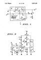
- FIG. 1 is a partial schematic/block diagram illustrating a short-circuit proof field effect transistor in accordance with the present invention.
- FIG. 2 is a detailed schematic diagram illustrating a short-circuit proof field effect transistor in accordance with the present invention.
- FIG. 1 a partial schematic/block diagram illustrating short-circuit proof field effect transistor circuit 10 is shown comprising field effect transistor (FET) 12 having its drain, source and gate electrodes respectively coupled to terminals 14, 16 and 18.
- FET field effect transistor
- Protection circuit 20 has a first input coupled to terminal 14 and a second input coupled to terminal 22 at which a drive signal for FET 12 is provided. The output of protection circuit 20 is coupled to terminal 18.
- short-circuit proof field effect transistor circuit 10 has a control input coupled to terminal 22, and current carrying electrodes coupled to terminals 14 and 16.
- Protection circuit 20 includes delay circuit 26 having an input coupled to terminal 22 and an output coupled to a first input of NAND gate 28.
- the second input of NAND gate 28 is coupled to circuit node 30 whereby circuit node 30 is returned to ground through resistor 32.
- circuit node 30 is coupled to terminal 14 via resistor 34.
- Resistors 32 and 34 form sense circuit 36 which is used to sense the voltage appearing at terminal 14. That is, as the voltage at terminal 14 increases, the voltage at circuit node 30 also increases.
- NAND gate 28 The output of NAND gate 28 is coupled to terminal 18. Further, resistor 38 is coupled between terminals 22 and 18.
- protection circuit 20 detects when a short-circuit condition through a load (not shown) which is coupled in series with terminal 14 occurs. In response to the short-circuit condition, protection circuit 20 functions to turns off the gate drive to FET 12 thereby preventing damage to FET 12.
- the voltage appearing at the drain electrode of FET 12 is sensed via sense circuit 36. That is, when the voltage appearing at the drain electrode of FET 12 reaches a first predetermined voltage, the voltage appearing at circuit node 30 reaches a second predetermined voltage. This second predetermined voltage is indicative of a logic high voltage level and is applied to the second input of NAND gate 28.
- the signal applied to terminal 22 is delayed by a predetermined time via delay circuit 26, and is then applied to the first input of NAND gate 28. If both signals appearing at first and second inputs of NAND gate 28 are at a logic high voltage level, NAND gate 28 responds to provide a logic low voltage level to the gate electrode of FET 12 thereby turning off FET 12 thereby preventing damage to FET 12.
- delay circuit 26 allows the voltage appearing at the drain electrode of FET 26 to fall to a logic low voltage level during normal operation, as aforedescribed. Thus, when a logic high voltage level is applied to terminal 22, protection circuit 20 will not turn off FET 12 if the voltage at the drain electrode of FET 12 reaches a logic low voltage level within a predetermined time.
- FIG. 2 a detailed schematic diagram illustrating short-circuit proof field effect transistor circuit 10 is shown. It is understood that components shown in FIG. 2 which are identical to components shown in FIG. 1 are identified by like reference numbers.
- NAND gate 28 is formed by field effect transistors (FET's) 40 and 44 wherein FET 40 has a drain electrode coupled to circuit node 42 and a gate electrode coupled to circuit node 30.
- FET 40 has a drain electrode coupled to circuit node 42 and a gate electrode coupled to circuit node 30.
- the source electrode of FET 40 is coupled to the drain electrode of FET 44, the latter having a source electrode coupled returned to ground.
- Delay circuit 26 is formed by resistor 46 and capacitor 48.
- the first terminal of resistor 46 is coupled to terminal 22, while the second terminal of resistor 46 is coupled to the gate electrode of FET 44 and to the first terminal of capacitor 48.
- the second terminal of capacitor 48 is returned to ground.
- Resistor 50 is coupled between the second terminal of resistor 46 and ground potential. In particular, for the case of slowly rising signals at terminal 22, resistor 50 ensures that FET 12 turns on before FET 44 turns on.
- the circuit of FIG. 2 further includes resistor 52 coupled between terminal 22 and circuit node 42, and resistor 54 coupled between terminal 18 and circuit node 42.
- Terminal 14 is coupled to circuit node 56 via resistor 58 wherein circuit node 56 is coupled to circuit node 30 via resistor 34. Circuit node 56 is also coupled through load resistor 60 to a first supply voltage terminal.
- Back-to-back diodes 62 and 64 have respective cathodes which are coupled to terminals 56 and 18.
- the anode of diode 62 is coupled to the anode of diode 64.
- back-to-back diodes 66 and 68 have respective cathodes which are coupled to circuit node 30 and ground potential.
- the anode of diode 66 is coupled to the anode of diode 68.
- Diodes 66 and 68 function to limit the maximum voltage appearing at the gate electrode of FET 40 to a predetermined value thereby preventing destruction to NAND gate 28.
- the operation of the circuit shown in FIG. 2 is identical to the aforedescribed operation for the circuit shown in FIG. 1. Briefly, when the gate electrodes of 40 and 44 are at a logic high voltage level, the gate electrode of FET 12 is pulled to a logic low voltage level wherein the voltage across resistor 52 increases thereby decreasing the voltage at the gate of FET 12.
- the protection circuit senses when the voltage appearing at the gate and drain electrodes of the field effect transistor are both at a logic high voltage level, and responds to turn off the field effect transistor.
Landscapes
- Protection Of Static Devices (AREA)
- Amplifiers (AREA)
- Semiconductor Integrated Circuits (AREA)
Priority Applications (3)
| Application Number | Priority Date | Filing Date | Title |
|---|---|---|---|
| US07/749,020 US5257155A (en) | 1991-08-23 | 1991-08-23 | Short-circuit proof field effect transistor |
| JP4236507A JPH05206748A (ja) | 1991-08-23 | 1992-08-12 | 電界効果トランジスタのための保護回路 |
| EP19920113954 EP0529448A3 (en) | 1991-08-23 | 1992-08-17 | Field effect transistor protection circuit |
Applications Claiming Priority (1)
| Application Number | Priority Date | Filing Date | Title |
|---|---|---|---|
| US07/749,020 US5257155A (en) | 1991-08-23 | 1991-08-23 | Short-circuit proof field effect transistor |
Publications (1)
| Publication Number | Publication Date |
|---|---|
| US5257155A true US5257155A (en) | 1993-10-26 |
Family
ID=25011887
Family Applications (1)
| Application Number | Title | Priority Date | Filing Date |
|---|---|---|---|
| US07/749,020 Expired - Lifetime US5257155A (en) | 1991-08-23 | 1991-08-23 | Short-circuit proof field effect transistor |
Country Status (3)
| Country | Link |
|---|---|
| US (1) | US5257155A (fr) |
| EP (1) | EP0529448A3 (fr) |
| JP (1) | JPH05206748A (fr) |
Cited By (5)
| Publication number | Priority date | Publication date | Assignee | Title |
|---|---|---|---|---|
| US5684663A (en) * | 1995-09-29 | 1997-11-04 | Motorola, Inc. | Protection element and method for protecting a circuit |
| US5737169A (en) * | 1996-02-28 | 1998-04-07 | Eni, A Division Of Astec America, Inc. | Intrinsic element sensing integrated SOA protection for power MOSFET switches |
| WO1998059421A1 (fr) * | 1997-06-10 | 1998-12-30 | A. Ahlstrom Corporation | Protection contre les court-circuits d'un interrupteur a semi-conducteur |
| US6460626B2 (en) | 1998-12-30 | 2002-10-08 | Black & Decker Inc. | Dual-mode non-isolated corded system for transportable cordless power tools |
| DE10137499C1 (de) * | 2001-07-31 | 2003-02-20 | Siemens Ag | Schaltungsanordnung zur Überwachung eines Schaltelements |
Families Citing this family (3)
| Publication number | Priority date | Publication date | Assignee | Title |
|---|---|---|---|---|
| DE19936857A1 (de) * | 1999-08-05 | 2001-02-15 | Siemens Ag | Schutzschaltung für ein elektrisches Schaltelement |
| JP2010118548A (ja) * | 2008-11-13 | 2010-05-27 | Mitsubishi Electric Corp | 半導体装置 |
| DE102011005708A1 (de) * | 2011-03-17 | 2012-09-20 | Sb Limotive Company Ltd. | Vorrichtung zum Abschalten eines Leistungs-Transistors |
Citations (1)
| Publication number | Priority date | Publication date | Assignee | Title |
|---|---|---|---|---|
| US4937697A (en) * | 1989-05-22 | 1990-06-26 | Motorola, Inc. | Semiconductor device protection circuit |
Family Cites Families (5)
| Publication number | Priority date | Publication date | Assignee | Title |
|---|---|---|---|---|
| US4363068A (en) * | 1980-08-18 | 1982-12-07 | Sundstrand Corporation | Power FET short circuit protection |
| DE3366617D1 (en) * | 1982-10-12 | 1986-11-06 | Nissan Motor | A semiconductor switching circuit with an overcurrent protection |
| US4893211A (en) * | 1985-04-01 | 1990-01-09 | Motorola, Inc. | Method and circuit for providing adjustable control of short circuit current through a semiconductor device |
| US4808839A (en) * | 1988-04-04 | 1989-02-28 | Motorola, Inc. | Power field effect transistor driver circuit for protection from overvoltages |
| EP0384937A1 (fr) * | 1989-03-03 | 1990-09-05 | Siemens Aktiengesellschaft | Circuit de protection pour une MOSFET de puissance |
-
1991
- 1991-08-23 US US07/749,020 patent/US5257155A/en not_active Expired - Lifetime
-
1992
- 1992-08-12 JP JP4236507A patent/JPH05206748A/ja active Pending
- 1992-08-17 EP EP19920113954 patent/EP0529448A3/en not_active Ceased
Patent Citations (1)
| Publication number | Priority date | Publication date | Assignee | Title |
|---|---|---|---|---|
| US4937697A (en) * | 1989-05-22 | 1990-06-26 | Motorola, Inc. | Semiconductor device protection circuit |
Cited By (7)
| Publication number | Priority date | Publication date | Assignee | Title |
|---|---|---|---|---|
| US5684663A (en) * | 1995-09-29 | 1997-11-04 | Motorola, Inc. | Protection element and method for protecting a circuit |
| US5737169A (en) * | 1996-02-28 | 1998-04-07 | Eni, A Division Of Astec America, Inc. | Intrinsic element sensing integrated SOA protection for power MOSFET switches |
| WO1998059421A1 (fr) * | 1997-06-10 | 1998-12-30 | A. Ahlstrom Corporation | Protection contre les court-circuits d'un interrupteur a semi-conducteur |
| US6160693A (en) * | 1997-06-10 | 2000-12-12 | Oy Lexel Finland Ab | Short circuit protection for a semiconductor switch |
| US6460626B2 (en) | 1998-12-30 | 2002-10-08 | Black & Decker Inc. | Dual-mode non-isolated corded system for transportable cordless power tools |
| US6675912B2 (en) | 1998-12-30 | 2004-01-13 | Black & Decker Inc. | Dual-mode non-isolated corded system for transportable cordless power tools |
| DE10137499C1 (de) * | 2001-07-31 | 2003-02-20 | Siemens Ag | Schaltungsanordnung zur Überwachung eines Schaltelements |
Also Published As
| Publication number | Publication date |
|---|---|
| EP0529448A2 (fr) | 1993-03-03 |
| EP0529448A3 (en) | 1993-12-08 |
| JPH05206748A (ja) | 1993-08-13 |
Similar Documents
| Publication | Publication Date | Title |
|---|---|---|
| US5914545A (en) | Switching device with power FET and short-circuit detection | |
| EP0369448B1 (fr) | Circuit d'attaque utilisable pour dispositif semi-conducteur commandé en tension | |
| US4679112A (en) | Transistor protection circuit for automotive motor control applications | |
| US5506539A (en) | IGFET power semiconductor circuit with GAE control and fault detection circuits | |
| US4429339A (en) | AC Transistor switch with overcurrent protection | |
| US5724218A (en) | Power transistor with short-circuit protection | |
| US4893211A (en) | Method and circuit for providing adjustable control of short circuit current through a semiconductor device | |
| EP0426103B1 (fr) | Dispositif électronique de protection contre l'interruption indésirable de la connection à la masse pour circuits électroniques | |
| US4954917A (en) | Power transistor drive circuit with improved short circuit protection | |
| US5418673A (en) | Control electrode disable circuit for power transistor | |
| US4914540A (en) | Overvoltage-protective device | |
| US4547686A (en) | Hybrid power semiconductor switch | |
| US5561391A (en) | Clamp circuit and method for detecting an activation of same | |
| US20040264084A1 (en) | Polarity protection implemented with a mosfet | |
| US6008972A (en) | Short circuit protection circuit for a low-side driver circuit | |
| US5257155A (en) | Short-circuit proof field effect transistor | |
| US5360979A (en) | Fast turn-off circuit for solid-state relays or the like | |
| US5432665A (en) | Short circuit protected capacitive load driver | |
| US5424897A (en) | Three leaded protected power device having voltage input | |
| US4979068A (en) | High speed electronic circuit breaker | |
| US3711763A (en) | Overcurrent protection circuit for a voltage regulator | |
| USRE34107E (en) | Power transistor drive circuit with improved short circuit protection | |
| US5625518A (en) | Clamping circuit with reverse polarity protection | |
| US4789842A (en) | Composite transistor device with over-current protection | |
| US5576615A (en) | Method and circuit for detecting faulty recirculation diode in a switched mode power supply |
Legal Events
| Date | Code | Title | Description |
|---|---|---|---|
| AS | Assignment |
Owner name: MOTOROLA, INC., A CORP OF IL, SCHAUMBURG, IL Free format text: ASSIGNMENT OF ASSIGNORS INTEREST.;ASSIGNORS:ROBB, STEPHEN P.;RUTTER, ROBERT E.;REEL/FRAME:005820/0791 Effective date: 19910807 |
|
| STCF | Information on status: patent grant |
Free format text: PATENTED CASE |
|
| FPAY | Fee payment |
Year of fee payment: 4 |
|
| AS | Assignment |
Owner name: CHASE MANHATTAN BANK, THE, AS COLLATERAL AGENT, NE Free format text: SECURITY AGREEMENT;ASSIGNOR:SEMICONDUCTOR COMPONENTS INDUSTRIES, LLC;REEL/FRAME:010281/0057 Effective date: 19990804 |
|
| FEPP | Fee payment procedure |
Free format text: PAYOR NUMBER ASSIGNED (ORIGINAL EVENT CODE: ASPN); ENTITY STATUS OF PATENT OWNER: LARGE ENTITY |
|
| AS | Assignment |
Owner name: SEMICONDUCTOR COMPONENTS INDUSTRIES, LLC, ARIZONA Free format text: ASSIGNMENT OF ASSIGNORS INTEREST;ASSIGNOR:MOTOROLA, INC.;REEL/FRAME:010776/0122 Effective date: 20000414 |
|
| FPAY | Fee payment |
Year of fee payment: 8 |
|
| AS | Assignment |
Owner name: JPMORGAN CHASE BANK, AS COLLATERAL AGENT, NEW YORK Free format text: SUPPLEMENT TO SECURITY AGREEMENT;ASSIGNORS:SEMICONDUCTOR COMPONENTS INDUSTRIES, LLC;SEMICONDUCTOR COMPONENTS OF RHODE ISLAND, INC.;REEL/FRAME:012991/0180 Effective date: 20020505 |
|
| AS | Assignment |
Owner name: WELLS FARGO BANK MINNESOTA, NATIONAL ASSOCIATION, Free format text: SECURITY AGREEMENT;ASSIGNORS:SEMICONDUCTOR COMPONENTS INDUSTRIES, LLC;SEMICONDUCTOR COMPONENTS INDUSTRIES OF RHODE ISLAND, INC.;REEL/FRAME:012958/0638 Effective date: 20020506 |
|
| AS | Assignment |
Owner name: JPMORGAN CHASE BANK, NEW YORK Free format text: SECURITY INTEREST;ASSIGNOR:SEMICONDUCTOR COMPONENTS INDUSTRIES, LLC;REEL/FRAME:014007/0239 Effective date: 20030303 |
|
| FPAY | Fee payment |
Year of fee payment: 12 |
|
| AS | Assignment |
Owner name: SEMICONDUCTOR COMPONENTS INDUSTRIES, LLC, ARIZONA Free format text: RELEASE BY SECURED PARTY;ASSIGNOR:WELLS FARGO BANK MINNESOTA, NATIONAL ASSOCIATION, AS COLLATERAL AGENT;REEL/FRAME:038543/0039 Effective date: 20050217 |