US5296835A - Variable resistor and neuro device using the variable resistor for weighting - Google Patents
Variable resistor and neuro device using the variable resistor for weighting Download PDFInfo
- Publication number
- US5296835A US5296835A US08/083,570 US8357093A US5296835A US 5296835 A US5296835 A US 5296835A US 8357093 A US8357093 A US 8357093A US 5296835 A US5296835 A US 5296835A
- Authority
- US
- United States
- Prior art keywords
- electrodes
- opposed
- chalcogenide semiconductor
- variable resistor
- space
- Prior art date
- Legal status (The legal status is an assumption and is not a legal conclusion. Google has not performed a legal analysis and makes no representation as to the accuracy of the status listed.)
- Expired - Lifetime
Links
Images




Classifications
-
- G—PHYSICS
- G06—COMPUTING OR CALCULATING; COUNTING
- G06N—COMPUTING ARRANGEMENTS BASED ON SPECIFIC COMPUTATIONAL MODELS
- G06N3/00—Computing arrangements based on biological models
- G06N3/02—Neural networks
- G06N3/06—Physical realisation, i.e. hardware implementation of neural networks, neurons or parts of neurons
- G06N3/063—Physical realisation, i.e. hardware implementation of neural networks, neurons or parts of neurons using electronic means
-
- G—PHYSICS
- G11—INFORMATION STORAGE
- G11C—STATIC STORES
- G11C11/00—Digital stores characterised by the use of particular electric or magnetic storage elements; Storage elements therefor
- G11C11/54—Digital stores characterised by the use of particular electric or magnetic storage elements; Storage elements therefor using elements simulating biological cells, e.g. neuron
-
- H—ELECTRICITY
- H01—ELECTRIC ELEMENTS
- H01C—RESISTORS
- H01C7/00—Non-adjustable resistors formed as one or more layers or coatings; Non-adjustable resistors made from powdered conducting material or powdered semi-conducting material with or without insulating material
- H01C7/10—Non-adjustable resistors formed as one or more layers or coatings; Non-adjustable resistors made from powdered conducting material or powdered semi-conducting material with or without insulating material voltage responsive, i.e. varistors
- H01C7/105—Varistor cores
-
- H—ELECTRICITY
- H10—SEMICONDUCTOR DEVICES; ELECTRIC SOLID-STATE DEVICES NOT OTHERWISE PROVIDED FOR
- H10N—ELECTRIC SOLID-STATE DEVICES NOT OTHERWISE PROVIDED FOR
- H10N70/00—Solid-state devices having no potential barriers, and specially adapted for rectifying, amplifying, oscillating or switching
- H10N70/011—Manufacture or treatment of multistable switching devices
- H10N70/061—Shaping switching materials
- H10N70/063—Shaping switching materials by etching of pre-deposited switching material layers, e.g. lithography
-
- H—ELECTRICITY
- H10—SEMICONDUCTOR DEVICES; ELECTRIC SOLID-STATE DEVICES NOT OTHERWISE PROVIDED FOR
- H10N—ELECTRIC SOLID-STATE DEVICES NOT OTHERWISE PROVIDED FOR
- H10N70/00—Solid-state devices having no potential barriers, and specially adapted for rectifying, amplifying, oscillating or switching
- H10N70/20—Multistable switching devices, e.g. memristors
- H10N70/231—Multistable switching devices, e.g. memristors based on solid-state phase change, e.g. between amorphous and crystalline phases, Ovshinsky effect
-
- H—ELECTRICITY
- H10—SEMICONDUCTOR DEVICES; ELECTRIC SOLID-STATE DEVICES NOT OTHERWISE PROVIDED FOR
- H10N—ELECTRIC SOLID-STATE DEVICES NOT OTHERWISE PROVIDED FOR
- H10N70/00—Solid-state devices having no potential barriers, and specially adapted for rectifying, amplifying, oscillating or switching
- H10N70/801—Constructional details of multistable switching devices
- H10N70/821—Device geometry
- H10N70/826—Device geometry adapted for essentially vertical current flow, e.g. sandwich or pillar type devices
-
- H—ELECTRICITY
- H10—SEMICONDUCTOR DEVICES; ELECTRIC SOLID-STATE DEVICES NOT OTHERWISE PROVIDED FOR
- H10N—ELECTRIC SOLID-STATE DEVICES NOT OTHERWISE PROVIDED FOR
- H10N70/00—Solid-state devices having no potential barriers, and specially adapted for rectifying, amplifying, oscillating or switching
- H10N70/801—Constructional details of multistable switching devices
- H10N70/841—Electrodes
-
- H—ELECTRICITY
- H10—SEMICONDUCTOR DEVICES; ELECTRIC SOLID-STATE DEVICES NOT OTHERWISE PROVIDED FOR
- H10N—ELECTRIC SOLID-STATE DEVICES NOT OTHERWISE PROVIDED FOR
- H10N70/00—Solid-state devices having no potential barriers, and specially adapted for rectifying, amplifying, oscillating or switching
- H10N70/801—Constructional details of multistable switching devices
- H10N70/881—Switching materials
- H10N70/882—Compounds of sulfur, selenium or tellurium, e.g. chalcogenides
- H10N70/8822—Sulfides, e.g. CuS
-
- H—ELECTRICITY
- H10—SEMICONDUCTOR DEVICES; ELECTRIC SOLID-STATE DEVICES NOT OTHERWISE PROVIDED FOR
- H10N—ELECTRIC SOLID-STATE DEVICES NOT OTHERWISE PROVIDED FOR
- H10N70/00—Solid-state devices having no potential barriers, and specially adapted for rectifying, amplifying, oscillating or switching
- H10N70/801—Constructional details of multistable switching devices
- H10N70/881—Switching materials
- H10N70/882—Compounds of sulfur, selenium or tellurium, e.g. chalcogenides
- H10N70/8828—Tellurides, e.g. GeSbTe
Definitions
- the present invention relates generally to a Neuro device, and more particularly, to an improvement of a variable resistor playing a weighting role in a Neuro device.
- a Neuro device is a representation of a nerve cell constituting human brains, eyes and the like, that is, a neuron by an electronic circuit.
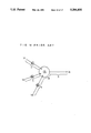
- FIG. 18 is a diagram schematically showing the construction of a neuron.
- a neuron comprises a plurality of synapses and dendrites 1, one nerve cell 2, and one axon.
- the synapse and dendrite 1 corresponds to an input-output interface and an input line in an electronic circuit.
- the nerve cell 2 corresponds to an operational amplifier in the electronic circuit.
- the axon 3 corresponds to an output line in the electronic circuit.
- This neuron acts as follows. Signals V1, V2 and V3 are respectively applied to the three synapses and dendrites 1. Consequently, in the synapses and dendrites 1, weights W1, W2 and W3 are respectively added to the signals V1, V2 and V3.
- the signals entering the nerve cell 2 are weighted, to be V1.W1, V2.W2 and V3.W3.
- the Neuro device is a representation of this neuron by the electronic circuit.
- the synapse, the nerve cell, and the axon and the dendrite constituting the neuron are generally formed of a resistor, an arithmetic circuit, and wires, respectively.
- FIGS. 19, 20 and 21 show examples of circuits of conventional Neuro devices.
- the circuit shown in FIG. 19 comprises n (n : a natural number) input terminals 4, resistors R1, R2, ..., Rn respectively connected to the input terminals 4, an arithmetic circuit 100 to which signals from the resistors R1, R2, ..., Rn are together applied, and an output terminal 5 to which a signal from the arithmetic circuit 100 is outputted.
- n a natural number
- resistors R1, R2, ..., Rn respectively connected to the input terminals 4
- an arithmetic circuit 100 to which signals from the resistors R1, R2, ..., Rn are together applied
- an output terminal 5 to which a signal from the arithmetic circuit 100 is outputted.
- the input currents are added. If the total of the input currents is not less than a predetermined reference current, an output voltage Vx is outputted to the output terminal 5. This voltage Vx is applied to the succeeding Neuro device which is not shown.
- each of the resistors R1 to Rn is a fixed value, so that the weighting cannot be changed. Consequently, a pattern for weighting the input signal is fixed. Therefore, it is proposed that resistors R1, R2, ..., Rn connected to the respective input terminals 4 are made variable, as in an equivalent circuit of FIG. 20.
- FIG. 21 shows an example of a circuit of a Neuro device in which resistors for weighting input signals are variable resistors.
- reference numerals 6 denote weighting portions.
- the weighting portions 6 respectively output voltages corresponding to predetermined weights W1, W2, ..., Wn. Each of the voltages is applied to a gate of a MOSFET (Field Effect Transistor of Metal-Oxide Semiconductor) 7.
- the ON-state resistance value of the MOSFET 7 varies depending on the voltage applied to the gate thereof. Accordingly, a variable resistor for varying the ON-state resistance value of the MOSFET 7 by changing the voltage outputted from the weighting portion 6 is constructed.
- the weighting portion 6 has been conventionally constituted by a cell, a capacitor or a floating gate in a static RAM (see NIKKEI MICRODEVICES, December, 1990, pp. 42 to 51).
- the conventional technique in which the weighting portion 6 is constituted by the cell or the capacitor in the static RAM has the disadvantages in that the area of the variable resistor is large, and data cannot be held in a state where a power supply voltage is off because the cell and the capacitor are volatile.
- the conventional technique in which the weighting portion 6 is constituted by the floating gate has the disadvantage in that it is difficult to implant a desirable amount of charge into the floating gate.
- a first object of the present invention is to overcome the disadvantages of the conventional techniques and to provide a variable resistor having a small occupied area, having a rewritable resistance value and being high in reliability and a Neuro device comprising the variable resistor as a weighting portion.
- a second object of the present invention is to provide a Neuro device using a chalcogenide semiconductor for a weighting circuit.
- a third object of the present invention is to provide an improved variable resistor using a chalcogenide semiconductor which can be utilized for a weighting portion in a Neuro device.
- a weighting portion in a Neuro device is constituted by a variable resistor including a chalcogenide semiconductor.
- the variable resistor comprises a pair of electrodes opposed to each other. The spacing between the pair of opposed electrodes is increased from one end of a space between the pair of opposed electrodes to the other end thereof. The space between the opposed electrodes is filled with the chalcogenide semiconductor.
- variable resistor of the above described construction if a predetermined write voltage is applied to the space between the electrodes, the chalcogenide semiconductor can be transferred from a high resistive state to a low resistive state.
- the write voltage is adjusted, thereby to make it possible to transfer a desirable proportion of the chalcogenide semiconductor into a low resistive state sequentially from the narrowest space between the electrodes to the widest space therebetween.
- the resistance value of the variable resistor can be set to a desirable resistance value.
- variable resistor can be returned to its original state by applying a reset pulse having a voltage value smaller than the write voltage and having a large current value to the space between the electrodes. Consequently, the resistance value of the variable resistor is rewritable.
- FIG. 1 is a diagram showing an electronic circuit of a Neuro device according to one embodiment of the present invention
- FIGS. 2A to 2D are diagrams for explaining the transfer in the state of a chalcogenide semiconductor
- FIG. 3 is diagram for explaining one basic principle of a variable resistor which can be used as a weighting portion in a Neuro device according to the present invention
- FIG. 4 is a diagram for explaining another basic principle of a variable resistor which can be used as a weighting portion in a Neuro device according to the present invention
- FIG. 5 is a diagram specifically showing the construction of a variable resistor which can be used as a weighting portion in a Neuro device according to a first embodiment of the present invention
- FIGS. 6A and 6B are diagrams for explaining a resistance value per unit volume of the variable resistor shown in FIG. 5;
- FIG. 7 is a graph showing the change in the resistance value in a case where the length of a crystallized region of a chalcogenide semiconductor is changed in the variable resistor shown in FIG. 5;
- FIG. 8 is a cross sectional view showing the construction of the variable resistor used in the Neuro device according to the first embodiment of the present invention which is formed on a silicon substrate;
- FIGS. 9A to 9H are cross sectional views showing the manufacturing steps of the variable resistor shown in FIG. 8;
- FIG. 10 is a cross sectional view showing a variable resistor which can be used as a weighting portion in a Neuro device according to a second embodiment of the present invention.
- FIGS. 11A and 11B are diagrams showing a variable resistor which can be used as a weighting portion in a Neuro device according to a third embodiment of the present invention.
- FIG. 12 is an illustration showing the construction of a variable resistor which can be used as a weighting portion in a Neuro device according to a fourth embodiment of the present invention.
- FIG. 13 is a diagram for explaining a resistance value per unit volume of the variable resistor shown in FIG. 12;
- FIG. 14 is a cross sectional view showing the construction of the variable resistor used in the Neuro device according to the fourth embodiment of the present invention which is formed on a silicon substrate;
- FIGS. 15A to 15I are cross sectional views showing the manufacturing steps of the variable resistor shown in FIG. 14;
- FIGS. 16A and 16B are diagrams showing the construction of a variable resistor which can be used as a weighting portion in a Neuro device according to a fifth embodiment of the present invention.
- FIGS. 17A and 17B are diagrams showing the construction of a variable resistor which can be used as a weighting portion in a Neuro device according to a sixth embodiment of the present invention.
- FIG. 18 is a diagram schematically illustrating the construction of a neuron.
- FIGS. 19, 20 and 21 are diagrams showing electronic circuits of conventional Neuro devices.
- FIG. 1 is a diagram showing a circuit arrangement of a Neuro device according to one embodiment of the present invention.
- a circuit of the Neuro device comprises n (n : a natural number) input terminals 4, n variable resistors 8 (the resistance values of the n variable resistors 8 are respectively set to R1, R2, ..., Rn) respectively connected to the input terminals 4, an arithmetic circuit 100 to which signals form the respective variable resistors 8 are together applied, and an output terminal 5 to which a signal from the arithmetic circuit 100 is outputted.
- a lot of circuits of the above described construction are integrated on, for example, a silicon substrate.
- the circuits integrated are provided as an LSI including a plurality of Neuro devices.
- variable resistor 8 in the circuit of the Neuro device shown in FIG. 1 is of new construction using a chalcogenide semiconductor.
- the new variable resistor 8 using this chalcogenide semiconductor will be described in detail.
- a chalcogenide having as a base Group-VI elements such as S (sulfur), Se (selenium) and Te (tellurium) is a semiconductor material which is high in resistance in an amorphous state. This chalcogenide semiconductor can be transferred to a low resistive state by applying a voltage.
- a chalcogenide semiconductor 30 is interposed between a pair of conductor electrodes 10 and 20. As shown in FIG. 2A, the chalcogenide semiconductor 30 is in a high resistive amorphous state in a state where no voltage is applied to a space between the pair of electrodes 10 and 20. Consequently, a resistance value of the space between the pair of electrodes 10 and 20 is relatively large.
- a reset pulse Vr having a suitable value and having a suitable duration is applied to the space between the pair of electrodes 10 and 20, thereby to make it possible to return the chalcogenide semiconductor 30 to its original amorphous state.
- the threshold voltage V TH which is a boundary value in a case where the chalcogenide semiconductor 30 is transferred from a high resistive state to a low resistive state can be set to an arbitrary voltage from a low voltage of approximately 1 V to a high voltage of not less than 25 V by changing the thickness of the chalcogenide semiconductor 30, that is, the spacing between the pair of opposed electrodes 10 and 20. Accordingly, the write voltage Vw more than the set threshold voltage V TH is applied to the space between the electrodes 10 and 20, thereby to make it possible to transfer the chalcogenide semiconductor 30 from a high resistive state to a low resistive state.
- the reset pulse Ve for returning the chalcogenide semiconductor 30 from a low resistive state to a high resistive amorphous state has a voltage value smaller than the write voltage Vw and has a large current value. If the reset pulse Vr is applied for a short time, the chalcogenide semiconductor 30 is transferred to a high resistive state.
- a chalcogenide used in the embodiment of the present invention may be a simple substance such as Se (selenium) or Te (tellurium).
- Ge X Te.sub.(1-X) and As X S.sub.(1-X) which are respectively compounds with Ge (germanium) and As (arsenic) are preferable.
- it is preferable to use a compound in the form of Ge A Te B X C Y D such as Ge 24 Te 72 Sb 2 S 2 to which Sb (antimony) or the like is added.
- the resistance value in an amorphous state, the threshold voltage V TH at which the compound is transferred from an amorphous state (a high resistive state) to a low resistive state, and the like can be changed by changing the type and the mixture ratio of constituent elements. Accordingly, it is possible to obtain a chalcogenide semiconductor suitable for the application.
- a non-volatile variable resistor which utilizes a chalcogenide semiconductor having the above described nature, whose resistance value can be electrically varied, and whose set resistance value is maintained is used.
- Resistors 40A and 40B each having a chalcogenide semiconductor 30 interposed between a pair of conductor electrodes 10 and 20 are connected in parallel.
- a distance d1 between the electrodes 10 and 20 in the resistor 40A is made longer than a distance d2 between the electrodes 10 and 20 in the resistor 40B.
- the chalcogenide semiconductors 30 in both the resistors 40A and 40B are in an amorphous state (a high resistive state). In this state, a voltage Vw is applied to the respective resistors 40A and 40B. Consequently, the voltage per unit volume (the electric field strength) in the resistor 40B in which the distance between the electrodes is short is larger than that in the resistor 40A in which the distance between the electrodes is long.
- V T1 and V T2 respectively be a threshold voltage at which the resistor 40A is transferred from a high resistive state to a low resistive state and a threshold voltage at which the resistor 40B is transferred from a high resistive state to a low resistive state. Consequently, if the voltage Vw applied to the above described resistors 40A and 40B satisfies the condition V T1 >Vw>V T2> 0, the chalcogenide semiconductor 30 in the resistor 40B is transferred from a high resistive state to a low resistive state. However, the chalcogenide semiconductor 30 in the resistor 40A remains in a high resistive state. That is, a state shown in FIG. 3 occurs.
- the total resistance value R3 is expressed by the following equation: ##EQU3##
- variable resistor whose resistance value can be set to any one of a plurality of different resistance values (three resistance values in the above described case) by varying a write voltage is obtained by connecting chalcogenide semiconductor films which differ in thickness in parallel.
- variable resistor using the chalcogenide semiconductor may adopt another basic principle shown in FIG. 4.
- resistors 40C and 40D each having a chalcogenide semiconductor 30 interposed between a pair of conductor electrodes 10 and 20 are formed.
- the distances between the electrodes in the resistors 40C and 40D are equal to each other, and the resistors 40C and 40D have exactly the same structure.
- a resistor having a resistance value of Rc is connected in series with the resistor 40C.
- a resistor having a resistance value of Rd (Rc ⁇ Rd) is connected in series with the resistor 40C.
- a series connection between the resistor 40C and the resistor Rc and a series connection between the resistor 40D and the resistor Rd are connected in parallel.
- the chalcogenide semiconductors 30 in both the resistors 40C and 40D are in an amorphous state (a high resistive state).
- a voltage Vw is applied to the above described parallel circuit. Consequently, voltages applied to the respective resistors 40C and 40D differ from each other, as in the circuit shown in FIG. 3. Specifically, the voltage applied to the resistor 40C to which the resistor having a relatively small resistance value Rc is connected is larger than the voltage applied to the resistor 40D.
- the applied voltage (the write voltage) Vw is so adjusted that a voltage exceeding the threshold voltage V T is applied to the resistor 40C, while a voltage less than the threshold voltage V T is applied to the resistor 40D, thereby to obtain a state shown in FIG. 4.
- a variable resistor can be also constructed by thus using a plurality of resistors respectively comprising chalcogenide semiconductors which are equal in thickness and connecting series connections between the respective resistors and resistors which differ in resistance value in parallel.
- variable resistor according to the present invention using a chalcogenide semiconductor which adopts either one of the basic principles will be described concretely.
- FIG. 5 is a diagram showing the construction of a variable resistor 40 used in a Neuro device according to a first embodiment of the present invention.
- the variable resistor 40 shown in FIG. 5 adopts the basic principle described with reference to FIG. 3.
- the variable resistor 40 has a chalcogenide semiconductor 30 interposed between a pair of conductor electrodes 10 and 20.
- a distance X between the pair of electrodes 10 and 20 differs depending on the place. Specifically, the distance between the electrodes 10 and 20 is the shortest, that is, X0 in one end of a space between the electrodes 10 and 20, while being the longest, that is, X1 in the other end thereof. Accordingly, it is possible to change the range in which the chalcogenide semiconductor 30 is crystallized by changing a voltage applied to the space between the pair of electrodes 10 and 20. As a result, a resistance value of the variable resistor 40 can be set to a desirable value.
- the width, the length, the angle of inclination, the minimum thickness (the minimum distance between electrodes), and the maximum thickness (the maximum distance between electrodes) of the chalcogenide semiconductor 30 are respectively taken as W, S1, h1, X0, and X1.
- a predetermined voltage is applied to the space between the electrodes 10 and 20 so that the chalcogenide semiconductor 30 is transferred to a low resistive state until it attains a length of S at which the thickness (the distance between electrodes) thereof becomes X.
- a resistance value R B in a region in a low resistive state on the left side and a resistance value R A in a region in a high resistive state on the right side are respectively expressed by the following equations (7) and (8).
- R B0 is a resistance value in a low resistive state of the chalcogenide semiconductor per unit volume of a cube which is e wide, e long and e high shown in FIG. 6B
- R A0 is a resistance value in a high resistive state of the chalcogenide semiconductor per unit volume shown in FIG. 6A.
- variable resistor 40 of the construction shown in FIG. 5 the ratio of the occupied area of the region in a low resistive state or the region in a high resistive state to the area of the chalcogenide semiconductor 30 (S/S1) is changed, the total resistance value R of the variable resistor 40 is changed.
- variable resistor 40 shown in FIG. 5, an arbitrary voltage is applied to the space between the pair of electrodes 10 and 20, thereby to make it possible to set the range in which the chalcogenide semiconductor 30 is in a low resistive state to a desirable range. Accordingly, the resistance value of the variable resistor 40 can be set to a desirable value by an electric signal. Furthermore, even if a voltage is applied to the space between the electrodes 10 and 20 to transfer the chalcogenide semiconductor and then, the voltage is removed, the resistance value of the variable resistor 40 is maintained because the variable resistor 40 is non-volatile.
- variable resistor whose resistance value can be changed in steps by only the electric signal, and which has a very small area, is non-volatile, and is high in reliability.
- FIG. 8 is a cross sectional view showing the construction of the variable resistor used in the Neuro device according to the first embodiment of the present invention which is formed on a silicon substrate.
- a silicon oxide insulation film 51 is formed on a silicon substrate 50, and a variable resistor 40 is formed thereon.
- the variable resistor 40 comprises a first electrode 10 formed on the oxide insulation film 51, a chalcogenide semiconductor film 30, which differs in thickness depending on the place, laminated on the first electrode 10, and a second electrode 20 formed on the chalcogenide semiconductor film 30.
- FIGS. 9A to 9H are cross sectional views showing the manufacturing steps of the variable resistor 40 shown in FIG. 8. Referring to FIGS. 9A to 9H, description is made of a method of manufacturing the variable resistor 40 shown in FIG. 8.
- a silicon substrate 50 is prepared, and a silicon oxide insulation film 51 is formed on the silicon substrate 50 by thermal oxidation.
- a conductor film made of platinum or the like is evaporated over the oxide insulation film 51 by sputtering or the like. Thereafter, an unnecessary conductor film is removed by etching, to form a first electrode 10.
- the chalcogenide semiconductor film 30 is laminated so as to cover the first electrode 10 by a known film forming process such as evaporation or sputtering in a semiconductor process.
- a positive resist 60 is applied over the chalcogenide semiconductor film 30.
- a Chrom mask 61 whose thickness is sequentially changed in steps is provided on the positive resist 60.
- the positive resist 60 is exposed to light utilizing this Chrom mask 61 as a mask. Consequently, the amount of light penetrating the Chrom mask 61 is changed in steps because the thickness of the Chrom mask 61 is sequentially changed in steps, so that the amount of exposure of the positive resist 60 is changed in steps. Consequently, if the exposure is followed by development, a positive resist 60 whose thickness is continuously changed is obtained, as shown in FIG. 9F.
- the positive resist 60 is etched. Consequently, the chalcogenide semiconductor film 30 below a thin portion of the positive resist 60 is removed in reliably large amounts, while the chalcogenide semiconductor film 30 below a thick portion of the positive resist 60 is removed in relatively small amounts. As a result, a chalcogenide semiconductor film 30 whose thickness is continuously changed is obtained, as shown in FIG. 9G.
- a conductor film made of platinum or the like is evaporated over the chalcogenide semiconductor film 30 by sputtering or the like. Thereafter, an unnecessary portion of the conductor film is removed by etching, to form a second electrode 20.
- FIG. 10 is a cross sectional view showing the construction of a variable resistor 40 which can be used as a weighting portion in a Neuro device according to a second embodiment of the present invention.
- the variable resistor 40 shown in FIG. 10 comprises a chalcogenide semiconductor film 30 having a predetermined thickness, and a first electrode 10 and a second electrode 20 are respectively provided on both surfaces of the chalcogenide semiconductor film 30.
- the first electrode 10 and the second electrode 20 are not completely overlapped with each other but partly overlapped with each other as viewed from the top. Consequently, the distance between the first electrode 10 and the second electrode 20 continuously varies depending on the opposed position even if the thickness of the chalcogenide semiconductor film 30 is constant. Even in this construction, therefore, it is possible to set the resistance value of the variable resistor 40 to a desirable resistance value by selecting a voltage applied to a space between the first electrode 10 and the second electrode.
- FIGS. 11A and 11B are diagrams showing a variable resistor 40 which can be used as a weighting portion in a Neuro device according to a third embodiment of the present invention, where FIG. 11A is a front view showing the variable resistor 40, and FIG. 11B is a cross sectional plan view taken along a line A--A shown in FIG. 11A.
- variable resistor 40 a first electrode 10 and a second electrode 20 are formed on the same plane.
- the spacing between opposed end faces of the first electrode 10 and the second electrode 20 is continuously changed from its small spacing to its large spacing.
- the two electrodes 10 and 20 are covered with a chalcogenide semiconductor 30.
- a voltage is applied to a space between the first electrode 10 and the second electrode 20
- a voltage is applied to the chalcogenide semiconductor film 30 interposed between the opposed end faces of the first electrode 10 and the second electrode 20.
- the chalcogenide semiconductor film 30 is selectively transferred to a low resistive state depending on the voltage applied.
- variable resistor 40 which adopts the same principle as that shown in FIG. 5 or 8.
- FIG. 12 is a diagram showing the construction of a variable resistor 40 used in a Neuro device according to a fourth embodiment of the present invention.
- the variable resistor 40 shown in FIG. 12 adopts the basic principle described with reference to FIG. 4.
- the variable resistor 40 comprises a first electrode 10, a chalcogenide semiconductor film 30, having a uniform thickness, provided on the first electrode 10, a resistance film 70, whose thickness is continuously changed, provided on the chalcogenide semiconductor film 30, and a second electrode provided on the resistance film 70.
- a voltage is applied to a space between the first electrode 10 and the second electrode 20
- a relatively large voltage is applied to the chalcogenide semiconductor 30 in contact with a thin portion of the resistance film 70
- a relatively small voltage is applied to the chalcogenide semiconductor 30 in contact with a thick portion of the resistance film 70.
- a voltage applied to the space between the first electrode 10 and the second electrode 20 is changed, thereby to make it possible to transfer a region from the left to a desirable position of the chalcogenide semiconductor 30 to a low resistive state.
- the width and the length of the chalcogenide semiconductor film 30 and the resistance film 70 are respectively taken as W and S1.
- the thickness of the chalcogenide semiconductor film 30 is taken as X0
- the angle of inclination, the minimum thickness, and the maximum thickness of the resistance film 70 are respectively taken as ⁇ 1, Y0, and Y1.
- a predetermined voltage is applied to the space between the electrodes 10 and 20 so that the chalcogenide semiconductor 30 is transferred to a low resistive state until it attains a length of S at which the resistance film 70 attains a thickness of Y.
- a resistance value R B in a region in a low resistive state on the left side and a resistance value R A in a region in a high resistive state on the right side are respectively expressed by the following equations (10) and (11).
- R R0 is a resistance value of the resistance film 70 per unit volume of a cube which is e wide, e long and e high shown in FIG. 13. ##EQU9##
- This equation also shows that the total resistance value R of the variable resistor 40 is changed if the ratioof the occupied area of the region in a low resistive state or the region in a high resistive state to the area of the chalcogenide semiconductor 30 is changed.
- the resistance value of the variable resistor 40 shown in FIG. 12 can be set to a desirable value by an electric signal, as in the variable resistor 40 shown in FIG. 5 as described above.
- FIG. 14 is a cross sectional view showing the construction of the variable resistor 40 used in the Neuro device according to the fourth embodiment of the present invention which is formed on a silicon substrate.
- a silicon oxide insulation film 51 is formed on the silicon substrate 50, and a variable resistor 40 is formed thereon.
- the variable resistor 40 comprises a first electrode 10 formed on the oxide insulation film 51, a chalcogenide semiconductor film 30, having a uniform thickness, laminated on the first electrode 10, a resistance film 70, whose thickness is changed, laminated on the chalcogenide semiconductor film 30, and a second electrode 20 formed on the resistance film 70.
- FIGS. 15A to 15I are cross sectional views showing the manufacturing steps of the variable resistor 40 shown in FIG. 14. Referring to FIGS. 15A to 15I, description is made of a method of manufacturing the variable resistor 40 shown in FIG. 14.
- a silicon substrate 50 is prepared, and a silicon oxide insulation film 51 is formed on the silicon substrate 50 by thermal oxidation.
- a conductor film made of platinum or the like is evaporated over the oxide insulation film 51 by sputtering or the like. Thereafter, an unnecessary conductor film is removed by etching, to from a first electrode 10.
- a chalcogenide semiconductor film 30 is laminated so as to cover the first electrode 10 by a known film forming process such as evaporation or sputtering in a semiconductor process.
- a resistance film 70 is formed on the chalcogenide semiconductor film 30.
- a positive resist 60 is applied over the resistance film 70.
- a Chrom mask 61 whose thickness is sequentially changed in steps is provided on the positive resist 60.
- the positive resist 60 is exposed to light utilizing this Chrom mask 61 as a mask. Consequently, the amount of light penetrating the Chrom mask 61 is changed in steps because the thickness of the Chrom mask 61 is sequentially changed in steps, so that the amount of exposure of the positive resist 60 is changed in steps. Consequently, if the exposure is followed by development, a positive resist 60 whose thickness is continuously changed is obtained, as shown in FIG. 15G.
- the positive resist 60 is etched. Consequently, the resistance film 70 below a thin portion of the positive resist 60 is removed in relatively large amounts, while the resistance film 70 below a thick portion of the positive resist 60 is removed in relatively small amounts. As a result, a resistance film 70 whose thickness is continuously changed is formed, as shown in FIG. 15G.
- a conductor film made of platinum or the like is evaporated over the resistance film 70 by sputtering or the like. Thereafter, an unnecessary portion of the conductor film is removed by etching, to form a second electrode 20.
- FIGS. 16A and 16B are diagrams showing the construction of a variable resistor 40 which can be used as a weighting portion in a Neuro device according to a fifth embodiment in the present invention, where FIG. 16A is a plan view showing the variable resistor 40, and FIG. 16B are cross sectional end view taken along a line B--B shown in FIG. 16A.
- the variable resistor 40 comprises a chalcogenide semiconductor film 30 having a constant thickness, and a first electrode 10 is provided on the reverse surface of the chalcogenide semiconductor film 30.
- a second electrode provided on the surface of the chalcogenide semiconductor film 30 is a comb-shaped electrode 20, unlike the first electrode 10.
- the comb-shaped electrode 20 comprises a plurality of small electrode portions 20a, 20b, 20c, 20d and 20e, which are parallel to each other, arranged on the surface of the chalcogenide semiconductor film 30, extending portions 21 respectively extending toward the outside of the chalcogenide semiconductor film 30 from the small electrode portions 20a to 20e, and a common portion 20X for together connecting the extending portions 21.
- a voltage applied to the common portion 20X is applied in parallel to the respective small electrode portions 20a, 20b, 20c, 20d and 20e through the extending portions 21.
- the respective lengths of the extending portions 21 differ from each other. Accordingly, the longer the extending portion 21 is, the larger the drop of the voltage in the extending portion 21 is. Accordingly, the voltage appearing in the small electrode portion having the long extending portion 21 becomes low. Consequently, it is possible to transfer the chalcogenide semiconductor film 30 beneath the respective small electrode portions to a low resistive state sequentially from the small electrode portion 20e to the small electrode portion 20a by selecting the voltage applied to the common portion 20x. A region where the chalcogenide semiconductor film 30 is transferred can be changed in steps. Accordingly, it is possible to change the resistance value in steps.
- FIGS. 17A and 17B are diagrams showing the construction of a variable resistor 40 which can be used as a weighting portion in a Neuro device according to a sixth embodiment of the present invention, where FIG. 17A is a plan view, and FIG. 17B is a cross sectional end view taken along a line II--II shown in FIG. 17A.
- the variable resistor 40 shown in FIGS. 17A and 17B also comprises a chalcogenide semiconductor film 30 having a constant thickness, a first electrode 10 provided on the reverse surface of the chalcogenide semiconductor film 30, and a comb-shaped electrode 20 provided on the surface of the chalcogenide semiconductor film 30, similarly to the variable resistor 40 shown in FIGS. 16A and 16B.
- the variable resistor shown in FIGS. 17A and 17B differs from the variable resistor shown in FIGS. 16A and 16B in that extending portions 21 in the comb-shaped electrode 20 are equal in length, and resistance regions A, B, C, D and E which differ in length are respectively formed in the extending portions 21.
- variable resistor 40 shown in FIGS. 17A and 17B is advantageous in a case where the comb-shaped electrode 20 is formed of, for example, polysilicon.
- the reason for this is that it is possible to form the respective resistance regions A, B, C, D and E by implanting impurities into the extending portions 21 when the comb-shaped electrode 20 is formed of polysilicon.
- variable resistor 40 which can be used as a weighting portion in a Neuro device according to the present invention is not limited to the above described respective embodiments.
- variable resistor 40 may be so constructed that the thickness of the chalcogenide semiconductor film 30 is sequentially changed in steps instead of continuously changing the thickness of the chalcogenide semiconductor film 30 in the embodiment shown in FIG. 5, 8 or 11.
- variable resistor 40 may be so constructed that the thickness of the resistance film 70 is changed in steps without continuously changing the thickness of the resistance film 70 in the embodiment shown in FIG. 12 or FIG. 14.
Landscapes
- Engineering & Computer Science (AREA)
- Physics & Mathematics (AREA)
- Health & Medical Sciences (AREA)
- Life Sciences & Earth Sciences (AREA)
- Biomedical Technology (AREA)
- Molecular Biology (AREA)
- General Health & Medical Sciences (AREA)
- Microelectronics & Electronic Packaging (AREA)
- Theoretical Computer Science (AREA)
- Biophysics (AREA)
- Neurology (AREA)
- Evolutionary Computation (AREA)
- Data Mining & Analysis (AREA)
- Computing Systems (AREA)
- General Engineering & Computer Science (AREA)
- General Physics & Mathematics (AREA)
- Mathematical Physics (AREA)
- Software Systems (AREA)
- Computational Linguistics (AREA)
- Computer Hardware Design (AREA)
- Electromagnetism (AREA)
- Artificial Intelligence (AREA)
- Manufacturing & Machinery (AREA)
- Semiconductor Memories (AREA)
Applications Claiming Priority (2)
| Application Number | Priority Date | Filing Date | Title |
|---|---|---|---|
| JP4-174558 | 1992-07-01 | ||
| JP4174558A JPH0621531A (ja) | 1992-07-01 | 1992-07-01 | ニューロ素子 |
Publications (1)
| Publication Number | Publication Date |
|---|---|
| US5296835A true US5296835A (en) | 1994-03-22 |
Family
ID=15980661
Family Applications (1)
| Application Number | Title | Priority Date | Filing Date |
|---|---|---|---|
| US08/083,570 Expired - Lifetime US5296835A (en) | 1992-07-01 | 1993-06-30 | Variable resistor and neuro device using the variable resistor for weighting |
Country Status (2)
| Country | Link |
|---|---|
| US (1) | US5296835A (ja) |
| JP (1) | JPH0621531A (ja) |
Cited By (28)
| Publication number | Priority date | Publication date | Assignee | Title |
|---|---|---|---|---|
| US5761115A (en) * | 1996-05-30 | 1998-06-02 | Axon Technologies Corporation | Programmable metallization cell structure and method of making same |
| US6418049B1 (en) | 1997-12-04 | 2002-07-09 | Arizona Board Of Regents | Programmable sub-surface aggregating metallization structure and method of making same |
| US6487106B1 (en) | 1999-01-12 | 2002-11-26 | Arizona Board Of Regents | Programmable microelectronic devices and method of forming and programming same |
| WO2003021675A3 (en) * | 2001-08-30 | 2003-08-14 | Bae Systems Information | Method for manufacturing a programmable chalcogenide fuse within a semiconductor device |
| US20030183878A1 (en) * | 2002-03-27 | 2003-10-02 | Masayuki Tajiri | Integrated circuit apparatus and neuro element |
| US20040155750A1 (en) * | 2003-02-10 | 2004-08-12 | Kazutaka Nakamura | Voltage-dependent resistor and method of manufacturing the same |
| US20050012714A1 (en) * | 2003-06-25 | 2005-01-20 | Russo Anthony P. | System and method for a miniature user input device |
| EP1542276A2 (en) | 2003-12-08 | 2005-06-15 | Sharp Kabushiki Kaisha | Memory cell with a layer having colossal magnetoresistance and an asymmetric area |
| US20050179657A1 (en) * | 2004-02-12 | 2005-08-18 | Atrua Technologies, Inc. | System and method of emulating mouse operations using finger image sensors |
| US20060109042A1 (en) * | 2004-11-23 | 2006-05-25 | Hsu Louis C | On-chip electrically alterable resistor |
| US20060181317A1 (en) * | 2005-02-14 | 2006-08-17 | Samsung Electronics Co., Ltd. | Resistive memory device having resistor part for controlling switching window |
| US20060261923A1 (en) * | 1999-05-25 | 2006-11-23 | Schrum Allan E | Resilient material potentiometer |
| US20070061126A1 (en) * | 2005-09-01 | 2007-03-15 | Anthony Russo | System for and method of emulating electronic input devices |
| US20070069386A1 (en) * | 2005-09-26 | 2007-03-29 | Nec Lcd Technologies, Ltd. | Memory circuit |
| US7233177B2 (en) | 2005-04-04 | 2007-06-19 | International Business Machines Corporation | Precision tuning of a phase-change resistive element |
| US20070271048A1 (en) * | 2006-02-10 | 2007-11-22 | David Feist | Systems using variable resistance zones and stops for generating inputs to an electronic device |
| US20080272360A1 (en) * | 2000-02-11 | 2008-11-06 | Axon Technologies Corporation | Programmable metallization cell structures including an oxide electrolyte, devices including the structure and method of forming same |
| US20090039335A1 (en) * | 2006-02-09 | 2009-02-12 | Motoyasu Terao | Semiconductor device and manufacturing method of the same |
| US7587072B2 (en) | 2003-08-22 | 2009-09-08 | Authentec, Inc. | System for and method of generating rotational inputs |
| US20090283740A1 (en) * | 2000-02-11 | 2009-11-19 | Axon Technologies Corporation | Optimized solid electrolyte for programmable metallization cell devices and structures |
| US20110062408A1 (en) * | 2000-02-11 | 2011-03-17 | Kozicki Michael N | Programmable metallization cell structure including an integrated diode, device including the structure, and method of forming same |
| US20110176037A1 (en) * | 2010-01-15 | 2011-07-21 | Benkley Iii Fred G | Electronic Imager Using an Impedance Sensor Grid Array and Method of Making |
| WO2012051968A1 (en) * | 2010-10-20 | 2012-04-26 | Peking University | Neuron device and neural network |
| US8791792B2 (en) | 2010-01-15 | 2014-07-29 | Idex Asa | Electronic imager using an impedance sensor grid array mounted on or about a switch and method of making |
| US8866347B2 (en) | 2010-01-15 | 2014-10-21 | Idex Asa | Biometric image sensing |
| WO2015118071A1 (de) * | 2014-02-05 | 2015-08-13 | Martin Salinga | Vorrichtung zur auswertung eines zeitintervalls zwischen zwei anregungen |
| US9235274B1 (en) | 2006-07-25 | 2016-01-12 | Apple Inc. | Low-profile or ultra-thin navigation pointing or haptic feedback device |
| US9798917B2 (en) | 2012-04-10 | 2017-10-24 | Idex Asa | Biometric sensing |
Families Citing this family (2)
| Publication number | Priority date | Publication date | Assignee | Title |
|---|---|---|---|---|
| KR101036975B1 (ko) * | 2005-02-14 | 2011-05-25 | 삼성전자주식회사 | 스위칭 윈도우를 조정하는 저항부를 포함하는 저항 변화형메모리 소자 |
| JP4728055B2 (ja) * | 2005-06-24 | 2011-07-20 | エルピーダメモリ株式会社 | 人工神経回路 |
Citations (3)
| Publication number | Priority date | Publication date | Assignee | Title |
|---|---|---|---|---|
| US3659149A (en) * | 1970-11-18 | 1972-04-25 | Energy Conversion Devices Inc | Information display panel using amorphous semiconductor layer adjacent optical display material |
| US5070385A (en) * | 1989-10-20 | 1991-12-03 | Radiant Technologies | Ferroelectric non-volatile variable resistive element |
| US5130773A (en) * | 1989-06-30 | 1992-07-14 | Hitachi, Ltd. | Semiconductor device with photosensitivity |
-
1992
- 1992-07-01 JP JP4174558A patent/JPH0621531A/ja active Pending
-
1993
- 1993-06-30 US US08/083,570 patent/US5296835A/en not_active Expired - Lifetime
Patent Citations (4)
| Publication number | Priority date | Publication date | Assignee | Title |
|---|---|---|---|---|
| US3659149A (en) * | 1970-11-18 | 1972-04-25 | Energy Conversion Devices Inc | Information display panel using amorphous semiconductor layer adjacent optical display material |
| US5130773A (en) * | 1989-06-30 | 1992-07-14 | Hitachi, Ltd. | Semiconductor device with photosensitivity |
| US5070385A (en) * | 1989-10-20 | 1991-12-03 | Radiant Technologies | Ferroelectric non-volatile variable resistive element |
| US5119329A (en) * | 1989-10-20 | 1992-06-02 | Radiant Technologies | Memory cell based on ferro-electric non volatile variable resistive element |
Cited By (66)
| Publication number | Priority date | Publication date | Assignee | Title |
|---|---|---|---|---|
| US5761115A (en) * | 1996-05-30 | 1998-06-02 | Axon Technologies Corporation | Programmable metallization cell structure and method of making same |
| US5896312A (en) * | 1996-05-30 | 1999-04-20 | Axon Technologies Corporation | Programmable metallization cell structure and method of making same |
| US5914893A (en) * | 1996-05-30 | 1999-06-22 | Axon Technologies Corporation | Programmable metallization cell structure and method of making same |
| US6418049B1 (en) | 1997-12-04 | 2002-07-09 | Arizona Board Of Regents | Programmable sub-surface aggregating metallization structure and method of making same |
| US6487106B1 (en) | 1999-01-12 | 2002-11-26 | Arizona Board Of Regents | Programmable microelectronic devices and method of forming and programming same |
| US7391296B2 (en) | 1999-05-25 | 2008-06-24 | Varatouch Technology Incorporated | Resilient material potentiometer |
| US20060261923A1 (en) * | 1999-05-25 | 2006-11-23 | Schrum Allan E | Resilient material potentiometer |
| US20070194877A1 (en) * | 1999-05-25 | 2007-08-23 | Schrum Allan E | Resilient material potentiometer |
| US20070132544A1 (en) * | 1999-05-25 | 2007-06-14 | Schrum Allan E | Resilient material variable resistor |
| US20070063811A1 (en) * | 1999-05-25 | 2007-03-22 | Schrum Allan E | Linear resilient material variable resistor |
| US20070132543A1 (en) * | 1999-05-25 | 2007-06-14 | Schrum Allan E | Resilient material variable resistor |
| US20070188294A1 (en) * | 1999-05-25 | 2007-08-16 | Schrum Allan E | Resilient material potentiometer |
| US20070063810A1 (en) * | 1999-05-25 | 2007-03-22 | Schrum Allan E | Resilient material variable resistor |
| US7788799B2 (en) | 1999-05-25 | 2010-09-07 | Authentec, Inc. | Linear resilient material variable resistor |
| US7629871B2 (en) | 1999-05-25 | 2009-12-08 | Authentec, Inc. | Resilient material variable resistor |
| US20110062408A1 (en) * | 2000-02-11 | 2011-03-17 | Kozicki Michael N | Programmable metallization cell structure including an integrated diode, device including the structure, and method of forming same |
| US7728322B2 (en) * | 2000-02-11 | 2010-06-01 | Axon Technologies Corporation | Programmable metallization cell structures including an oxide electrolyte, devices including the structure and method of forming same |
| US20080272360A1 (en) * | 2000-02-11 | 2008-11-06 | Axon Technologies Corporation | Programmable metallization cell structures including an oxide electrolyte, devices including the structure and method of forming same |
| US8022384B2 (en) * | 2000-02-11 | 2011-09-20 | Axon Technologies Corporation | Optimized solid electrolyte for programmable metallization cell devices and structures |
| US20090283740A1 (en) * | 2000-02-11 | 2009-11-19 | Axon Technologies Corporation | Optimized solid electrolyte for programmable metallization cell devices and structures |
| US8134140B2 (en) * | 2000-02-11 | 2012-03-13 | Axon Technologies Corporation | Programmable metallization cell structure including an integrated diode, device including the structure, and method of forming same |
| WO2003021675A3 (en) * | 2001-08-30 | 2003-08-14 | Bae Systems Information | Method for manufacturing a programmable chalcogenide fuse within a semiconductor device |
| US20030183878A1 (en) * | 2002-03-27 | 2003-10-02 | Masayuki Tajiri | Integrated circuit apparatus and neuro element |
| US6956280B2 (en) * | 2002-03-27 | 2005-10-18 | Sharp Kabushiki Kaisha | Integrated circuit apparatus and neuro element |
| US7015787B2 (en) * | 2003-02-10 | 2006-03-21 | Murata Manufacturing Co., Ltd. | Voltage-dependent resistor and method of manufacturing the same |
| US20040155750A1 (en) * | 2003-02-10 | 2004-08-12 | Kazutaka Nakamura | Voltage-dependent resistor and method of manufacturing the same |
| US7474772B2 (en) | 2003-06-25 | 2009-01-06 | Atrua Technologies, Inc. | System and method for a miniature user input device |
| US20050012714A1 (en) * | 2003-06-25 | 2005-01-20 | Russo Anthony P. | System and method for a miniature user input device |
| US7587072B2 (en) | 2003-08-22 | 2009-09-08 | Authentec, Inc. | System for and method of generating rotational inputs |
| EP1542276A3 (en) * | 2003-12-08 | 2007-08-15 | Sharp Kabushiki Kaisha | Memory cell with a layer having colossal magnetoresistance and an asymmetric area |
| EP1542276A2 (en) | 2003-12-08 | 2005-06-15 | Sharp Kabushiki Kaisha | Memory cell with a layer having colossal magnetoresistance and an asymmetric area |
| US20050179657A1 (en) * | 2004-02-12 | 2005-08-18 | Atrua Technologies, Inc. | System and method of emulating mouse operations using finger image sensors |
| US7378895B2 (en) * | 2004-11-23 | 2008-05-27 | International Business Machines Corporation | On-chip electrically alterable resistor |
| CN100421276C (zh) * | 2004-11-23 | 2008-09-24 | 国际商业机器公司 | 片上电可变电阻器 |
| US20080186085A1 (en) * | 2004-11-23 | 2008-08-07 | International Business Machines Corporation | On-chip electrically alterable resistor |
| US20060109042A1 (en) * | 2004-11-23 | 2006-05-25 | Hsu Louis C | On-chip electrically alterable resistor |
| US7675342B2 (en) | 2004-11-23 | 2010-03-09 | International Business Machines Corporation | On-chip electrically alterable resistor |
| US20080186071A1 (en) * | 2004-11-23 | 2008-08-07 | International Business Machines Corporation | On-chip electrically alterable resistor |
| US7656696B2 (en) * | 2005-02-14 | 2010-02-02 | Samsung Electronics Co., Ltd. | Resistive memory device having resistor part for controlling switching window |
| US20060181317A1 (en) * | 2005-02-14 | 2006-08-17 | Samsung Electronics Co., Ltd. | Resistive memory device having resistor part for controlling switching window |
| US7233177B2 (en) | 2005-04-04 | 2007-06-19 | International Business Machines Corporation | Precision tuning of a phase-change resistive element |
| US20070061126A1 (en) * | 2005-09-01 | 2007-03-15 | Anthony Russo | System for and method of emulating electronic input devices |
| US20070069386A1 (en) * | 2005-09-26 | 2007-03-29 | Nec Lcd Technologies, Ltd. | Memory circuit |
| US20090039335A1 (en) * | 2006-02-09 | 2009-02-12 | Motoyasu Terao | Semiconductor device and manufacturing method of the same |
| US7684953B2 (en) | 2006-02-10 | 2010-03-23 | Authentec, Inc. | Systems using variable resistance zones and stops for generating inputs to an electronic device |
| US20070271048A1 (en) * | 2006-02-10 | 2007-11-22 | David Feist | Systems using variable resistance zones and stops for generating inputs to an electronic device |
| US9235274B1 (en) | 2006-07-25 | 2016-01-12 | Apple Inc. | Low-profile or ultra-thin navigation pointing or haptic feedback device |
| US8421890B2 (en) | 2010-01-15 | 2013-04-16 | Picofield Technologies, Inc. | Electronic imager using an impedance sensor grid array and method of making |
| US11080504B2 (en) | 2010-01-15 | 2021-08-03 | Idex Biometrics Asa | Biometric image sensing |
| US9600704B2 (en) | 2010-01-15 | 2017-03-21 | Idex Asa | Electronic imager using an impedance sensor grid array and method of making |
| US8791792B2 (en) | 2010-01-15 | 2014-07-29 | Idex Asa | Electronic imager using an impedance sensor grid array mounted on or about a switch and method of making |
| US8866347B2 (en) | 2010-01-15 | 2014-10-21 | Idex Asa | Biometric image sensing |
| US10592719B2 (en) | 2010-01-15 | 2020-03-17 | Idex Biometrics Asa | Biometric image sensing |
| US10115001B2 (en) | 2010-01-15 | 2018-10-30 | Idex Asa | Biometric image sensing |
| US9659208B2 (en) | 2010-01-15 | 2017-05-23 | Idex Asa | Biometric image sensing |
| US20110176037A1 (en) * | 2010-01-15 | 2011-07-21 | Benkley Iii Fred G | Electronic Imager Using an Impedance Sensor Grid Array and Method of Making |
| US9268988B2 (en) | 2010-01-15 | 2016-02-23 | Idex Asa | Biometric image sensing |
| CN102456157A (zh) * | 2010-10-20 | 2012-05-16 | 北京大学 | 神经元器件和神经网络 |
| CN102456157B (zh) * | 2010-10-20 | 2015-08-26 | 北京大学 | 神经元器件和神经网络 |
| US8924321B2 (en) | 2010-10-20 | 2014-12-30 | Peking University | Three-layered neuron devices for neural network with reset voltage pulse |
| WO2012051968A1 (en) * | 2010-10-20 | 2012-04-26 | Peking University | Neuron device and neural network |
| US9798917B2 (en) | 2012-04-10 | 2017-10-24 | Idex Asa | Biometric sensing |
| US10088939B2 (en) | 2012-04-10 | 2018-10-02 | Idex Asa | Biometric sensing |
| US10101851B2 (en) | 2012-04-10 | 2018-10-16 | Idex Asa | Display with integrated touch screen and fingerprint sensor |
| US10114497B2 (en) | 2012-04-10 | 2018-10-30 | Idex Asa | Biometric sensing |
| WO2015118071A1 (de) * | 2014-02-05 | 2015-08-13 | Martin Salinga | Vorrichtung zur auswertung eines zeitintervalls zwischen zwei anregungen |
Also Published As
| Publication number | Publication date |
|---|---|
| JPH0621531A (ja) | 1994-01-28 |
Similar Documents
| Publication | Publication Date | Title |
|---|---|---|
| CA3192550C (en) | Non-volatile analog resistive memory cells implementing ferroelectric select transistors | |
| JPH0621531A (ja) | ニューロ素子 | |
| US6956280B2 (en) | Integrated circuit apparatus and neuro element | |
| US10635398B2 (en) | Voltage sensing type of matrix multiplication method for neuromorphic computing system | |
| US5315131A (en) | Electrically reprogrammable nonvolatile memory device | |
| CA1124857A (en) | Amorphous semiconductor memory device for employment in an electrically alterable read-only memory | |
| JP7549421B2 (ja) | 可変電気コンダクタンスの電気化学デバイス | |
| DE112021001020B4 (de) | Phasenwechselspeicher mit mehrfachstapeln von pcm-materialien und verfahren zur herstellung | |
| EP0584844B1 (en) | Adaptive-learning type product-sum operation neuron circuit | |
| US11901004B2 (en) | Memory array, memory structure and operation method of memory array | |
| US10832773B1 (en) | Architecture for enabling zero value shifting | |
| US7289349B2 (en) | Resistance variable memory element with threshold device and method of forming the same | |
| CN113196307A (zh) | 神经元及包括其的神经形态系统 | |
| US20210034953A1 (en) | Reconfigurable finfet-based artificial neuron and synapse devices | |
| DE102021122555A1 (de) | Phasenänderungsspeicher (pcm) mit einem die widerstandsdrift reduzierenden liner | |
| JP2002246561A (ja) | 記憶セル、この記録セルを用いたメモリマトリックス及びこれらの製造方法 | |
| US10593729B2 (en) | Vertical array of resistive switching devices having restricted filament regions and tunable top electrode volume | |
| KR20140079455A (ko) | 금속-절연체-금속 임계 스위치를 갖는 디코더 회로 | |
| JPH02154389A (ja) | 強誘電体メモリ | |
| US20250142836A1 (en) | Neural network circuit and method for forming the same | |
| JPH0621350A (ja) | アモルファス半導体素子 | |
| KR20230096095A (ko) | 비휘발성 멤리스티브 디바이스의 가속 쓰기를 위한 혼합 전도성 휘발성 메모리 소자 | |
| JP7830388B2 (ja) | 抵抗変化素子、記憶装置、及びニューラルネットワーク装置 | |
| TWI863723B (zh) | 積體電路結構及其操作方法 | |
| Sage et al. | MNOS/CCD circuits for neural network implementations |
Legal Events
| Date | Code | Title | Description |
|---|---|---|---|
| AS | Assignment |
Owner name: ROHM CO., LTD, JAPAN Free format text: ASSIGNMENT OF ASSIGNORS INTEREST;ASSIGNOR:NAKAMURA, TAKASHI;REEL/FRAME:006602/0712 Effective date: 19930608 |
|
| STPP | Information on status: patent application and granting procedure in general |
Free format text: APPLICATION UNDERGOING PREEXAM PROCESSING |
|
| FEPP | Fee payment procedure |
Free format text: PAYOR NUMBER ASSIGNED (ORIGINAL EVENT CODE: ASPN); ENTITY STATUS OF PATENT OWNER: LARGE ENTITY |
|
| FPAY | Fee payment |
Year of fee payment: 4 |
|
| FPAY | Fee payment |
Year of fee payment: 8 |
|
| FPAY | Fee payment |
Year of fee payment: 12 |