US5321663A - Memory card and method and apparatus for checking backup voltage of memory card - Google Patents
Memory card and method and apparatus for checking backup voltage of memory card Download PDFInfo
- Publication number
- US5321663A US5321663A US07/838,828 US83882892A US5321663A US 5321663 A US5321663 A US 5321663A US 83882892 A US83882892 A US 83882892A US 5321663 A US5321663 A US 5321663A
- Authority
- US
- United States
- Prior art keywords
- voltage
- battery
- data
- output terminals
- data input
- Prior art date
- Legal status (The legal status is an assumption and is not a legal conclusion. Google has not performed a legal analysis and makes no representation as to the accuracy of the status listed.)
- Expired - Lifetime
Links
- 238000000034 method Methods 0.000 title claims description 9
- 230000015654 memory Effects 0.000 claims abstract description 53
- 238000004891 communication Methods 0.000 claims description 4
- 230000006870 function Effects 0.000 description 5
- 238000010586 diagram Methods 0.000 description 3
- WHXSMMKQMYFTQS-UHFFFAOYSA-N Lithium Chemical compound [Li] WHXSMMKQMYFTQS-UHFFFAOYSA-N 0.000 description 2
- 238000001514 detection method Methods 0.000 description 2
- 239000004973 liquid crystal related substance Substances 0.000 description 2
- 229910052744 lithium Inorganic materials 0.000 description 2
- 230000000153 supplemental effect Effects 0.000 description 2
- 230000008859 change Effects 0.000 description 1
- 238000011161 development Methods 0.000 description 1
- 238000003384 imaging method Methods 0.000 description 1
- 238000012986 modification Methods 0.000 description 1
- 230000004048 modification Effects 0.000 description 1
- 230000003287 optical effect Effects 0.000 description 1
- 230000008569 process Effects 0.000 description 1
- 238000012545 processing Methods 0.000 description 1
- 239000007787 solid Substances 0.000 description 1
Images


Classifications
-
- G—PHYSICS
- G11—INFORMATION STORAGE
- G11C—STATIC STORES
- G11C7/00—Arrangements for writing information into, or reading information out from, a digital store
- G11C7/22—Read-write [R-W] timing or clocking circuits; Read-write [R-W] control signal generators or management
-
- G—PHYSICS
- G11—INFORMATION STORAGE
- G11C—STATIC STORES
- G11C5/00—Details of stores covered by group G11C11/00
- G11C5/14—Power supply arrangements, e.g. power down, chip selection or deselection, layout of wirings or power grids, or multiple supply levels
- G11C5/141—Battery and back-up supplies
Definitions
- the present invention relates to a memory card, and more particularly to a method and apparatus for checking a backup voltage necessary for reserving data in the memory card.
- Memory cards have been well known which each have a general purpose memory such as SRAM, EEPROM, ROM, and the like.
- the memory cards are used as external memories for electronic instruments, personal computers, metering devices, and so forth, or as recording mediums for electronic still cameras. If a RAM is used in the memory card, it is necessary to continuously supply the RAM with a predetermined voltage so as to preserve data written in the RAM. Therefore, the memory card is mounted with a backup battery for supplying the RAM.
- a lithium battery or another kind of battery which lasts for a relatively long time is typically used as the backup battery.
- the backup battery may be changed even through the backup battery still has a sufficient charge amount to preserve the data for a relatively short time. This is apparently uneconomical and wasteful of the battery. On the contrary, if the reference voltage is set at a lower level, the user is required to prepare a spare backup battery for enabling a quick change of the backup battery at any time.
- the voltage V of the backup battery should be compared with two different levels of voltages V1 and V2 (V1>V2).
- V>V1 the backup battery is determined to be sufficient.
- V1 ⁇ V>V2 the backup battery is determined to be critical.
- V ⁇ V2 the backup battery is determined to be consumed.
- Another object of the present invention is to provide a memory card wherein the backup voltage is compared with at least two different reference voltages and the results of this comparison are supplied as battery check data to an external device through two connector terminals, without the need for increasing the number of connector terminals, even if only one connector terminal of the memory is allocated for battery checking.
- a memory card of the present invention having a memory for storing data entered through a group of data input-output terminals is provided with first and second comparing sections for comparing the voltage of a backup battery with the first and second reference voltages, which are different from each other, so as to detect first and second check signals, respectively.
- the memory card includes a control circuit for controlling data communication between the memory card and an associated external device through the data input-output terminals.
- the control circuit outputs the first check signal to the external device through one of the data input-output terminals. In this way, it becomes possible to output the two check signals without increasing the number of connection terminals.
- FIG. 1 is a block diagram showing the circuitry of a memory card for the embodiment of the present invention and an electronic still camera associated with the memory card;
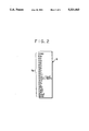
- FIG. 2 schematically shows an interface connector of the memory card
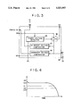
- FIG. 3 is a block diagram showing the circuitry of the power controller of the memory card
- FIG. 4 is a graph showing a discharge curve of the backup battery
- FIG. 5 is a time chart of the data read process from the memory card.
- FIG. 6 is a block diagram showing a power controller according to another embodiment of the present invention.
- a memory card 2 has an interface connector 5 including an I/0 interface and 20 terminals 5a.
- the connector terminals 5a include ground terminals "GND”, a power terminal “Vcc”, 8-bits of data input-output terminals "D0-D7", control terminals "A0-A1", a read terminal "RD”, a write terminal “WR”, a write protect terminal “WP”, a battery check terminal “Vbat” for outputting data indicative of whether the voltage of a backup battery of the memory card 2 is less than a first reference voltage V1, and so forth.
- the battery check terminal Vbat, the power terminal Vcc, and the ground terminals GND are connected to first, second and third terminals S1 to S3 of a power controller 8, respectively.
- the data input-output terminals D0-D7, the control terminals A0 and A1, read terminal RD, the write terminal WR and other terminals are connected to a control circuit 7 through a bus line.
- the control circuit 7 controls data input and output, and is connected to a memory 10 through a control line 9a, an address line 9b and a data line 9c for writing and reading data into and from the memory 10.
- a backup battery 12 is mounted in the memory card 2. It is to be noted that a voltage higher than the backup voltage, e.g. about 5V should be applied to the memory 10 so as to write data therein.
- the higher voltage is applied by an external device to the power controller 8 through the power terminal Vcc of the connector 5.
- the power controller 8, which controls power supply to the memory 10, is configured as shown in FIG. 3.
- the voltage applied at the power terminal Vcc is applied to the power controller 8 through the second terminal S2.
- a power voltage detector 15 switches over a switch 16 to a position shown by a solid line.
- the memory 10 is supplied with the voltage from the external device. So long as no voltage is applied at the second terminal S2, the switch 16 is changed over to another position shown by a dotted line, so that the memory 10 is supplied by the backup battery 12 connected to a fifth terminal S5.
- the third terminal S3 is also connected to the negative pole of the backup battery 12.
- the backup battery 12 is, for example, a coin-shaped lithium battery rated at 3V.
- the discharge curve of the backup battery is shown in FIG. 4.
- First and second backup voltage comparators 17 and 18 compare the momentary voltage of the backup battery 12 with the first reference voltage V1 and a second reference voltage V2 for outputting first and second check signals, respectively.
- the first check signal is at a high level (H) when the backup voltage is equal to or more than the first reference voltage V1, and at a low level (L) when the backup voltage is less than the voltage V1.
- the second check signal is at a high level (H) when the backup voltage is equal to or more than the second reference voltage V2, and at a low level (L) when the backup voltage is less than the voltage V2.
- the first check signal is sent to the control circuit 7 through a sixth terminal S6.
- the control circuit 7 outputs the first check signal to an external device through one of the data input-output terminals D1-D7, for instance the terminal D7, while the second check signal is sent to the external device through the first terminal S1 and the battery check terminal Vbat.
- the first reference voltage V1 is higher than the second reference voltage V2 as shown in FIG. 4, and both reference voltages V1 and V2 are higher than the voltage necessary for preserving data in the memory 10, for instance, 2V.
- the first reference voltage V1 is set at such a level that the backup battery 12 will be discharged from this level V1 to "2V" in a relatively long time, e.g. several weeks.
- the reference voltage V2 is set at such a level that the backup battery 12 will be discharged from this level V2 to "2V" in a shorter time, e.g. several days. Accordingly, the backup battery 12 should be replaced by a new one if the backup voltage is determined to be lower than the second reference voltage V2.
- the memory card 12 of this embodiment is used as an external recording medium for an electronic still camera 20, as shown in FIG. 1.
- the electronic still camera 20 includes an imaging section 21 including of an optical system, a solid state image sensor and so forth for detecting opt-electronic image signal, and a video signal processor 22 for converting the opt-electronic signal into an NTSC video signal.
- the video signal from the video signal processor 22 is, after converted into a digital signal by a control circuit 24, sent to the memory card 2 through an interface connector 25.
- the interface connector 25 includes an I/0 interface and a group of terminals 25a. that may be connected to the terminals 5a of the memory card 2.
- the electronic still camera 20 has a power source battery 26 therein, which supplies the respective circuit block of the electronic still camera 20.
- the battery 26 also supplies the memory card 2 through the power terminal Vcc when writing to the memory 10.
- the battery check circuit 27 determines whether the voltage of the power source battery 26 is more than a predetermined level.
- the battery check circuit 27 also checks the condition of the backup battery 2, of the memory card 12, on the basis of the second check signal output from the battery check terminal Vbat and the first check signal output from the data terminal D7 which is ordinarily used for data communication between the camera 20 and the memory card 2. Green, yellow and red LEDs 30, 31 and 32 are provided to indicate the result of the battery checking.
- the voltage of the power source battery 26 of the camera 20 is applied to the terminal S2 of the power control circuit 8 through the power terminal Vcc by turning a power switch of the electronic still camera on.
- the power voltage detector 15 changes over the switch 16 to the position shown by the solid line upon detection of the voltage from the power source battery 26 which enables data to be written in the memory 10.
- the control circuit 24 of the camera 20 when the power switch of the electronic still camera 20 is turned on at a time T1, the control circuit 24 of the camera 20 outputs a H signal to the read terminal RD of the memory card 2 for setting the memory card 2 to a read mode.
- the camera 20 In the read mode, the camera 20 outputs a binary signal "0, 0" as a control signal to control terminals A0 and A1 of the memory card 2.
- the control circuit 7 of the memory card 2 outputs card type data SD1 to the camera 20 through the data terminals D0-D3, during a period from T1 to T2 in FIG. 5.
- the card type data SD1 indicates the type of memory 10.
- the data terminal D0 is assigned to output data indicative of whether the memory 10 includes a RAM
- the data terminal D1 indicates whether the memory 10 includes a Mask ROM
- the terminal D2 indicates whether the memory 10 includes a PROM
- the data terminal D3 indicates whether the memory 10 includes a EEPROM.
- Other data terminals D4-D7 are not used to output the card type data.
- the voltage of the backup battery 12 is compared with the reference voltages V1 and V2 in the backup voltage comparators 17 and 18.
- the first battery check signal from the first comparator 17 is sent to the control circuit 7 through the terminal S6, whereas the second battery check signal from the second comparator 18 is output to the electronic still camera 20 through the terminal S1 and the battery check terminal Vbat. Because the data terminals D4-D7 are not used during, the period T1-T2, the control circuit 7 controls the output of the first battery check signal to the camera 20 through the data terminal D7 during this period.
- the control circuit 24 of the camera 20 discriminates the type of the memory 10 based on the card type data SD1, so as to set the camera 20 at a corresponding read-write control mode. It is possible to display the type of the memory card 2.
- the control circuit 24 also send the first and second battery check signals to the battery check circuit 27.
- the battery check circuit 27 firstly determines whether the power battery 26 in the electronic still camera 20 is consumed. If the voltage of the power battery 26 is less than a predetermined level, the battery check circuit 27 causes the red LED 32 to emit. If the voltage of the power battery 26 is not less than the predetermined level, then it is determined whether the voltage of the backup battery 12 of the memory card 2 is sufficient for preserving video data in the memory 10. If the backup battery 12 is new and hence the voltage thereof is equal to or more than the reference voltage V1, the battery check signals from the first and second backup voltage comparators 17 and 18 are at the H level, so that the battery check circuit 27 causes the green LED 30 to emit. In this way, the operator can see that both the power battery 26 and the backup battery 12 have sufficient levels of voltage.
- the first check signal is at the H level, whereas the second check signal is at the L level.
- the battery check circuit 27 causes the yellow LED 31 to emit, so as to indicate that the voltage of the backup battery 12 is critical and will be consumed within several weeks. Then, the operator only has to replace the backup battery 12 with a new battery within several weeks. Namely, the operator does not need to prepare a spare battery as rapidly to replace the backup battery 12.
- both the first and second check signals are at the L level. Then, the battery check circuit 27 causes the red LED 32 to emit, thereby alarming that the video data written in the memory card 2 will vanish in several days. As a result, the operator must replace the battery 12 by a new battery soon as possible.
- the control circuit 24 When the voltage of the power battery 26 and the voltage of the backup battery 12 are determined to be sufficient, the control circuit 24 outputs a binary signal "1, 0" as a control signal to the control terminals A0 and A1 of the memory card 2 at a timing T2 shown in FIG. 5. Then, the control circuit 7 of the memory card 2 outputs 8-bit memory capacity data SD2 through the data terminals D0-D7.
- the memory capacity data SD2 indicates the capacity of the memory 10 which is available for writing new video data.
- the control circuit 24 of the camera 20 reads the memory capacity data SD2 in a period of time from T2 and T3, and writes the data SD2 in a memory at a predetermined address of the camera 20. It may be possible to provide a liquid crystal display for displaying the number of frames recordable in the memory card in accordance with the memory capacity data SD2.
- the power supply to the power terminal Vcc is terminated, and the power voltage detector 15 changes over the switch 16 to the position show by dotted line. Then, the memory 10 is supplied by the backup battery 12, so as to preserve the data written in the memory 10 without an external power supply.
- FIG. 6 shows another embodiment of the present invention, wherein like or similar parts are designated by the same reference numerals used in FIG. 1.
- the second check signal which is output at the terminal S1 of the power controller 8 is sent to a control circuit 36 rather than the battery check terminal Vbat.
- the control circuit 36 controls the output of the first and second check signals through the data terminals D6 and D7 while outputting the above-described card type data SD1 through the data terminals D0-D3 in a period of time from T1 to T2 as shown in FIG. 5.
- the terminals which would otherwise be used as a battery voltage check terminal Vbat is an empty terminal Dx, it becomes possible to use this empty terminal Dx for another function.
- this empty terminal Dx may be used as a further control terminal necessary for an upgraded version of the memory card. In this way, the memory card can have a supplemental function.
- the first check signal is not necessarily read out concurrently with the reading of the card type data SD1 from the memory card 2. Rather, the first check signal may be read out at another time only if at least one of the data terminals D0-D7 is not occupied at that time. It is possible to display the condition of the backup battery 12 and the power battery 20 on a liquid crystal display in place of the LEDs 30 to 32. It is also possible to compare the backup voltage with more than two reference voltages so as to check the backup battery 12 more elaborately, wherein the number of reference voltages depends on the number of unused data terminals D0-D7, that is, the bits of the data that should be sent concurrently with the battery check signals.
- the memory card of the present invention may be adapted for use not only in audio or video recording devices, but also in any other device which has data processing functions.
Landscapes
- Engineering & Computer Science (AREA)
- Power Engineering (AREA)
- Power Sources (AREA)
- Credit Cards Or The Like (AREA)
- Techniques For Improving Reliability Of Storages (AREA)
Applications Claiming Priority (2)
| Application Number | Priority Date | Filing Date | Title |
|---|---|---|---|
| JP3-53870 | 1991-02-25 | ||
| JP3053870A JPH04268990A (ja) | 1991-02-25 | 1991-02-25 | メモリカード |
Publications (1)
| Publication Number | Publication Date |
|---|---|
| US5321663A true US5321663A (en) | 1994-06-14 |
Family
ID=12954792
Family Applications (1)
| Application Number | Title | Priority Date | Filing Date |
|---|---|---|---|
| US07/838,828 Expired - Lifetime US5321663A (en) | 1991-02-25 | 1992-02-21 | Memory card and method and apparatus for checking backup voltage of memory card |
Country Status (2)
| Country | Link |
|---|---|
| US (1) | US5321663A (ja) |
| JP (1) | JPH04268990A (ja) |
Cited By (10)
| Publication number | Priority date | Publication date | Assignee | Title |
|---|---|---|---|---|
| US5798961A (en) * | 1994-08-23 | 1998-08-25 | Emc Corporation | Non-volatile memory module |
| US5831351A (en) * | 1995-06-09 | 1998-11-03 | Dell Usa L.P. | Method and apparatus for self shutdown of a battery-backed circuit card |
| US6415391B1 (en) * | 1994-09-22 | 2002-07-02 | Nec Corporation | Control method and system for resetting backup data |
| US20030198035A1 (en) * | 2002-04-22 | 2003-10-23 | Adc Dsl Systems, Inc. | Circuit cards having a single ground plane with logic devices connected thereto |
| US20040193955A1 (en) * | 2003-03-31 | 2004-09-30 | Leete Brian A. | Computer memory power backup |
| US20050104977A1 (en) * | 2002-01-11 | 2005-05-19 | Nikon Corporation | Digital camera |
| US20060242344A1 (en) * | 2005-04-11 | 2006-10-26 | Murata Kikai Kabushiki Kaisha | Electronic device to which memory module can be added |
| US20080211927A1 (en) * | 2002-02-18 | 2008-09-04 | Nikon Corporation | Digital camera |
| US20090273315A1 (en) * | 1998-09-29 | 2009-11-05 | Nguyen Don J | Method and apparatus for battery pre-check at system power-on |
| US20140380067A1 (en) * | 2013-06-19 | 2014-12-25 | Western Digital Technologies, Inc. | Backup power for reducing host current transients |
Families Citing this family (4)
| Publication number | Priority date | Publication date | Assignee | Title |
|---|---|---|---|---|
| JP4600517B2 (ja) * | 2008-05-09 | 2010-12-15 | 株式会社ニコン | デジタルカメラ |
| JP4600565B2 (ja) * | 2008-10-02 | 2010-12-15 | 株式会社ニコン | デジタルカメラ |
| JP2016192068A (ja) * | 2015-03-31 | 2016-11-10 | 三菱電機エンジニアリング株式会社 | 交通事故自動記録装置 |
| JP2019211383A (ja) * | 2018-06-07 | 2019-12-12 | Necパーソナルコンピュータ株式会社 | 電子機器 |
Citations (5)
| Publication number | Priority date | Publication date | Assignee | Title |
|---|---|---|---|---|
| US4654829A (en) * | 1984-12-17 | 1987-03-31 | Dallas Semiconductor Corporation | Portable, non-volatile read/write memory module |
| US4662736A (en) * | 1984-12-29 | 1987-05-05 | Minolta Camera Kabushiki Kaisha | Power supply system for memory unit of camera |
| US4908790A (en) * | 1988-03-10 | 1990-03-13 | Dallas Semiconductor Corporation | Backup battery switching circuitry for a microcomputer or a microprocessor |
| US4985870A (en) * | 1986-07-02 | 1991-01-15 | Dallas Semiconductor Corporation | Apparatus for connecting electronic modules containing integrated circuits and backup batteries |
| US5007027A (en) * | 1988-05-16 | 1991-04-09 | Fujitsu Limited | Data protection system in a data processing system |
-
1991
- 1991-02-25 JP JP3053870A patent/JPH04268990A/ja active Pending
-
1992
- 1992-02-21 US US07/838,828 patent/US5321663A/en not_active Expired - Lifetime
Patent Citations (5)
| Publication number | Priority date | Publication date | Assignee | Title |
|---|---|---|---|---|
| US4654829A (en) * | 1984-12-17 | 1987-03-31 | Dallas Semiconductor Corporation | Portable, non-volatile read/write memory module |
| US4662736A (en) * | 1984-12-29 | 1987-05-05 | Minolta Camera Kabushiki Kaisha | Power supply system for memory unit of camera |
| US4985870A (en) * | 1986-07-02 | 1991-01-15 | Dallas Semiconductor Corporation | Apparatus for connecting electronic modules containing integrated circuits and backup batteries |
| US4908790A (en) * | 1988-03-10 | 1990-03-13 | Dallas Semiconductor Corporation | Backup battery switching circuitry for a microcomputer or a microprocessor |
| US5007027A (en) * | 1988-05-16 | 1991-04-09 | Fujitsu Limited | Data protection system in a data processing system |
Cited By (18)
| Publication number | Priority date | Publication date | Assignee | Title |
|---|---|---|---|---|
| US5798961A (en) * | 1994-08-23 | 1998-08-25 | Emc Corporation | Non-volatile memory module |
| US6415391B1 (en) * | 1994-09-22 | 2002-07-02 | Nec Corporation | Control method and system for resetting backup data |
| US5831351A (en) * | 1995-06-09 | 1998-11-03 | Dell Usa L.P. | Method and apparatus for self shutdown of a battery-backed circuit card |
| US20110133745A1 (en) * | 1998-09-29 | 2011-06-09 | Nguyen Don J | Method and apparatus for battery power pre-check at system power-on |
| US7888943B2 (en) * | 1998-09-29 | 2011-02-15 | Intel Corporation | Method and apparatus for battery test |
| US20090273315A1 (en) * | 1998-09-29 | 2009-11-05 | Nguyen Don J | Method and apparatus for battery pre-check at system power-on |
| US8681243B2 (en) | 2002-01-11 | 2014-03-25 | Nikon Corporation | Digital camera |
| US20050104977A1 (en) * | 2002-01-11 | 2005-05-19 | Nikon Corporation | Digital camera |
| US20080211927A1 (en) * | 2002-02-18 | 2008-09-04 | Nikon Corporation | Digital camera |
| US8149295B2 (en) | 2002-02-18 | 2012-04-03 | Nikon Corporation | Digital camera with external storage medium detector |
| US8659677B2 (en) | 2002-02-18 | 2014-02-25 | Nikon Corporation | Digital camera with external storage medium detector |
| US6819571B2 (en) * | 2002-04-22 | 2004-11-16 | Adc Dsl Systems, Inc. | Circuit cards having a single ground plane with logic devices connected thereto |
| US20030198035A1 (en) * | 2002-04-22 | 2003-10-23 | Adc Dsl Systems, Inc. | Circuit cards having a single ground plane with logic devices connected thereto |
| US7836339B2 (en) * | 2003-03-31 | 2010-11-16 | Intel Corporation | Computer memory power backup |
| US20040193955A1 (en) * | 2003-03-31 | 2004-09-30 | Leete Brian A. | Computer memory power backup |
| US20060242344A1 (en) * | 2005-04-11 | 2006-10-26 | Murata Kikai Kabushiki Kaisha | Electronic device to which memory module can be added |
| US20140380067A1 (en) * | 2013-06-19 | 2014-12-25 | Western Digital Technologies, Inc. | Backup power for reducing host current transients |
| US9304560B2 (en) * | 2013-06-19 | 2016-04-05 | Western Digital Technologies, Inc. | Backup power for reducing host current transients |
Also Published As
| Publication number | Publication date |
|---|---|
| JPH04268990A (ja) | 1992-09-24 |
Similar Documents
| Publication | Publication Date | Title |
|---|---|---|
| US5321663A (en) | Memory card and method and apparatus for checking backup voltage of memory card | |
| US4916662A (en) | IC card including high input voltage detection and suppression | |
| US5093731A (en) | Image data recording apparatus for storing image data with a recording-finished code and a recording sequence code | |
| EP0528280B1 (en) | Memory card apparatus | |
| US5745912A (en) | Memory card apparatus including a link table for managing the correspondency between the recorded contents in the memory card and that in the link table | |
| US6118929A (en) | Solid-state camera and solid-state memory apparatus | |
| JPH06332580A (ja) | メモリカード制御装置 | |
| US7478260B2 (en) | System and method for setting a clock rate in a memory card | |
| US5418926A (en) | System and method for indicating whether a block size in a detachable memory device corresponds to a predetermined broadcasting system standard | |
| EP0557968B1 (en) | Method of rewriting data in EEPROM, and EEPROM card | |
| US20080084487A1 (en) | Imaging apparatus, imaging pickup unit connectable to a lens unit, and a lens unit connectable to imaging pickup unit | |
| US5761061A (en) | Data processing medium, its backup circuit, and data processing system | |
| EP0890955A2 (en) | Storage apparatus, data write-in method, and data read-out method | |
| US6816190B1 (en) | Electronic camera having a plurality of storage media | |
| EP0862080B1 (en) | Image recording and reproducing apparatus | |
| US6850270B1 (en) | Electronic camera with built-in printer | |
| KR20030051407A (ko) | 반도체 장치, 불휘발성 반도체 기억 장치, 반도체 장치또는 불휘발성 반도체 기억 장치를 복수 포함하는 시스템,반도체 장치 또는 불휘발성 반도체 기억 장치를 포함하는전자 카드, 이 전자 카드의 사용이 가능한 전자 장치 | |
| US5821996A (en) | Solid-sate camera with solid-state memory for holding characteristic code representing characteristic of an internal circuit | |
| JP2011118768A (ja) | 電子機器 | |
| JP3537838B2 (ja) | メモリカード制御方法およびシステム | |
| JPH07225687A (ja) | 電子スチルカメラ | |
| JPH0658618B2 (ja) | メモリ装置 | |
| JPH07320017A (ja) | Icメモリカード | |
| JP3532614B2 (ja) | メモリパックおよび電子機器 | |
| JP3528058B2 (ja) | デジタルスチルカメラ |
Legal Events
| Date | Code | Title | Description |
|---|---|---|---|
| AS | Assignment |
Owner name: FUJI PHOTO FILM CO., LTD., JAPAN Free format text: ASSIGNMENT OF ASSIGNORS INTEREST.;ASSIGNOR:NISHI, SEIKI;REEL/FRAME:006076/0128 Effective date: 19920313 |
|
| STCF | Information on status: patent grant |
Free format text: PATENTED CASE |
|
| FPAY | Fee payment |
Year of fee payment: 4 |
|
| FPAY | Fee payment |
Year of fee payment: 8 |
|
| FEPP | Fee payment procedure |
Free format text: PAYOR NUMBER ASSIGNED (ORIGINAL EVENT CODE: ASPN); ENTITY STATUS OF PATENT OWNER: LARGE ENTITY |
|
| FPAY | Fee payment |
Year of fee payment: 12 |
|
| AS | Assignment |
Owner name: FUJIFILM HOLDINGS CORPORATION, JAPAN Free format text: CHANGE OF NAME;ASSIGNOR:FUJI PHOTO FILM CO., LTD.;REEL/FRAME:018898/0872 Effective date: 20061001 Owner name: FUJIFILM HOLDINGS CORPORATION,JAPAN Free format text: CHANGE OF NAME;ASSIGNOR:FUJI PHOTO FILM CO., LTD.;REEL/FRAME:018898/0872 Effective date: 20061001 |
|
| AS | Assignment |
Owner name: FUJIFILM CORPORATION, JAPAN Free format text: ASSIGNMENT OF ASSIGNORS INTEREST;ASSIGNOR:FUJIFILM HOLDINGS CORPORATION;REEL/FRAME:018934/0001 Effective date: 20070130 Owner name: FUJIFILM CORPORATION,JAPAN Free format text: ASSIGNMENT OF ASSIGNORS INTEREST;ASSIGNOR:FUJIFILM HOLDINGS CORPORATION;REEL/FRAME:018934/0001 Effective date: 20070130 |