US5438484A - Surface lighting device and a display having such a lighting device - Google Patents
Surface lighting device and a display having such a lighting device Download PDFInfo
- Publication number
- US5438484A US5438484A US07/984,836 US98483692A US5438484A US 5438484 A US5438484 A US 5438484A US 98483692 A US98483692 A US 98483692A US 5438484 A US5438484 A US 5438484A
- Authority
- US
- United States
- Prior art keywords
- light
- light guide
- surface lighting
- lighting device
- divided
- Prior art date
- Legal status (The legal status is an assumption and is not a legal conclusion. Google has not performed a legal analysis and makes no representation as to the accuracy of the status listed.)
- Expired - Lifetime
Links
- 238000009792 diffusion process Methods 0.000 claims description 51
- 239000004973 liquid crystal related substance Substances 0.000 claims description 25
- 238000003466 welding Methods 0.000 claims description 10
- 239000000463 material Substances 0.000 claims description 9
- 239000004033 plastic Substances 0.000 claims description 7
- 239000000853 adhesive Substances 0.000 claims description 6
- 230000001070 adhesive effect Effects 0.000 claims description 6
- 239000004925 Acrylic resin Substances 0.000 claims description 5
- 229920000178 Acrylic resin Polymers 0.000 claims description 5
- 239000011521 glass Substances 0.000 claims description 5
- 230000004907 flux Effects 0.000 description 21
- 230000002441 reversible effect Effects 0.000 description 10
- 239000002184 metal Substances 0.000 description 8
- 238000009434 installation Methods 0.000 description 7
- 230000000694 effects Effects 0.000 description 5
- 238000005286 illumination Methods 0.000 description 5
- 238000000034 method Methods 0.000 description 5
- 241001247986 Calotropis procera Species 0.000 description 3
- 230000006866 deterioration Effects 0.000 description 3
- 238000005476 soldering Methods 0.000 description 3
- 230000002411 adverse Effects 0.000 description 2
- 239000004020 conductor Substances 0.000 description 2
- 230000004438 eyesight Effects 0.000 description 2
- 230000020169 heat generation Effects 0.000 description 2
- 230000003287 optical effect Effects 0.000 description 2
- 238000012360 testing method Methods 0.000 description 2
- 229910000906 Bronze Inorganic materials 0.000 description 1
- OAICVXFJPJFONN-UHFFFAOYSA-N Phosphorus Chemical compound [P] OAICVXFJPJFONN-UHFFFAOYSA-N 0.000 description 1
- 238000013459 approach Methods 0.000 description 1
- 230000002238 attenuated effect Effects 0.000 description 1
- 230000005540 biological transmission Effects 0.000 description 1
- 239000010974 bronze Substances 0.000 description 1
- 230000008859 change Effects 0.000 description 1
- 238000004040 coloring Methods 0.000 description 1
- 230000001143 conditioned effect Effects 0.000 description 1
- KUNSUQLRTQLHQQ-UHFFFAOYSA-N copper tin Chemical compound [Cu].[Sn] KUNSUQLRTQLHQQ-UHFFFAOYSA-N 0.000 description 1
- 238000005520 cutting process Methods 0.000 description 1
- 230000002950 deficient Effects 0.000 description 1
- 238000009826 distribution Methods 0.000 description 1
- 238000005562 fading Methods 0.000 description 1
- 230000006872 improvement Effects 0.000 description 1
- 238000003780 insertion Methods 0.000 description 1
- 230000037431 insertion Effects 0.000 description 1
- 238000011900 installation process Methods 0.000 description 1
- 230000001678 irradiating effect Effects 0.000 description 1
- 238000005304 joining Methods 0.000 description 1
- 239000007788 liquid Substances 0.000 description 1
- 230000007774 longterm Effects 0.000 description 1
- 238000003754 machining Methods 0.000 description 1
- 238000012423 maintenance Methods 0.000 description 1
- 238000012986 modification Methods 0.000 description 1
- 230000004048 modification Effects 0.000 description 1
- 238000000465 moulding Methods 0.000 description 1
- 238000003825 pressing Methods 0.000 description 1
- 230000008569 process Effects 0.000 description 1
- 230000002035 prolonged effect Effects 0.000 description 1
- 230000009467 reduction Effects 0.000 description 1
- 239000004065 semiconductor Substances 0.000 description 1
- 239000007787 solid Substances 0.000 description 1
Images




Classifications
-
- G—PHYSICS
- G02—OPTICS
- G02B—OPTICAL ELEMENTS, SYSTEMS OR APPARATUS
- G02B6/00—Light guides; Structural details of arrangements comprising light guides and other optical elements, e.g. couplings
- G02B6/0001—Light guides; Structural details of arrangements comprising light guides and other optical elements, e.g. couplings specially adapted for lighting devices or systems
- G02B6/0011—Light guides; Structural details of arrangements comprising light guides and other optical elements, e.g. couplings specially adapted for lighting devices or systems the light guides being planar or of plate-like form
- G02B6/0033—Means for improving the coupling-out of light from the light guide
- G02B6/005—Means for improving the coupling-out of light from the light guide provided by one optical element, or plurality thereof, placed on the light output side of the light guide
- G02B6/0051—Diffusing sheet or layer
-
- G—PHYSICS
- G02—OPTICS
- G02B—OPTICAL ELEMENTS, SYSTEMS OR APPARATUS
- G02B6/00—Light guides; Structural details of arrangements comprising light guides and other optical elements, e.g. couplings
- G02B6/0001—Light guides; Structural details of arrangements comprising light guides and other optical elements, e.g. couplings specially adapted for lighting devices or systems
- G02B6/0011—Light guides; Structural details of arrangements comprising light guides and other optical elements, e.g. couplings specially adapted for lighting devices or systems the light guides being planar or of plate-like form
- G02B6/0033—Means for improving the coupling-out of light from the light guide
- G02B6/005—Means for improving the coupling-out of light from the light guide provided by one optical element, or plurality thereof, placed on the light output side of the light guide
- G02B6/0055—Reflecting element, sheet or layer
-
- G—PHYSICS
- G02—OPTICS
- G02B—OPTICAL ELEMENTS, SYSTEMS OR APPARATUS
- G02B6/00—Light guides; Structural details of arrangements comprising light guides and other optical elements, e.g. couplings
- G02B6/0001—Light guides; Structural details of arrangements comprising light guides and other optical elements, e.g. couplings specially adapted for lighting devices or systems
- G02B6/0011—Light guides; Structural details of arrangements comprising light guides and other optical elements, e.g. couplings specially adapted for lighting devices or systems the light guides being planar or of plate-like form
- G02B6/0066—Light guides; Structural details of arrangements comprising light guides and other optical elements, e.g. couplings specially adapted for lighting devices or systems the light guides being planar or of plate-like form characterised by the light source being coupled to the light guide
- G02B6/007—Incandescent lamp or gas discharge lamp
- G02B6/0071—Incandescent lamp or gas discharge lamp with elongated shape, e.g. tube
-
- G—PHYSICS
- G02—OPTICS
- G02B—OPTICAL ELEMENTS, SYSTEMS OR APPARATUS
- G02B6/00—Light guides; Structural details of arrangements comprising light guides and other optical elements, e.g. couplings
- G02B6/0001—Light guides; Structural details of arrangements comprising light guides and other optical elements, e.g. couplings specially adapted for lighting devices or systems
- G02B6/0011—Light guides; Structural details of arrangements comprising light guides and other optical elements, e.g. couplings specially adapted for lighting devices or systems the light guides being planar or of plate-like form
- G02B6/0081—Mechanical or electrical aspects of the light guide and light source in the lighting device peculiar to the adaptation to planar light guides, e.g. concerning packaging
- G02B6/0086—Positioning aspects
- G02B6/009—Positioning aspects of the light source in the package
-
- G—PHYSICS
- G09—EDUCATION; CRYPTOGRAPHY; DISPLAY; ADVERTISING; SEALS
- G09F—DISPLAYING; ADVERTISING; SIGNS; LABELS OR NAME-PLATES; SEALS
- G09F13/00—Illuminated signs; Luminous advertising
- G09F13/04—Signs, boards or panels, illuminated from behind the insignia
- G09F13/0409—Arrangements for homogeneous illumination of the display surface, e.g. using a layer having a non-uniform transparency
-
- G—PHYSICS
- G09—EDUCATION; CRYPTOGRAPHY; DISPLAY; ADVERTISING; SEALS
- G09F—DISPLAYING; ADVERTISING; SIGNS; LABELS OR NAME-PLATES; SEALS
- G09F13/00—Illuminated signs; Luminous advertising
- G09F13/04—Signs, boards or panels, illuminated from behind the insignia
- G09F13/0418—Constructional details
- G09F13/0454—Slidable panels or parts
-
- G—PHYSICS
- G02—OPTICS
- G02B—OPTICAL ELEMENTS, SYSTEMS OR APPARATUS
- G02B6/00—Light guides; Structural details of arrangements comprising light guides and other optical elements, e.g. couplings
- G02B6/0001—Light guides; Structural details of arrangements comprising light guides and other optical elements, e.g. couplings specially adapted for lighting devices or systems
- G02B6/0011—Light guides; Structural details of arrangements comprising light guides and other optical elements, e.g. couplings specially adapted for lighting devices or systems the light guides being planar or of plate-like form
- G02B6/0013—Means for improving the coupling-in of light from the light source into the light guide
- G02B6/0023—Means for improving the coupling-in of light from the light source into the light guide provided by one optical element, or plurality thereof, placed between the light guide and the light source, or around the light source
- G02B6/0026—Wavelength selective element, sheet or layer, e.g. filter or grating
-
- G—PHYSICS
- G02—OPTICS
- G02B—OPTICAL ELEMENTS, SYSTEMS OR APPARATUS
- G02B6/00—Light guides; Structural details of arrangements comprising light guides and other optical elements, e.g. couplings
- G02B6/0001—Light guides; Structural details of arrangements comprising light guides and other optical elements, e.g. couplings specially adapted for lighting devices or systems
- G02B6/0011—Light guides; Structural details of arrangements comprising light guides and other optical elements, e.g. couplings specially adapted for lighting devices or systems the light guides being planar or of plate-like form
- G02B6/0033—Means for improving the coupling-out of light from the light guide
- G02B6/0035—Means for improving the coupling-out of light from the light guide provided on the surface of the light guide or in the bulk of it
- G02B6/0045—Means for improving the coupling-out of light from the light guide provided on the surface of the light guide or in the bulk of it by shaping at least a portion of the light guide
- G02B6/0046—Tapered light guide, e.g. wedge-shaped light guide
-
- G—PHYSICS
- G02—OPTICS
- G02B—OPTICAL ELEMENTS, SYSTEMS OR APPARATUS
- G02B6/00—Light guides; Structural details of arrangements comprising light guides and other optical elements, e.g. couplings
- G02B6/0001—Light guides; Structural details of arrangements comprising light guides and other optical elements, e.g. couplings specially adapted for lighting devices or systems
- G02B6/0011—Light guides; Structural details of arrangements comprising light guides and other optical elements, e.g. couplings specially adapted for lighting devices or systems the light guides being planar or of plate-like form
- G02B6/0033—Means for improving the coupling-out of light from the light guide
- G02B6/0058—Means for improving the coupling-out of light from the light guide varying in density, size, shape or depth along the light guide
- G02B6/0061—Means for improving the coupling-out of light from the light guide varying in density, size, shape or depth along the light guide to provide homogeneous light output intensity
-
- G—PHYSICS
- G02—OPTICS
- G02B—OPTICAL ELEMENTS, SYSTEMS OR APPARATUS
- G02B6/00—Light guides; Structural details of arrangements comprising light guides and other optical elements, e.g. couplings
- G02B6/0001—Light guides; Structural details of arrangements comprising light guides and other optical elements, e.g. couplings specially adapted for lighting devices or systems
- G02B6/0011—Light guides; Structural details of arrangements comprising light guides and other optical elements, e.g. couplings specially adapted for lighting devices or systems the light guides being planar or of plate-like form
- G02B6/0066—Light guides; Structural details of arrangements comprising light guides and other optical elements, e.g. couplings specially adapted for lighting devices or systems the light guides being planar or of plate-like form characterised by the light source being coupled to the light guide
- G02B6/0068—Arrangements of plural sources, e.g. multi-colour light sources
-
- G—PHYSICS
- G09—EDUCATION; CRYPTOGRAPHY; DISPLAY; ADVERTISING; SEALS
- G09F—DISPLAYING; ADVERTISING; SIGNS; LABELS OR NAME-PLATES; SEALS
- G09F13/00—Illuminated signs; Luminous advertising
- G09F13/18—Edge-illuminated signs
- G09F2013/1804—Achieving homogeneous illumination
- G09F2013/1827—Prismatic window
-
- G—PHYSICS
- G09—EDUCATION; CRYPTOGRAPHY; DISPLAY; ADVERTISING; SEALS
- G09F—DISPLAYING; ADVERTISING; SIGNS; LABELS OR NAME-PLATES; SEALS
- G09F13/00—Illuminated signs; Luminous advertising
- G09F13/18—Edge-illuminated signs
- G09F2013/1804—Achieving homogeneous illumination
- G09F2013/1831—Achieving homogeneous illumination using more than one light source
-
- Y—GENERAL TAGGING OF NEW TECHNOLOGICAL DEVELOPMENTS; GENERAL TAGGING OF CROSS-SECTIONAL TECHNOLOGIES SPANNING OVER SEVERAL SECTIONS OF THE IPC; TECHNICAL SUBJECTS COVERED BY FORMER USPC CROSS-REFERENCE ART COLLECTIONS [XRACs] AND DIGESTS
- Y10—TECHNICAL SUBJECTS COVERED BY FORMER USPC
- Y10S—TECHNICAL SUBJECTS COVERED BY FORMER USPC CROSS-REFERENCE ART COLLECTIONS [XRACs] AND DIGESTS
- Y10S385/00—Optical waveguides
- Y10S385/901—Illuminating or display apparatus
Definitions
- the present invention relates to a surface lighting device and a display having such a lighting device. More particularly, the invention relates to a surface lighting device preferably used for a backlight device for backlighting a liquid crystal display and other displaying apparatuses, and a display having such a surface lighting device.
- a surface lighting device is capable of emitting light evenly over a wide area. It is thus applicable as various lighting means.
- a liquid crystal itself does not emit any light in the liquid crystal display or the like, it is usually practiced to light up the liquid crystal panel from its rear side using a light source in order to improve the display conditions for an easier observation of the displayed images.
- a desirable surface lighting device serving as a backlight source of the kind it is required and the luminance is even for the light emitting surface, that is, at least the area corresponding to the entire display surface of the display, and that the apparatus is small and light in weight as well as the lighting efficiency is high for its power consumption.
- this surface lighting device when adopted as a display, its mode should preferably be such that the display can be fabricated thin as a whole.
- the surface light device of an edge type using semiconductors As a surface light device which can satisfy such requirements, there is known the surface light device of an edge type using semiconductors, and as a display having such a surface lighting device, there is known the display which is represented in a schematically cross-sectional view in FIG. 1.
- reference numerals 1a and 1b designate light sources; 2, a reflection board; 3, a diffusion board; 4, a light guide; 5, a liquid crystal display panel; 6, an outer housing; and 8, a diffusion reflection pattern.
- FIG. 2 is a plan view schematically showing a surface lighting device used for the display shown in FIG. 1, which is observed from the light emitting side (from the side where the liquid crystal display panel is mounted).
- a reference numeral 9 designates lamp leads; 10, lamp electrode portions; 11, a lamp emission portion; and 12, the effective emission surface of the surface light device.
- FIG. 1 is a cross-sectional view schematically showing the display taken along 1--1' in FIG. 2.
- the surface lighting device shown in FIG. 1 and FIG. 2 is provided with the light sources 1a and 1b with the light guide 4 therebetween. Also, the diffusion reflection pattern 8 is provided on the side opposite to the light emitting surface of the light guide 4. Then, there is provided the reflection board 2 which has an opening encircling the aforesaid light sources 1a and 1b, light guide 4, and diffusion reflection pattern 8. Also, the diffusion board 3 is arranged above the opening of the reflection board 2. The outer housing 6 is arranged to encircle the reflection board 2 with its opening portion provided corresponding to the opening of the aforesaid reflection board 2.
- the above-mentioned surface lighting device has a transparent member made of a glass or plastic material such as acrylic resin, and the incident rays of light from the light sources 1a and 1b through the sides of the light guide 4 are emitted from the front face of the light guide 4 after being uniformalized through the reflection board 2 and diffusion board 3.
- the light sources 1a and 1b are arranged at both ends of the effective light emission surface 12 to place it between them.
- the luminous fluxes emitted from the light sources 1a and 1b enter the light guide 4 made of transparent acrylic resin or the like. Then, the structure is arranged so as to guide them to the center as much as possible through the reflection pattern portion 8 on the reverse side of the light guide 4 and the reflection board 2.
- the diffusion reflection pattern portion 8 is arranged more densely further away from the light source 1a or 1b. It is thus attempted to guide the incident rays of light to the central portion of the light guide 4.
- FIG. 3 is also a cross-sectional view schematically showing the display having the surface lighting device taken along the same position as FIG. 1.
- the light guide 4 has a curvature on each side of the light sources 1a and 1b to match the configurations of the light sources 1a and 1b. In this way, it is implemented to enable the rays of light from the light sources 1a and 1b to enter the photoconductor more effectively as well as to make the device compact.
- the surface lighting device of an edge type has a low luminance in the central portion between the light sources and a high luminance in the vicinity of the light sources as indicated by a broken line C shown in FIG. 9. This is because the light sources 1a and 1b emit diffusion light and make the vicinity of the light sources 1a and 1b bright while the light emitted from the light sources 1a and 1b mostly reach the opposite light source 1b and 1a to be diffused, respectively, thus making the vicinity of the light sources 1a and 1b brighter.
- the implementation of color display, or a better visivility of display it is conceivable to provide the light sources 1a and 1b not only on one opposing sides of the light guide 4, but also on the other opposing sides thereof. Now, in conjunction with FIG. 5 and FIG. 6, such an example will be described.
- FIG. 5 is a cross-sectional view schematically showing a display as in FIG. 1.
- FIG. 6 is a perspective view schematically showing the relations between the arrangements of the light sources 1a, 1b, 1c, and 1d and the light guide 4.
- FIG. 5 illustrates the display sectionally at a position corresponding to the position taken along 5--5' in FIG. 6.
- the same reference numerals as in FIG. 1 designate the same elements. Here, therefore, descriptions will be omitted for such elements.
- the four light sources 1a to 1d are arranged along the four sides of the light guide 4 in a configuration of a board.
- the luminous flux Z is not related to the diffusion reflection pattern portion 8. This reaches the light source 1b on the opposite side to increase the luminance in the vicinity of the light source 1b. Also, the light flux Y is substantially reflected critically (light fluxes less than the critical angle being totally reflected) on the upper surface of the light guide 4. Thus, this is not related to the diffusion reflection pattern portion 8, either. Therefore, it causes the luminance to be increased likewise in the vicinity of the light source 1b. In other words, in a usual backlight device of an edge type, it is difficult to intensify the luminance in the central portion between the light sources 1a and 1b according to FIG. 5.
- the device is designed to intensify the luminance in the central portion between the light sources 1a and 1b by the application of the diffusion reflection pattern portion 8 provided for the reverse side of the light guide 4.
- the diffusion reflection pattern portion 8 provided for the reverse side of the light guide 4.
- the present invention is designed. It is an object of the invention to provide a surface lighting device of an edge type which can be fabricated thin at a low cost even for a large size with an excellent evenness and efficiency of luminance, and a display having such a surface lighting device.
- FIG. 1, FIG. 3, and FIG. 5 are cross-sectional views schematically showing displays, respectively.
- FIG. 2 is a plan view schematically showing a surface lighting device.
- FIGS. 4A and 4B are cross-sectional views schematically illustrating the relationship between the light guide and light sources, respectively.
- FIG. 6 is a perspective view schematically illustrating the relationship between the light guide and light sources.
- FIG. 7, FIGS. 11A and 11B, FIGS. 12A and 12B, FIGS. 13A and 13B, and FIG. 15 are cross-sectional views schematically illustrating the relationship between the light guide and light sources according to the present invention.
- FIG. 8, FIG. 14, and FIG. 16 are perspective views schematically illustrating the relationship between the light guide and light sources according to the present invention, respectively.
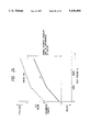
- FIG. 9 is a graph illustrating the luminance characteristics of a surface lighting device.
- FIG. 10 is a graph illustrating the luminance characteristics for the explanation of a surface lighting device according to the present invention.
- FIG. 17, FIG. 19, and FIG. 20 are schematically sectional views for the explanation of light source mountings, respectively.
- FIG. 18 and FIG. 21 are enlarged views for 10 the explanation of the light source mountings, respectively.
- FIG. 22 is a perspective view schematically illustrating another positional relationship between the light emission surface and light sources.
- FIG. 23 is a cross-sectional view schematically illustrating the surface lighting device shown in FIG. 22.
- FIG. 24 is a graph illustrating an example of elapsed time variation of a reflection board.
- FIG. 25 is a schematically sectional view illustrating an example in which a surface light device is applied as a device for backlight source.
- FIG. 26 and FIG. 27 are plan view schematically illustrating the arrangements of light sources for surface lighting device, respectively.
- FIG. 28 is a graph showing the luminance characteristics of the surface lighting device shown in FIG. 26.
- the light guide is divided in a surface lighting device where the rays of light from light sources are allowed to enter the opposing side faces of a transparent light guide and emitted to the front side of the light guide after the incident rays of light are uniformalized through a reflection board and/or a diffusion board according to the present invention.
- FIG. 7 and FIG. 8 are views showing the structure of a liquid crystal backlight device according to a preferable embodiment according to the present invention. Also, FIG. 9 and FIG. 10 represent the luminance characteristics on the surface of a surface lighting device for the explanation of the function of a surface lighting device according to the present invention.
- a light guide 4 is divided in the central portion of the opposing light sources 1a and 1b. Then, the divided portions are bonded by a transparent adhesives 7. With a structure such as this, the luminance on the light emission surface presents the luminance characteristics as indicated by a solid line A in FIG. 9,
- the dotted line B shows the luminance characteristics of a conventional device (V-letter shaped light guide) shown in FIGS. 4A and 4B and the broken line C shows the luminance characteristics of a conventional device (flat light guide) shown in FIG. 1.
- the description will be made of the principle of the present invention.
- the luminous fluxes emitted from the light sources 1a and 1b are allowed to enter a light guide 4 made of a transparent acrylic resin or the like as shown in FIG. 1 and then guided to the central portion through the foregoing light guide 4, a reflection board 2 on the reverse side, and a diffusion reflection pattern portion 8 formed by densifying the portion away from the light sources 1a and 1b.
- a light guide 4 made of a transparent acrylic resin or the like as shown in FIG. 1 and then guided to the central portion through the foregoing light guide 4, a reflection board 2 on the reverse side, and a diffusion reflection pattern portion 8 formed by densifying the portion away from the light sources 1a and 1b.
- its characteristics are such that the luminance close to the light sources becomes high whereas it becomes low in the central portion between the light sources as shown in the characteristics C represented in FIG. 9 for the reasons described earlier.
- FIG. 10 shows the luminance characteristics when the conventional device shown 1 in FIG. 1 and the embodiment of the present invention shown in FIG. 7 are operated respectively without the diffusion reflection patterns 8 on the reverse side of the light guide 4 and only with the light source 1a being illuminated.
- the light guide 4 is divided in the central portion between the opposing light sources 1a and 1b.
- the luminous flux from the light source 1a (illuminated) side is reflected in the vicinity of the divided surface in the aforesaid central portion so as to cause the luminance in the central portion between the light source 1a on the light source 1a side and the divided surface to be intensified, and then, the transmitting light through the aforesaid divided surface enables the luminance in the central portion between the light source 1b on the opposite side and the divided surface to be intensified with the aforesaid divided surface as the secondary light source as represented by the characteristics A shown in FIG.
- the diffusion reflection pattern portion 8 is provided for the reverse side of the light guide 4.
- the density of the diffusion reflection pattern can be optimized by the luminance on the divided surface side which is determined by the optical characteristics of the divided surface such as the luminance and reflection on the light source side, transmission, diffusion, refraction.
- the overall luminance is improved by making the luminance in the central portion between the light sources brighter as represented by the characteristics A shown in FIG. 9.
- the light guide is divided into three, four, or more divisions with the central portion of the light guide as the symmetrical axis.
- the light guide 4 may be possible to divide the light guide 4 in the portions equally away from the central portion of the light guide by a distance a, and the divided portions are bonded by adhesives 7 as shown in FIG. 11A or as shown in FIG. 11B, the light guide 4 is divided respectively in the central portion of the light guide 4 and in the portions equally away from the foregoing central portion by distance a, and these divided portions are bonded by adhesives 7.
- each of them is appropriately set ⁇ 1 in a range of 45 degrees to 90 degrees against the horizontal plane (surface or reverse side) of the light guide 4.
- the divided surfaces are inclined to the surface of the light guide 4 as shown in FIGS. 12A and 12B. Then, the junctions between surfaces are inclined so as to enable the irradiating amount of light to the surface side to be controlled by setting the slanting angle ⁇ 1 appropriately.
- the present invention is applicable to the prior art shown in FIGS. 4A and 4B.
- the central portion of a light guide is provided with a lower recess and an upper recess by the combination of the prior art and the present invention. Then, by bonding the central portions of the light guide 4, it is possible to diffuse and reflect the luminous fluxes further in the vicinity of the foregoing central portions.
- the substantial size of the light guide 4 can be made smaller than that of the light guide which is integrally produced. Accordingly, it becomes possible to make the light guide 4 with a desirable precision even when the surface lighting device is large.
- FIG. 14 is a perspective view schematically showing the structure of a surface lighting device applied as a backlight device to a liquid crystal display according to still another preferable embodiment of the present invention.
- FIG. 15 is a schematically sectional view of a display at a position corresponding to the line taken along 15--15' in FIG. 14.
- the light guide 4 is divided in the diagonal directions, and the divided surfaces are arranged to be semitransmittable reflection surfaces 13.
- the other structures are the same as the conventional device shown in FIG. 16 and FIG. 17.
- luminous flux A is diffused and reflected by the diffusion reflection pattern portion 8 on the reverse side of the light guide 4 in the vicinity of the light source 1a as in the case of the prior art, and is emitted to the liquid crystal panel 5 side, for example.
- Luminous flux B is once reflected by the surface of the light guide 4, and by the semitransmittable reflection surface 13, it is partly reflected while the remaining part is transmitted. Therefore, there is no possibility that the luminance in the vicinity of the opposing light source 1b is intensified as in the case of the prior art.
- luminous flux C it is partly reflected by the semitransmittable reflection surface 13 and the remaining part is transmitted as in the foregoing case whereas in the prior art, it advances straight to the surface of the opposing light source 1b and is diffused thereby to make the vicinity of the light source 1b brighter.
- luminous flux P for example, is partly reflected by the semitransmittable surface 13 and the remaining part is transmitted. The luminance in the central portion of the light guide 4 is thus intensified while this event is being repeated.
- the density of the diffusion reflection pattern portion 8 on the reverse side of the light guide 4 is such that it is more densified as it is farther away from the light source 1 and should be designed in consideration of the characteristics of the semitransmittable reflection surface 13.
- the diffusion board 3 is provided on the upper surface of the diffusion reflection pattern 8 and semitransmittable reflection surface 13 so as not to allow them to be distinguished from each other. In this way, it becomes possible to equalize the difference in luminance in the higher luminance portion in the vicinity of the light source 1 and the lower luminance portion in the central portion and to enhance the luminous efficiency substantially all over the entire backlight device.
- FIG. 16 is a perspective view schematically showing the structure of a liquid backlight device according to still another preferable embodiment of the present invention.
- the light guide 4 is divided in the diagonal directions and the semitransmittable reflection surface 13 is provided only along one diagonal direction. With this arrangement, it is also possible to enhance the luminous efficiency of the backlight device as a whole.
- light sources are arranged respectively for four sides of the light guide 4
- junctions between surfaces can be inclined as described earlier. Moreover, it may be possible to combine inclined faces and vertical faces by increasing the number of such junctions.
- the division of the light guide can be configured either in point symmetry or linear symmetry as shown in the above-mentioned figures within the scope of the present invention.
- Diffusion means includes the diffusion reflection pattern formed on the surface of the reflection board. This pattern should preferably be densified more as it is farther away from the junctions between surfaces. Also, the junctions between surfaces of the light guide should preferably be prepared to be semitransmittable reflection surfaces by adhesion, welding, setting, or the like.
- FIG. 17 a cross-sectional view schematically showing an example of the structure of a surface lighting device.
- reference numeral 1 designates a light source (fluorescent lamp) with lamp leads 16 being connected, and are fixed on the reflection board 2 by means of rubber bushes 18, the light source fixing nails 17, and others as shown in FIG. 18 which represents the principal part thereof in enlargement.
- FIG. 18 is a schematic view illustrating the light source mounting unit as observed in the direction indicated by an arrow E in FIG. 17).
- a lighting curtain 14 formed with patterns to uniformalize the light source luminance, and a diffusion board 3 are arranged.
- a transmitting type liquid crystal display panel 5 is irradiated from its rear side through these elements.
- a reference numeral 15 designates leads from a backlight sources which are not shown.
- the lamp leads 16 are fixed to these leads 15 by soldering.
- FIG. 19 is a cross-sectional view showing an example in which a lamp having metallic bases is fixed.
- a light source 1 with the metallic base portions 18 is fixed to the reflection board 2 with clips 20 having spring capability.
- Above the light source 1 thus fixed there are arranged a lighting curtain 14 on which the patterns are formed to uniformalize the light source luminance, and a diffusion board 3 as in the foregoing case.
- a transmitting type liquid crystal display panel 5 is irradiated from its rear side through these elements.
- a reference numeral 15 designates lead lines for backlight which is not shown, and the metallic bases 18 of the light source 1 are fixed to the leads 15 by soldering through clips 20 having spring capability.
- FIG. 19 there is shown the example in which no light guide 4 is used just for illustrating the mounting of the light source 1.
- the light guide 4 which is divided as described earlier is applicable in this mode as a matter of course.
- the lamp leads 16 and the leads 15 must be soldered after inserting them through rubber bushes 18 when the light source 1 is fixed to the fixing portions of the reflection board 2. This makes the mounting operation difficult. Furthermore, due to the deterioration of the soldered leads, stresses, and the like, the problems related to the maintenance of reliability may still be encountered. Also, the light source 1 is fixed by the rubber bushes 18, light source fixing nails 17 on the reflection board 2, and others. As a result, it is difficult to secure the positioning accuracy for the lighting curtain 14 in the vertical and horizontal directions. Thus, there are some cases where irregularities take place in accuracy attributable to the fluctuations of the precision with which to conduct the positioning.
- the light source 1 itself usually uses a luminescent light source (such as fluorescent lamp) which does not require replacements so often, the light source 1 must be replaced after all when approaching its life. Then, as the removal of the light source 1 is difficult, there is a need for replacing the backlight devices as a whole. This may lead to the problems of operation and cost control as well.
- a luminescent light source such as fluorescent lamp
- the replacement of the light guide is easy when approaching its life, but the total length of the light source is long for the effective emission portion; thus leading to a larger size of the backlight device inevitably.
- the metal base materials are needed and its installation process is additionally required. This may create a problem that the cost of the light source itself is increased.
- the light source and its leads should preferably be fixed to the reflection board by the use of a clip-shaped member having a spring capability.
- a clip-shaped member having a spring capability With such a member, it is possible to enhance the precision of the installation components of the light source installation portion. Accordingly, the interrelated precisions for the installation positions between the light source and the reflection board, light guide, lighting curtain, and diffusion board are improved to make it possible to prevent the unevenness in the total luminance attributable to the installation inaccuracy. Thus, as even illumination is performed. Also, the mounting and demounting of the light source can be conducted with ease. Accordingly, the number of processes in the installation operation is curtailed and at the same time, the replacement of the light sources alone becomes possible when it approaches its life.
- FIG. 20 is a cross-sectional view schematically showing a surface lighting device when it is applied as a backlight device.
- FIG. 21 is a perspective view schematically showing the principal part thereof.
- This device comprises a light source 1 having lamp leads 22; a reflection board 2 to reflect the light from the light source 1; a lighting curtain 14 to orientate the rays of light from the light source 1 and the reflection board 2 substantially even; a diffusion board 3 to illuminate a liquid crystal display 5 by diffusing the evenly orientated rays of light; and two clips 20 to fix the light source 1 by both sides to the reflection board 2.
- One side or both sides of the clips 20 are detachable. It is arranged to fix the light source 1 by pressing the end portions into the clips 20 directly or sliding them to be inserted thereinto.
- the material of the clips 20 is a metal or other conductor, such as a phosphor bronze plate C5191R-1/2H, yet having a spring capability. This spring capability should be arranged to provide an insertion pressure of approximately 650 g on one side of the lamp when tube lamp of ⁇ 8 as a light source 1, for example.
- the mounting and demounting of the lamp in the clips 20 become easy, and also stabilized.
- lamp lead fixing portions 21 constituting the clips made of a metal or other conductive material for fixing the lamp leads whereby the lamp leads 12 are fixed and connected.
- the lamp lead fixing portions 21 are connected to the leads 15 for power 1 supply through the conductive electrodes 19. In this respect, it may be possible to connect them to the leads 15 directly without any intervention of the conductive electrodes 19.
- the reflection board 2 while the reflection board 2 is being used including the backlight device, there is encountered a problem that it becomes yellowish due to the irradiation of ultraviolet rays of light from the light source 1. Consequently, when the display is observed from its front, the color on the light source is close to the standard one, but the color on the other surfaces than this becomes yellowish, making the color unevenness conspicuous. This is not desirable from the viewpoint of maintaining image quality.
- FIG. 23 which is a cross-sectional view of the device shown in FIG. 22, the color chromaticity of the reflection board 2 is set to match the color of the light source 1 at the initialization and thus the display can be performed highly even without any color unevenness in illumination at the initial stage of use.
- the light emitted from the portion a on the light sources 1 has almost no variation in color while in use even when time elapses because the direct rays of light from the light sources 1 are dominant and the standard color can be maintained from the beginning to the end.
- the reflection board 2 becomes yellowish due to ultraviolet rays emitted from the light sources 1.
- the color varies as time elapses, and towards the end of usable light, the reflection board appears to be yellowish. Consequently, the color of the portion corresponding to the portion b of the display becomes extremely yellow when observed from its front. The outer appearance of the display is spoiled.
- a problem of the kind is often encountered not only when no light guide such as shown in FIG. 22 is used, but also when a light guide is used.
- the color tone variations due to the elapsed time are quite conspicuous when color images are displayed or a display has a large-area emission surface. Therefore, it is desirable to prevent this kind of problem because it may lead to lowering the quality of the finished product.
- the color of the reflection board should be set against the standard color within a range of -2.0 to 0 at the value ⁇ b* in CIE1976L*a*b*.
- the color should preferably be slightly more bluish than the standard color. In this way, even when the yellowish color becomes more conspicuous due to the ultraviolet rays from the light sources, the adverse effect of the yellowish appearance is reduced because it takes a longer time for eye-sight before such an appearance is recognized.
- the color of the reflecting surface 2a of the reflection board 2 is arranged to be slightly bluish more than the standard color which is observable initially on the device.
- the degree to make it bluish is such as a range where any color unevenness is noticeable at the beginning.
- FIG. 24 is a view showing the relationship between the illuminating time and the color chromaticity of the reflection board 2 according to the results of fading tests on the reflection board 2 in this device.
- the foregoing ⁇ b* value of the color chromaticity is measured using a chromaticity analyzer CR-200b of Minolta Inc. and D65 light source.
- a chromaticity analyzer CR-200b of Minolta Inc. and D65 light source As a result, it is found that there is no problem of color unevenness if this ⁇ b* value stays within ⁇ 2 of the standard color. In other words, within this range, as shown in FIG. 24, no conspicuous color unevenness is observed both for the initial color and the value after its variation (after 10,000 h or more for the normal use) (solid line E).
- the standard color is determined mainly by the light source and others. While the light source color is determined by the liquid crystal and other characteristics, it is confirmed by the present inventors that color unevenness is not conspicuous if the variation of the standard color stays within the aforesaid range of ⁇ b* even when it is varied due to the change in the light source color.
- FIG. 25 is a cross-sectional view showing a backlight source device (display board for displaying finished products) used for the backlight source for display such as a bill board.
- this device irradiates the surface 23 having characters, figures, pictures, and other informative contents from its rear side by a light source 1 and a reflection board 2.
- the surface 23 for displaying such contents is a representation displayed on a diffusion board 3.
- the display is protected as a whole by an outer housing 6.
- the reflecting surface 2a of the reflection board 2 becomes yellowish totally due to the ultraviolet rays from the light sources 1, and while in use, it will spoil the outer appearance. Therefore, as described earlier, the initial color of the reflection board is set on the blue side so as to improve the quality of display.
- the relationship between the length of the light source and the length of one side of the light guide is a significant element which should be considered to obtain an even illumination.
- the light sources are arranged on the four sides (side ends) of the aforesaid light guide to receive the rays of light from the four sides of the aforesaid light guide, and for the two opposing sides of the light sources, the length of the effective emission portion of the light sources is longer than the length of the effective emission surface of the surface light device while for the other two opposing sides, the length of the effective emission portion of the light sources is shorter than the length of the effective emission surface of the surface lighting device.
- the length of the effective emission surface means that the maximum width of the aforesaid effective emission surface when observed from the effective emission portion sides of the respective light sources.
- the effective emission surface is a square having four sides in parallel in the longitudinal direction of the effective emission portion of the light sources. In this case, aforesaid length of the effective emission surface is equal to the length of the side near its light source.
- FIG. 26 is a view schematically showing the structure of a surface lighting device for the explanation of the foregoing light source arrangements.
- This device is provided with a light source (fluorescent lamp) 1a having a lamp emission portion 11 which is longer than the effective emission surface 12 in the direction of the longer side of the effective emission surface 12.
- a light source (fluorescent lamp) 1b having the lamp emission portion 11 which shorter than the effective emission surface 12 in the direction of the shorter side.
- Any other structures are the same as the prior art shown in FIG. 2 and FIG. 3.
- FIG. 28 is a graph showing the variations of luminance on the cross-sections taken along line F--F' in FIG. 27 and line B--B' in FIG. 2.
- the characteristics of the luminance are such that as indicated by the broken line in FIG. 28, it is high in the vicinity of light sources while it is low in the central portion on the cross-section taken along the line B--B' in the prior art, the characteristics of the luminance obtainable on the cross-section taken along the line F--F' are clearly even with a desirable efficiency as indicated by the solid line F without forcibly lowering the luminance by the light source 1b in the vicinity of the light sources.
- FIG. 27 is a view showing the structure of a surface lighting device for the explanation of another example of the light source arrangement mentioned above. Contrary to the arrangement shown in FIG. 26, this device is provided with a light source 1b having the lamp emission portion 11 longer than the effective emission surface 12 in the direction of the shorter side of the effective emission surface 12, and a light source 1a having the lamp emission portion 11 shorter than the effective emission surface 12 in the direction of the shorter side. Any other structures are the same as in FIG. 26. In this case, four light sources 1a and 1b may be of an equal length, and it may be possible to couple the lamp lead portions 12 themselves on the common side. Also, using the light sources of the same length, the cost can be reduced then using light sources having two kinds of lengths.
- the arrangement relationship between the length of the light sources and that of the light guide represented in FIG. 26 and FIG. 27 is also applicable to the case where the divided light guide is adopted as shown in FIG. 14 and others as a matter of course.
- the present invention it is possible to obtain a surface lighting device having a highly efficient and even luminance at a lower cost whether it is large or thin by dividing the light guide and then bonding it to cause the incident luminous fluxes received from both ends to be diffused and emitted from the vicinity of the junctions between surfaces.
- the present invention it is possible to enhance the precisions of the interrelated mounting positions between the light sources and the reflection board, lighting curtain, light guide, and diffusion board. As a result, the overall luminance unevenness due to the defective installation can be prevented so as to perform even illumination. Also, the breakage and deterioration of the lamp leads can be prevented for the improvement of the reliability of the finished product. Further, there is no need for the metal bases for power supply at the both ends of the light sources. Thus, the device can be made compact to fabricate the display at a low cost.
- the period can be prolonged before such as appearance is recognized to reduce the effect of the yellowish appearance to eye-sight.
- the light guide when the light guide is divided, it becomes possible to make optical designs for the configurations thereof in accordance with the size and usage of a backlight device by varying the number of divisions, the places of junctions between surfaces or the shapes of junctions between surfaces as well as the reflection factors, refraction factors, or transmissivity of the junctions between surfaces.
- the present invention is capable of combining each of the above-mentioned embodiments or modifying each of them within the purport of the respective embodiments as a matter of course.
Landscapes
- Physics & Mathematics (AREA)
- General Physics & Mathematics (AREA)
- Optics & Photonics (AREA)
- Engineering & Computer Science (AREA)
- Theoretical Computer Science (AREA)
- Planar Illumination Modules (AREA)
- Illuminated Signs And Luminous Advertising (AREA)
- Devices For Indicating Variable Information By Combining Individual Elements (AREA)
Priority Applications (1)
| Application Number | Priority Date | Filing Date | Title |
|---|---|---|---|
| US08/373,096 US5664873A (en) | 1991-12-06 | 1995-01-17 | Surface lighting device and a display having such a lighting device |
Applications Claiming Priority (4)
| Application Number | Priority Date | Filing Date | Title |
|---|---|---|---|
| JP3-348565 | 1991-12-06 | ||
| JP3348565A JP3023026B2 (ja) | 1991-12-06 | 1991-12-06 | 面照明装置 |
| JP4-151225 | 1992-05-20 | ||
| JP4151225A JPH05323316A (ja) | 1992-05-20 | 1992-05-20 | バックライト装置 |
Related Child Applications (1)
| Application Number | Title | Priority Date | Filing Date |
|---|---|---|---|
| US08/373,096 Division US5664873A (en) | 1991-12-06 | 1995-01-17 | Surface lighting device and a display having such a lighting device |
Publications (1)
| Publication Number | Publication Date |
|---|---|
| US5438484A true US5438484A (en) | 1995-08-01 |
Family
ID=26480539
Family Applications (2)
| Application Number | Title | Priority Date | Filing Date |
|---|---|---|---|
| US07/984,836 Expired - Lifetime US5438484A (en) | 1991-12-06 | 1992-12-03 | Surface lighting device and a display having such a lighting device |
| US08/373,096 Expired - Lifetime US5664873A (en) | 1991-12-06 | 1995-01-17 | Surface lighting device and a display having such a lighting device |
Family Applications After (1)
| Application Number | Title | Priority Date | Filing Date |
|---|---|---|---|
| US08/373,096 Expired - Lifetime US5664873A (en) | 1991-12-06 | 1995-01-17 | Surface lighting device and a display having such a lighting device |
Country Status (4)
| Country | Link |
|---|---|
| US (2) | US5438484A (fr) |
| EP (1) | EP0545429B1 (fr) |
| AT (1) | ATE177832T1 (fr) |
| DE (1) | DE69228655T2 (fr) |
Cited By (39)
| Publication number | Priority date | Publication date | Assignee | Title |
|---|---|---|---|---|
| US5528709A (en) * | 1994-05-25 | 1996-06-18 | Enplas Corporation | Corner supply type plane light source device |
| US5654779A (en) * | 1994-05-18 | 1997-08-05 | Mitsubishi Denki Kabushiki Kaisha | Liquid crystal display device having a removable holding member for the light source |
| US5704703A (en) * | 1993-03-03 | 1998-01-06 | Fujitsu Limited | Lighting device and display device using the lighting device |
| US5710856A (en) * | 1995-01-27 | 1998-01-20 | Mitsui Toatsu Chemicals, Inc. | Light reflective sheet and light reflector using it |
| US5768096A (en) * | 1996-10-30 | 1998-06-16 | Hewlett-Packard Company | Portable computer with movable display panels forming a concatenated display screen in response to opening the computer |
| US5796450A (en) * | 1994-12-16 | 1998-08-18 | Canon Kabushiki Kaisha | Illumination device and liquid crystal display apparatus including same |
| US5808597A (en) * | 1995-03-08 | 1998-09-15 | Canon Kabushiki Kaisha | Illumination device for liquid crystal display apparatus |
| US5808707A (en) * | 1995-03-01 | 1998-09-15 | Canon Kabushiki Kaisha | Display apparatus |
| US5905583A (en) * | 1993-01-19 | 1999-05-18 | Canon Kabushiki Kaisha | Light guide illuminating device having the light guide, and image reading device and information processing apparatus having the illuminating device |
| WO1999066355A3 (fr) * | 1998-06-19 | 2000-02-24 | Fiberstars Inc | Dispositif d'eclairage pour fibres optiques et procede correspondant |
| US6132053A (en) * | 1997-06-17 | 2000-10-17 | Baker Electronics, Inc. | Optimized highly efficient large area modular flat panel display lighting device |
| US6331064B1 (en) * | 1998-11-27 | 2001-12-18 | Hitachi, Ltd. | Liquid crystal display |
| US6426807B1 (en) | 1993-01-19 | 2002-07-30 | Canon Kabushiki Kaisha | Light guide, illuminating device having the light guide, and image reading device and information processing apparatus having the illuminating device |
| US6652128B2 (en) | 2001-01-31 | 2003-11-25 | Textron Automotive Company, Inc. | Backlighting method for an automotive trim panel |
| US20040001345A1 (en) * | 2002-06-29 | 2004-01-01 | Lee Sang-Duk | Illuminating apparatus, backlight assembly and liquid crystal display device having the same |
| US20040062030A1 (en) * | 2002-09-25 | 2004-04-01 | Katsuaki Yamada | Backlight unit and liquid crystal display apparatus |
| US20040130911A1 (en) * | 2002-12-17 | 2004-07-08 | Mi-Chien Chen | Integral light guide plate and surface lighting device incorporating same |
| US20040218403A1 (en) * | 2003-03-14 | 2004-11-04 | Charles Leu | Diffusion plate having different section with different refractive indices |
| US20040228109A1 (en) * | 2002-11-22 | 2004-11-18 | Hon Hai Precision Ind. Co., Ltd | Light guide module having uniform light diffusion arrangement and method for making the same |
| US20040252485A1 (en) * | 2003-03-28 | 2004-12-16 | Charles Leu | Diffusion board having different areas with different refractive indices |
| US20050128374A1 (en) * | 2003-02-24 | 2005-06-16 | Sony Corp. | Backlight, backlight drive device and display device |
| US20070147082A1 (en) * | 2005-12-23 | 2007-06-28 | Innolux Display Corp. | Backlight module with light tubes having specially aligned electrodes and liquid crystal display with same |
| US20090011631A1 (en) * | 2007-07-02 | 2009-01-08 | Yoo Hee-Jong | Power connection apparatus of direct type backlight unit |
| US20090064993A1 (en) * | 2007-09-10 | 2009-03-12 | Banyan Energy, Inc. | Solar energy concentrator |
| US20090067784A1 (en) * | 2007-09-10 | 2009-03-12 | Banyan Energy, Inc. | Compact optics for concentration, aggregation and illumination of light energy |
| US20090135593A1 (en) * | 2007-11-23 | 2009-05-28 | Foxsemicon Integrated Technology Inc. | Assembly of lighting panel modules and manufacturing method thereof |
| EP2103970A1 (fr) * | 2008-03-19 | 2009-09-23 | Samsung Electronics Co., Ltd. | Affichage à cristaux liquides et son procédé de fabrication |
| US20090267506A1 (en) * | 2008-04-28 | 2009-10-29 | Fujitsu Limited | Mobile terminal device |
| US20100157197A1 (en) * | 2008-12-24 | 2010-06-24 | Lee Sang-Hyun | Backlight unit and liquid crystal display device including the same |
| US20100165244A1 (en) * | 2008-12-26 | 2010-07-01 | Jin-Soo Shin | Liquid crystal display and fabricating method thereof |
| US20100201613A1 (en) * | 2007-07-27 | 2010-08-12 | Sharp Kabushiki Kaisha | Illuminating device and display device provided with the same |
| US20110043547A1 (en) * | 2009-05-15 | 2011-02-24 | Ryosuke Nonaka | Video display apparatus |
| US20120113676A1 (en) * | 2009-07-09 | 2012-05-10 | Koninklijke Philips Electronics N.V. | Free form lighting module |
| US20130039036A1 (en) * | 2011-08-11 | 2013-02-14 | Young-ran Son | Backlight assembly and display apparatus having the same |
| US8412010B2 (en) | 2007-09-10 | 2013-04-02 | Banyan Energy, Inc. | Compact optics for concentration and illumination systems |
| US20130162932A1 (en) * | 2011-12-23 | 2013-06-27 | Jae-Jung HAN | Backlight unit and liquid crystal display device including the same |
| US8705914B2 (en) | 2007-09-10 | 2014-04-22 | Banyan Energy, Inc. | Redirecting optics for concentration and illumination systems |
| US9625633B2 (en) | 2003-06-23 | 2017-04-18 | Rambus Delaware Llc | Light emitting panel assemblies |
| US9829623B2 (en) | 2013-08-02 | 2017-11-28 | Sakai Display Products Corporation | Lighting device and display apparatus |
Families Citing this family (27)
| Publication number | Priority date | Publication date | Assignee | Title |
|---|---|---|---|---|
| BE1007433A3 (nl) * | 1993-07-30 | 1995-06-13 | Philips Electronics Nv | Platte beeldweergeefinrichting, belichtingsstelsel en stralingsbron geschikt voor toepassing in een dergelijke platte beeldweergeefinrichting. |
| JP2778659B2 (ja) | 1993-12-24 | 1998-07-23 | キヤノン株式会社 | 導光体及び照明装置及び画像読取装置 |
| KR100453398B1 (ko) * | 1995-11-06 | 2005-06-20 | 세이코 엡슨 가부시키가이샤 | 조명장치및그것을이용한액정표시장치및전자기기 |
| KR100229615B1 (ko) * | 1997-01-28 | 1999-11-15 | 구자홍 | 액정표시장치 |
| JP3118699B2 (ja) * | 1997-04-16 | 2000-12-18 | 日本航空電子工業株式会社 | 液晶用バックライトソケット |
| US6089739A (en) * | 1997-09-30 | 2000-07-18 | Sony Corporation | Surface light source device |
| US6099145A (en) * | 1997-10-30 | 2000-08-08 | Baker Electronics, Inc. | Enhanced MTBF backlight system and related method |
| JP3297846B2 (ja) * | 1998-03-05 | 2002-07-02 | ミネベア株式会社 | 透過型面状照明装置 |
| JP3434465B2 (ja) * | 1999-04-22 | 2003-08-11 | 三菱電機株式会社 | 液晶表示装置用バックライト |
| JP2001035233A (ja) * | 1999-07-16 | 2001-02-09 | Nippon Denyo | 平面照明装置、液晶表示パネル、および液晶表示装置 |
| KR100654220B1 (ko) * | 1999-08-03 | 2006-12-05 | 삼성전자주식회사 | 액정표시장치 |
| US6966684B2 (en) * | 2001-09-13 | 2005-11-22 | Gelcore, Llc | Optical wave guide |
| KR20040000776A (ko) * | 2002-06-25 | 2004-01-07 | 삼성전자주식회사 | 램프 고정 홀더 및 이를 갖는 백라이트 어셈블리 |
| KR100455177B1 (ko) * | 2003-03-12 | 2004-11-06 | 엘지전자 주식회사 | 이동통신 단말기의 호출 오류 방지 방법 |
| KR101094772B1 (ko) * | 2004-06-30 | 2011-12-16 | 엘지디스플레이 주식회사 | 타일형 표시장치 |
| DE502005004788D1 (de) * | 2004-10-20 | 2008-09-04 | Airbus Gmbh | Beleuchtungseinheit für Flugzeuge |
| JP4720869B2 (ja) * | 2008-08-01 | 2011-07-13 | エプソンイメージングデバイス株式会社 | バックライトユニット、電気光学装置及び電子機器 |
| US8646935B2 (en) * | 2009-04-23 | 2014-02-11 | POP Displays USA LLC | Low voltage illumination grid assembly for retail display shelf system |
| US8365053B2 (en) * | 2009-05-27 | 2013-01-29 | International Business Machines Corporation | Encoding and decoding data using store and exclusive or operations |
| DE102011000702A1 (de) * | 2011-02-14 | 2012-08-16 | Hella Kgaa Hueck & Co. | Rollfeldverkehrszeichen |
| KR101299453B1 (ko) * | 2011-09-19 | 2013-08-22 | 삼성전자주식회사 | 디스플레이장치 |
| DE102012103512A1 (de) * | 2012-04-20 | 2013-10-24 | Osram Opto Semiconductors Gmbh | Spiegelvorrichtung |
| KR102034890B1 (ko) * | 2012-10-24 | 2019-10-22 | 삼성전자주식회사 | 곡면 디스플레이 장치 |
| CN103971600B (zh) * | 2013-02-05 | 2017-02-15 | 鸿富锦精密工业(深圳)有限公司 | 显示元件、显示装置及拼接式显示器 |
| TWI599817B (zh) | 2013-02-05 | 2017-09-21 | 鴻海精密工業股份有限公司 | 顯示裝置、拼接式顯示器及背光模組 |
| US9857072B2 (en) * | 2014-03-12 | 2018-01-02 | American Heating Technologies Inc. | Apparatuses, methods, and systems for illuminating panels used as cabinet doors and drawer panels |
| CN104021732B (zh) * | 2014-05-22 | 2017-01-18 | 京东方科技集团股份有限公司 | 一种显示装置 |
Citations (18)
| Publication number | Priority date | Publication date | Assignee | Title |
|---|---|---|---|---|
| US1371272A (en) * | 1920-02-10 | 1921-03-15 | Harvey M Strong | Globe and fuse carrier |
| US2017597A (en) * | 1935-05-14 | 1935-10-15 | Neon Products Inc | Electric sign |
| US2740735A (en) * | 1953-05-18 | 1956-04-03 | Chase Shawmut Co | Method of forming contact structures of composite metals |
| US3154281A (en) * | 1962-02-20 | 1964-10-27 | Frank Charles | Holder for electronic components |
| US4071883A (en) * | 1976-09-28 | 1978-01-31 | Juanita Dennis | Multi-purpose laboratory light box |
| US4335421A (en) * | 1980-03-17 | 1982-06-15 | Modia Joseph W | Light fixture, light aperture and method of uniformly illuminating an optically diffusive viewing area |
| US4487475A (en) * | 1980-09-01 | 1984-12-11 | Matsushita Electric Industrial Co., Ltd. | Lightguide and process for producing the same using a photo-setting adhesive |
| EP0167721A1 (fr) * | 1984-07-02 | 1986-01-15 | Mitsubishi Rayon Co., Ltd. | Diffuseur de lumière |
| DE3835754A1 (de) * | 1987-10-20 | 1989-05-03 | Chatani & Co T | Oberflaechenbeleuchtungseinrichtung |
| EP0355064A2 (fr) * | 1988-08-18 | 1990-02-21 | Tosoh Corporation | Dispositif d'éclairage par l'arrière pour un panneau d'affichage à cristal liquide |
| US4957343A (en) * | 1989-10-30 | 1990-09-18 | The Furukawa Electric Co., Ltd. | Method for splicing optical fibers having a plastic clad layer and an optical fiber suited for carrying out the method |
| US4974122A (en) * | 1989-03-28 | 1990-11-27 | Rockwell International Corporation | Compact LCD luminaire |
| US5050946A (en) * | 1990-09-27 | 1991-09-24 | Compaq Computer Corporation | Faceted light pipe |
| US5064276A (en) * | 1988-07-01 | 1991-11-12 | Hitachi, Ltd. | Light source for planar illumination in liquid crystal device |
| EP0501761A2 (fr) * | 1991-02-27 | 1992-09-02 | SHARP Corporation | Dispositif d'éclairage d'un afficheur à cristal liquide |
| US5150231A (en) * | 1989-12-29 | 1992-09-22 | Canon Kabushiki Kaisha | Impact resistant ferroelectric liquid crystal apparatus |
| US5202950A (en) * | 1990-09-27 | 1993-04-13 | Compaq Computer Corporation | Backlighting system with faceted light pipes |
| US5222171A (en) * | 1991-10-21 | 1993-06-22 | Jozef Straus | Fused optical fiber splice element |
Family Cites Families (7)
| Publication number | Priority date | Publication date | Assignee | Title |
|---|---|---|---|---|
| DE3806421A1 (de) * | 1987-03-04 | 1988-11-24 | Citizen Watch Co Ltd | Beleuchtungsvorrichtung fuer ein fluessigkristallanzeigegeraet |
| US4843458A (en) * | 1987-06-05 | 1989-06-27 | Ricoh Company, Ltd. | Method of processing image information |
| JPH0389301A (ja) * | 1989-09-01 | 1991-04-15 | Sky Alum Co Ltd | 金属塗装反射板 |
| JP2924055B2 (ja) * | 1989-12-08 | 1999-07-26 | セイコーエプソン株式会社 | 反射型液晶表示素子 |
| JP3176052B2 (ja) * | 1990-04-27 | 2001-06-11 | キヤノン株式会社 | 画像処理装置 |
| WO1992004400A1 (fr) * | 1990-09-04 | 1992-03-19 | Ohno Research And Development Laboratories Co., Ltd. | Element optique en plastique comportant sur sa surface une couche de diffusion de la lumiere, et element de regulation de la quantite de lumiere diffusee |
| US5143433A (en) * | 1991-11-01 | 1992-09-01 | Litton Systems Canada Limited | Night vision backlighting system for liquid crystal displays |
-
1992
- 1992-12-03 US US07/984,836 patent/US5438484A/en not_active Expired - Lifetime
- 1992-12-04 EP EP92120738A patent/EP0545429B1/fr not_active Expired - Lifetime
- 1992-12-04 DE DE69228655T patent/DE69228655T2/de not_active Expired - Fee Related
- 1992-12-04 AT AT92120738T patent/ATE177832T1/de not_active IP Right Cessation
-
1995
- 1995-01-17 US US08/373,096 patent/US5664873A/en not_active Expired - Lifetime
Patent Citations (19)
| Publication number | Priority date | Publication date | Assignee | Title |
|---|---|---|---|---|
| US1371272A (en) * | 1920-02-10 | 1921-03-15 | Harvey M Strong | Globe and fuse carrier |
| US2017597A (en) * | 1935-05-14 | 1935-10-15 | Neon Products Inc | Electric sign |
| US2740735A (en) * | 1953-05-18 | 1956-04-03 | Chase Shawmut Co | Method of forming contact structures of composite metals |
| US3154281A (en) * | 1962-02-20 | 1964-10-27 | Frank Charles | Holder for electronic components |
| US4071883A (en) * | 1976-09-28 | 1978-01-31 | Juanita Dennis | Multi-purpose laboratory light box |
| US4335421A (en) * | 1980-03-17 | 1982-06-15 | Modia Joseph W | Light fixture, light aperture and method of uniformly illuminating an optically diffusive viewing area |
| US4487475A (en) * | 1980-09-01 | 1984-12-11 | Matsushita Electric Industrial Co., Ltd. | Lightguide and process for producing the same using a photo-setting adhesive |
| EP0167721A1 (fr) * | 1984-07-02 | 1986-01-15 | Mitsubishi Rayon Co., Ltd. | Diffuseur de lumière |
| DE3835754A1 (de) * | 1987-10-20 | 1989-05-03 | Chatani & Co T | Oberflaechenbeleuchtungseinrichtung |
| US4860171A (en) * | 1987-10-20 | 1989-08-22 | T. Chatani & Co., Ltd. | Surface illuminating apparatus |
| US5064276A (en) * | 1988-07-01 | 1991-11-12 | Hitachi, Ltd. | Light source for planar illumination in liquid crystal device |
| EP0355064A2 (fr) * | 1988-08-18 | 1990-02-21 | Tosoh Corporation | Dispositif d'éclairage par l'arrière pour un panneau d'affichage à cristal liquide |
| US4974122A (en) * | 1989-03-28 | 1990-11-27 | Rockwell International Corporation | Compact LCD luminaire |
| US4957343A (en) * | 1989-10-30 | 1990-09-18 | The Furukawa Electric Co., Ltd. | Method for splicing optical fibers having a plastic clad layer and an optical fiber suited for carrying out the method |
| US5150231A (en) * | 1989-12-29 | 1992-09-22 | Canon Kabushiki Kaisha | Impact resistant ferroelectric liquid crystal apparatus |
| US5050946A (en) * | 1990-09-27 | 1991-09-24 | Compaq Computer Corporation | Faceted light pipe |
| US5202950A (en) * | 1990-09-27 | 1993-04-13 | Compaq Computer Corporation | Backlighting system with faceted light pipes |
| EP0501761A2 (fr) * | 1991-02-27 | 1992-09-02 | SHARP Corporation | Dispositif d'éclairage d'un afficheur à cristal liquide |
| US5222171A (en) * | 1991-10-21 | 1993-06-22 | Jozef Straus | Fused optical fiber splice element |
Cited By (83)
| Publication number | Priority date | Publication date | Assignee | Title |
|---|---|---|---|---|
| US20030076551A1 (en) * | 1993-01-19 | 2003-04-24 | Canon Kabushiki Kaisha | Light guide, illuminating device having the light guide, and image reading device and information processing apparatus having the illuminating device |
| US7057778B2 (en) | 1993-01-19 | 2006-06-06 | Canon Kabushiki Kaisha | Light guide, illuminating device having the light guide, and image reading device and information processing apparatus having the illuminating device |
| US20060119899A1 (en) * | 1993-01-19 | 2006-06-08 | Canon Kabushiki Kaisha | Light guide, illuminating device having the light guide, and image reading device and information processing apparatus having the illuminating device |
| US7593139B2 (en) | 1993-01-19 | 2009-09-22 | Canon Kabushiki Kaisha | Light guide, illuminating device having the light guide, and image reading device and information processing apparatus having the illuminating device |
| US20090284810A1 (en) * | 1993-01-19 | 2009-11-19 | Canon Kabushiki Kaisha | Light guide, illuminating device having the light guide, and image reading device and information processing apparatus having the illuminating device |
| US6512600B1 (en) | 1993-01-19 | 2003-01-28 | Canon Kabushiki Kaisha | Light guide, illuminating device having the light guide, and image reading device and information processing apparatus having the illuminating device |
| US5905583A (en) * | 1993-01-19 | 1999-05-18 | Canon Kabushiki Kaisha | Light guide illuminating device having the light guide, and image reading device and information processing apparatus having the illuminating device |
| US6426807B1 (en) | 1993-01-19 | 2002-07-30 | Canon Kabushiki Kaisha | Light guide, illuminating device having the light guide, and image reading device and information processing apparatus having the illuminating device |
| US6612709B2 (en) | 1993-03-03 | 2003-09-02 | Fujitsu Display Technologies Corporation | Lighting device and display device using the lighting device |
| US5704703A (en) * | 1993-03-03 | 1998-01-06 | Fujitsu Limited | Lighting device and display device using the lighting device |
| US6986600B2 (en) | 1993-03-03 | 2006-01-17 | Sharp Kabushiki Kaisha | Lighting device and display device using the lighting device |
| US20030210540A1 (en) * | 1993-03-03 | 2003-11-13 | Fujitsu Limited | Lighting device and display device using the lighting device |
| US5654779A (en) * | 1994-05-18 | 1997-08-05 | Mitsubishi Denki Kabushiki Kaisha | Liquid crystal display device having a removable holding member for the light source |
| US5528709A (en) * | 1994-05-25 | 1996-06-18 | Enplas Corporation | Corner supply type plane light source device |
| US5796450A (en) * | 1994-12-16 | 1998-08-18 | Canon Kabushiki Kaisha | Illumination device and liquid crystal display apparatus including same |
| US5710856A (en) * | 1995-01-27 | 1998-01-20 | Mitsui Toatsu Chemicals, Inc. | Light reflective sheet and light reflector using it |
| US6067133A (en) * | 1995-03-01 | 2000-05-23 | Canon Kabushiki Kaisha | Display apparatus with elastic members, display panel, panel-fixing member, housing member, faceplate and two almost closed spaces defined by them |
| US5808707A (en) * | 1995-03-01 | 1998-09-15 | Canon Kabushiki Kaisha | Display apparatus |
| US5808597A (en) * | 1995-03-08 | 1998-09-15 | Canon Kabushiki Kaisha | Illumination device for liquid crystal display apparatus |
| US5768096A (en) * | 1996-10-30 | 1998-06-16 | Hewlett-Packard Company | Portable computer with movable display panels forming a concatenated display screen in response to opening the computer |
| US6132053A (en) * | 1997-06-17 | 2000-10-17 | Baker Electronics, Inc. | Optimized highly efficient large area modular flat panel display lighting device |
| US20020027774A1 (en) * | 1997-11-27 | 2002-03-07 | Seiichi Nishiyama | Liquid crystal display |
| WO1999066355A3 (fr) * | 1998-06-19 | 2000-02-24 | Fiberstars Inc | Dispositif d'eclairage pour fibres optiques et procede correspondant |
| US7283194B2 (en) | 1998-11-27 | 2007-10-16 | Hitachi, Ltd. | Liquid crystal display |
| US20060268192A1 (en) * | 1998-11-27 | 2006-11-30 | Seiichi Nishiyama | Liquid crystal display |
| US7473021B2 (en) | 1998-11-27 | 2009-01-06 | Hitachi, Ltd. | Liquid crystal display |
| US7077543B2 (en) * | 1998-11-27 | 2006-07-18 | Hitachi, Ltd. | Liquid crystal display |
| US6331064B1 (en) * | 1998-11-27 | 2001-12-18 | Hitachi, Ltd. | Liquid crystal display |
| US20060077659A1 (en) * | 1998-11-27 | 2006-04-13 | Seiichi Nishiyama | Liquid crystal display |
| US20040017687A1 (en) * | 2001-01-31 | 2004-01-29 | Misaras David M. | Backlighting method for an automotive trim panel |
| US6652128B2 (en) | 2001-01-31 | 2003-11-25 | Textron Automotive Company, Inc. | Backlighting method for an automotive trim panel |
| US7201508B2 (en) | 2001-01-31 | 2007-04-10 | Collins & Aikman Products, Co. | Backlighting method for an automotive trim panel |
| US20040001345A1 (en) * | 2002-06-29 | 2004-01-01 | Lee Sang-Duk | Illuminating apparatus, backlight assembly and liquid crystal display device having the same |
| US7021813B2 (en) * | 2002-06-29 | 2006-04-04 | Samsung Electronics Co., Ltd. | Backlight assembly for liquid crystal display device having diffusive reflector |
| US6942353B2 (en) * | 2002-09-25 | 2005-09-13 | Sharp Kabushiki Kaisha | Backlight unit and liquid crystal display apparatus |
| US20040062030A1 (en) * | 2002-09-25 | 2004-04-01 | Katsuaki Yamada | Backlight unit and liquid crystal display apparatus |
| US7039286B2 (en) | 2002-11-22 | 2006-05-02 | Hon Hai Precision Ind. Co., Ltd. | Light guide module having uniform light diffusion arrangement and method for making the same |
| US20040228109A1 (en) * | 2002-11-22 | 2004-11-18 | Hon Hai Precision Ind. Co., Ltd | Light guide module having uniform light diffusion arrangement and method for making the same |
| US20040130911A1 (en) * | 2002-12-17 | 2004-07-08 | Mi-Chien Chen | Integral light guide plate and surface lighting device incorporating same |
| US7204632B2 (en) | 2002-12-17 | 2007-04-17 | Hon Hai Precision Ind. Co., Ltd. | Integral light guide plate and surface lighting device incorporating same |
| US20070290622A1 (en) * | 2003-02-24 | 2007-12-20 | Sony Corporation | Backlight, backlight drive apparatus, display apparatus |
| US7413330B2 (en) * | 2003-02-24 | 2008-08-19 | Sony Corporation | Backlight, backlight drive device and display device |
| US20050128374A1 (en) * | 2003-02-24 | 2005-06-16 | Sony Corp. | Backlight, backlight drive device and display device |
| US8072412B2 (en) | 2003-02-24 | 2011-12-06 | Sony Corporation | Backlight, backlight drive apparatus, display apparatus |
| US20040218403A1 (en) * | 2003-03-14 | 2004-11-04 | Charles Leu | Diffusion plate having different section with different refractive indices |
| US20040252485A1 (en) * | 2003-03-28 | 2004-12-16 | Charles Leu | Diffusion board having different areas with different refractive indices |
| US9625633B2 (en) | 2003-06-23 | 2017-04-18 | Rambus Delaware Llc | Light emitting panel assemblies |
| US9983340B2 (en) | 2003-06-23 | 2018-05-29 | Rambus Delaware Llc | Light emitting panel assemblies |
| US20070147082A1 (en) * | 2005-12-23 | 2007-06-28 | Innolux Display Corp. | Backlight module with light tubes having specially aligned electrodes and liquid crystal display with same |
| US7527510B2 (en) * | 2007-07-02 | 2009-05-05 | Heesung Electronics Co., Ltd. | Power connection apparatus of direct type backlight unit |
| US20090011631A1 (en) * | 2007-07-02 | 2009-01-08 | Yoo Hee-Jong | Power connection apparatus of direct type backlight unit |
| US20100201613A1 (en) * | 2007-07-27 | 2010-08-12 | Sharp Kabushiki Kaisha | Illuminating device and display device provided with the same |
| US20090067784A1 (en) * | 2007-09-10 | 2009-03-12 | Banyan Energy, Inc. | Compact optics for concentration, aggregation and illumination of light energy |
| US9229144B2 (en) | 2007-09-10 | 2016-01-05 | Banyan Energy Inc. | Redirecting optics for concentration and illumination systems |
| US7664350B2 (en) | 2007-09-10 | 2010-02-16 | Banyan Energy, Inc. | Compact optics for concentration, aggregation and illumination of light energy |
| US8705914B2 (en) | 2007-09-10 | 2014-04-22 | Banyan Energy, Inc. | Redirecting optics for concentration and illumination systems |
| US7672549B2 (en) | 2007-09-10 | 2010-03-02 | Banyan Energy, Inc. | Solar energy concentrator |
| US20100142891A1 (en) * | 2007-09-10 | 2010-06-10 | Banyan Energy, Inc. | Compact optics for concentration, aggregation and illumination of light energy |
| US7925129B2 (en) | 2007-09-10 | 2011-04-12 | Banyan Energy, Inc. | Compact optics for concentration, aggregation and illumination of light energy |
| US8412010B2 (en) | 2007-09-10 | 2013-04-02 | Banyan Energy, Inc. | Compact optics for concentration and illumination systems |
| US20090064993A1 (en) * | 2007-09-10 | 2009-03-12 | Banyan Energy, Inc. | Solar energy concentrator |
| US20090135593A1 (en) * | 2007-11-23 | 2009-05-28 | Foxsemicon Integrated Technology Inc. | Assembly of lighting panel modules and manufacturing method thereof |
| TWI463220B (zh) * | 2008-03-19 | 2014-12-01 | Samsung Display Co Ltd | 液晶顯示器及其製造方法 |
| EP2103970A1 (fr) * | 2008-03-19 | 2009-09-23 | Samsung Electronics Co., Ltd. | Affichage à cristaux liquides et son procédé de fabrication |
| US8026995B2 (en) * | 2008-03-19 | 2011-09-27 | Samsung Electronics Co., Ltd. | Liquid crystal display and method of fabricating the same |
| CN101650491A (zh) * | 2008-03-19 | 2010-02-17 | 三星电子株式会社 | 液晶显示器 |
| US20090237587A1 (en) * | 2008-03-19 | 2009-09-24 | Samsung Electronics Co., Ltd. | Liquid crystal display and method of fabricating the same |
| CN101650491B (zh) * | 2008-03-19 | 2014-01-22 | 三星显示有限公司 | 液晶显示器 |
| US7824047B2 (en) * | 2008-04-28 | 2010-11-02 | Fujitsu Limited | Mobile terminal device |
| US20090267506A1 (en) * | 2008-04-28 | 2009-10-29 | Fujitsu Limited | Mobile terminal device |
| US8373820B2 (en) * | 2008-12-24 | 2013-02-12 | Lg Display Co. Ltd. | Backlight unit and liquid crystal display device including the same |
| US20100157197A1 (en) * | 2008-12-24 | 2010-06-24 | Lee Sang-Hyun | Backlight unit and liquid crystal display device including the same |
| US8587744B2 (en) * | 2008-12-26 | 2013-11-19 | Samsung Display Co., Ltd. | Liquid crystal display and fabricating method thereof |
| US20100165244A1 (en) * | 2008-12-26 | 2010-07-01 | Jin-Soo Shin | Liquid crystal display and fabricating method thereof |
| US20110043547A1 (en) * | 2009-05-15 | 2011-02-24 | Ryosuke Nonaka | Video display apparatus |
| US8044983B2 (en) * | 2009-05-15 | 2011-10-25 | Kabushiki Kaisha Toshiba | Video display apparatus |
| US9268082B2 (en) * | 2009-07-09 | 2016-02-23 | Koninklijke Philips N.V. | Free form lighting module |
| US20120113676A1 (en) * | 2009-07-09 | 2012-05-10 | Koninklijke Philips Electronics N.V. | Free form lighting module |
| US8888356B2 (en) * | 2011-08-11 | 2014-11-18 | Samsung Display Co., Ltd. | Backlight assembly and display apparatus having the same |
| US20130039036A1 (en) * | 2011-08-11 | 2013-02-14 | Young-ran Son | Backlight assembly and display apparatus having the same |
| US9507076B2 (en) * | 2011-12-23 | 2016-11-29 | Lg Display Co., Ltd. | Backlight unit and liquid crystal display device including the same |
| US20130162932A1 (en) * | 2011-12-23 | 2013-06-27 | Jae-Jung HAN | Backlight unit and liquid crystal display device including the same |
| US9829623B2 (en) | 2013-08-02 | 2017-11-28 | Sakai Display Products Corporation | Lighting device and display apparatus |
Also Published As
| Publication number | Publication date |
|---|---|
| DE69228655T2 (de) | 1999-10-21 |
| US5664873A (en) | 1997-09-09 |
| ATE177832T1 (de) | 1999-04-15 |
| EP0545429A3 (en) | 1993-10-27 |
| DE69228655D1 (de) | 1999-04-22 |
| EP0545429A2 (fr) | 1993-06-09 |
| EP0545429B1 (fr) | 1999-03-17 |
Similar Documents
| Publication | Publication Date | Title |
|---|---|---|
| US5438484A (en) | Surface lighting device and a display having such a lighting device | |
| CN101509619B (zh) | 面状照明装置及显示装置 | |
| US7572045B2 (en) | Compact lighting system and display device | |
| US6805468B2 (en) | Surface light source device and liquid crystal display device using it | |
| US8564739B2 (en) | LED backlight system for LCD displays | |
| KR101167301B1 (ko) | 액정표시장치용 백라이트 유닛 | |
| US7172328B2 (en) | Compact lighting system and display device | |
| JP4263611B2 (ja) | 小型の照明システム及びディスプレイ装置 | |
| KR100852249B1 (ko) | 면상 광원장치 | |
| US20040001345A1 (en) | Illuminating apparatus, backlight assembly and liquid crystal display device having the same | |
| US20100033988A1 (en) | Edge lighting back light unit | |
| KR20020041402A (ko) | 광 혼합 챔버, 조명 시스템, 디스플레이 장치 | |
| CN101832517B (zh) | 背光模组 | |
| US20050200773A1 (en) | Backlight module and liquid crystal display device | |
| US20080291694A1 (en) | Planar light source device and display device | |
| JPH0237322A (ja) | 面発光装置 | |
| US20120069266A1 (en) | Light emitting assemblies having optical conductors with a tapered cross sectional shape | |
| CN220752474U (zh) | 一种改善发光均匀性的背光模组 | |
| CN219737951U (zh) | 一种带有led灯位镂空的背光结构 | |
| KR20060059581A (ko) | 백라이트 유닛과 그 디스플레이 장치 | |
| JPH05323316A (ja) | バックライト装置 | |
| KR20070069490A (ko) | 백라이트 어셈블리 및 이를 포함하는 액정 표시 장치 | |
| US20040218403A1 (en) | Diffusion plate having different section with different refractive indices | |
| KR20050030402A (ko) | 엘이디 광원장치 및 그 제조방법 |
Legal Events
| Date | Code | Title | Description |
|---|---|---|---|
| AS | Assignment |
Owner name: CANON KABUSHIKI KAISHA, JAPAN Free format text: ASSIGNMENT OF ASSIGNORS INTEREST.;ASSIGNORS:KANDA, TOSHIYUKI;TAJIMA, HISAO;TAKABAYASHI, HIROSHI;AND OTHERS;REEL/FRAME:006346/0844 Effective date: 19921130 |
|
| STCF | Information on status: patent grant |
Free format text: PATENTED CASE |
|
| CC | Certificate of correction | ||
| FPAY | Fee payment |
Year of fee payment: 4 |
|
| FEPP | Fee payment procedure |
Free format text: PAYER NUMBER DE-ASSIGNED (ORIGINAL EVENT CODE: RMPN); ENTITY STATUS OF PATENT OWNER: LARGE ENTITY Free format text: PAYOR NUMBER ASSIGNED (ORIGINAL EVENT CODE: ASPN); ENTITY STATUS OF PATENT OWNER: LARGE ENTITY |
|
| FPAY | Fee payment |
Year of fee payment: 8 |
|
| FPAY | Fee payment |
Year of fee payment: 12 |