US5502548A - Contact-type charging member which includes an insulating metal oxide in a surface layer thereof - Google Patents
Contact-type charging member which includes an insulating metal oxide in a surface layer thereof Download PDFInfo
- Publication number
- US5502548A US5502548A US08/405,407 US40540795A US5502548A US 5502548 A US5502548 A US 5502548A US 40540795 A US40540795 A US 40540795A US 5502548 A US5502548 A US 5502548A
- Authority
- US
- United States
- Prior art keywords
- surface layer
- charging
- metal oxide
- ohm
- insulating metal
- Prior art date
- Legal status (The legal status is an assumption and is not a legal conclusion. Google has not performed a legal analysis and makes no representation as to the accuracy of the status listed.)
- Expired - Lifetime
Links
- 239000002344 surface layer Substances 0.000 title claims abstract description 59
- 229910044991 metal oxide Inorganic materials 0.000 title claims abstract description 35
- 150000004706 metal oxides Chemical class 0.000 title claims abstract description 35
- 229920005989 resin Polymers 0.000 claims abstract description 44
- 239000011347 resin Substances 0.000 claims abstract description 44
- 239000010410 layer Substances 0.000 claims abstract description 31
- 230000003746 surface roughness Effects 0.000 claims abstract description 6
- CPLXHLVBOLITMK-UHFFFAOYSA-N magnesium oxide Inorganic materials [Mg]=O CPLXHLVBOLITMK-UHFFFAOYSA-N 0.000 claims description 16
- 239000000395 magnesium oxide Substances 0.000 claims description 15
- AXZKOIWUVFPNLO-UHFFFAOYSA-N magnesium;oxygen(2-) Chemical group [O-2].[Mg+2] AXZKOIWUVFPNLO-UHFFFAOYSA-N 0.000 claims description 15
- XLOMVQKBTHCTTD-UHFFFAOYSA-N Zinc monoxide Chemical group [Zn]=O XLOMVQKBTHCTTD-UHFFFAOYSA-N 0.000 claims description 13
- 239000000463 material Substances 0.000 claims description 10
- 238000004140 cleaning Methods 0.000 claims description 6
- 239000011787 zinc oxide Substances 0.000 claims description 6
- 239000004952 Polyamide Substances 0.000 claims description 3
- 229920002647 polyamide Polymers 0.000 claims description 3
- 238000000576 coating method Methods 0.000 description 16
- 239000011248 coating agent Substances 0.000 description 15
- 229910052751 metal Inorganic materials 0.000 description 12
- 239000002184 metal Substances 0.000 description 12
- 229920001971 elastomer Polymers 0.000 description 9
- 239000007788 liquid Substances 0.000 description 9
- 239000005060 rubber Substances 0.000 description 9
- 238000012546 transfer Methods 0.000 description 7
- XEEYBQQBJWHFJM-UHFFFAOYSA-N Iron Chemical compound [Fe] XEEYBQQBJWHFJM-UHFFFAOYSA-N 0.000 description 6
- YXFVVABEGXRONW-UHFFFAOYSA-N Toluene Chemical compound CC1=CC=CC=C1 YXFVVABEGXRONW-UHFFFAOYSA-N 0.000 description 6
- 230000007613 environmental effect Effects 0.000 description 6
- 238000005259 measurement Methods 0.000 description 6
- 238000012360 testing method Methods 0.000 description 6
- 230000000052 comparative effect Effects 0.000 description 5
- 239000002245 particle Substances 0.000 description 5
- 230000002093 peripheral effect Effects 0.000 description 5
- 239000000243 solution Substances 0.000 description 5
- OKTJSMMVPCPJKN-UHFFFAOYSA-N Carbon Chemical compound [C] OKTJSMMVPCPJKN-UHFFFAOYSA-N 0.000 description 4
- 229910052782 aluminium Inorganic materials 0.000 description 4
- XAGFODPZIPBFFR-UHFFFAOYSA-N aluminium Chemical compound [Al] XAGFODPZIPBFFR-UHFFFAOYSA-N 0.000 description 4
- 230000015572 biosynthetic process Effects 0.000 description 4
- 238000000034 method Methods 0.000 description 4
- 239000000843 powder Substances 0.000 description 4
- 239000007787 solid Substances 0.000 description 4
- OKKJLVBELUTLKV-UHFFFAOYSA-N Methanol Chemical compound OC OKKJLVBELUTLKV-UHFFFAOYSA-N 0.000 description 3
- 239000004677 Nylon Substances 0.000 description 3
- 239000004372 Polyvinyl alcohol Substances 0.000 description 3
- 230000002776 aggregation Effects 0.000 description 3
- 229910052799 carbon Inorganic materials 0.000 description 3
- 230000015556 catabolic process Effects 0.000 description 3
- 239000000945 filler Substances 0.000 description 3
- 229910052742 iron Inorganic materials 0.000 description 3
- 239000000203 mixture Substances 0.000 description 3
- 229920001778 nylon Polymers 0.000 description 3
- 229920002451 polyvinyl alcohol Polymers 0.000 description 3
- 239000002904 solvent Substances 0.000 description 3
- RTZKZFJDLAIYFH-UHFFFAOYSA-N Diethyl ether Chemical compound CCOCC RTZKZFJDLAIYFH-UHFFFAOYSA-N 0.000 description 2
- UQSXHKLRYXJYBZ-UHFFFAOYSA-N Iron oxide Chemical compound [Fe]=O UQSXHKLRYXJYBZ-UHFFFAOYSA-N 0.000 description 2
- CBENFWSGALASAD-UHFFFAOYSA-N Ozone Chemical compound [O-][O+]=O CBENFWSGALASAD-UHFFFAOYSA-N 0.000 description 2
- 238000004220 aggregation Methods 0.000 description 2
- -1 cellulosic Polymers 0.000 description 2
- 238000010586 diagram Methods 0.000 description 2
- 238000007598 dipping method Methods 0.000 description 2
- 238000001035 drying Methods 0.000 description 2
- 239000011888 foil Substances 0.000 description 2
- 230000013011 mating Effects 0.000 description 2
- 239000003960 organic solvent Substances 0.000 description 2
- 238000003756 stirring Methods 0.000 description 2
- FRWYFWZENXDZMU-UHFFFAOYSA-N 2-iodoquinoline Chemical compound C1=CC=CC2=NC(I)=CC=C21 FRWYFWZENXDZMU-UHFFFAOYSA-N 0.000 description 1
- VGGSQFUCUMXWEO-UHFFFAOYSA-N Ethene Chemical compound C=C VGGSQFUCUMXWEO-UHFFFAOYSA-N 0.000 description 1
- 239000005977 Ethylene Substances 0.000 description 1
- YCKRFDGAMUMZLT-UHFFFAOYSA-N Fluorine atom Chemical compound [F] YCKRFDGAMUMZLT-UHFFFAOYSA-N 0.000 description 1
- 229920000459 Nitrile rubber Polymers 0.000 description 1
- CTQNGGLPUBDAKN-UHFFFAOYSA-N O-Xylene Chemical compound CC1=CC=CC=C1C CTQNGGLPUBDAKN-UHFFFAOYSA-N 0.000 description 1
- GWEVSGVZZGPLCZ-UHFFFAOYSA-N Titan oxide Chemical compound O=[Ti]=O GWEVSGVZZGPLCZ-UHFFFAOYSA-N 0.000 description 1
- 229920006311 Urethane elastomer Polymers 0.000 description 1
- 229920000800 acrylic rubber Polymers 0.000 description 1
- 239000000654 additive Substances 0.000 description 1
- 230000000996 additive effect Effects 0.000 description 1
- 238000005054 agglomeration Methods 0.000 description 1
- 239000007864 aqueous solution Substances 0.000 description 1
- 239000011324 bead Substances 0.000 description 1
- LTPBRCUWZOMYOC-UHFFFAOYSA-N beryllium oxide Inorganic materials O=[Be] LTPBRCUWZOMYOC-UHFFFAOYSA-N 0.000 description 1
- KOPBYBDAPCDYFK-UHFFFAOYSA-N caesium oxide Chemical compound [O-2].[Cs+].[Cs+] KOPBYBDAPCDYFK-UHFFFAOYSA-N 0.000 description 1
- 229910001942 caesium oxide Inorganic materials 0.000 description 1
- BRPQOXSCLDDYGP-UHFFFAOYSA-N calcium oxide Chemical compound [O-2].[Ca+2] BRPQOXSCLDDYGP-UHFFFAOYSA-N 0.000 description 1
- 239000000292 calcium oxide Substances 0.000 description 1
- ODINCKMPIJJUCX-UHFFFAOYSA-N calcium oxide Inorganic materials [Ca]=O ODINCKMPIJJUCX-UHFFFAOYSA-N 0.000 description 1
- 150000001735 carboxylic acids Chemical class 0.000 description 1
- 239000003086 colorant Substances 0.000 description 1
- 239000011231 conductive filler Substances 0.000 description 1
- 230000001276 controlling effect Effects 0.000 description 1
- 238000007766 curtain coating Methods 0.000 description 1
- 230000007547 defect Effects 0.000 description 1
- 239000003989 dielectric material Substances 0.000 description 1
- 230000002708 enhancing effect Effects 0.000 description 1
- 239000005038 ethylene vinyl acetate Substances 0.000 description 1
- 238000011156 evaluation Methods 0.000 description 1
- 239000011737 fluorine Substances 0.000 description 1
- 229910052731 fluorine Inorganic materials 0.000 description 1
- 229920000554 ionomer Polymers 0.000 description 1
- 229910000464 lead oxide Inorganic materials 0.000 description 1
- 239000004973 liquid crystal related substance Substances 0.000 description 1
- 239000000314 lubricant Substances 0.000 description 1
- 235000012054 meals Nutrition 0.000 description 1
- 229920000609 methyl cellulose Polymers 0.000 description 1
- 239000001923 methylcellulose Substances 0.000 description 1
- YEXPOXQUZXUXJW-UHFFFAOYSA-N oxolead Chemical compound [Pb]=O YEXPOXQUZXUXJW-UHFFFAOYSA-N 0.000 description 1
- RVTZCBVAJQQJTK-UHFFFAOYSA-N oxygen(2-);zirconium(4+) Chemical compound [O-2].[O-2].[Zr+4] RVTZCBVAJQQJTK-UHFFFAOYSA-N 0.000 description 1
- 229920001084 poly(chloroprene) Polymers 0.000 description 1
- 229920001200 poly(ethylene-vinyl acetate) Polymers 0.000 description 1
- 229920000058 polyacrylate Polymers 0.000 description 1
- 229920000642 polymer Polymers 0.000 description 1
- 238000006116 polymerization reaction Methods 0.000 description 1
- 229920003225 polyurethane elastomer Polymers 0.000 description 1
- 229920000915 polyvinyl chloride Polymers 0.000 description 1
- 239000004800 polyvinyl chloride Substances 0.000 description 1
- 238000003825 pressing Methods 0.000 description 1
- 230000002265 prevention Effects 0.000 description 1
- 238000007639 printing Methods 0.000 description 1
- 238000012545 processing Methods 0.000 description 1
- 230000001105 regulatory effect Effects 0.000 description 1
- 230000003252 repetitive effect Effects 0.000 description 1
- 239000004576 sand Substances 0.000 description 1
- 238000007127 saponification reaction Methods 0.000 description 1
- 238000007493 shaping process Methods 0.000 description 1
- 229920002379 silicone rubber Polymers 0.000 description 1
- 239000004945 silicone rubber Substances 0.000 description 1
- 238000005507 spraying Methods 0.000 description 1
- XOLBLPGZBRYERU-UHFFFAOYSA-N tin dioxide Chemical compound O=[Sn]=O XOLBLPGZBRYERU-UHFFFAOYSA-N 0.000 description 1
- 229910001887 tin oxide Inorganic materials 0.000 description 1
- OGIDPMRJRNCKJF-UHFFFAOYSA-N titanium oxide Inorganic materials [Ti]=O OGIDPMRJRNCKJF-UHFFFAOYSA-N 0.000 description 1
- 239000008096 xylene Substances 0.000 description 1
- 229910001928 zirconium oxide Inorganic materials 0.000 description 1
Images


Classifications
-
- G—PHYSICS
- G03—PHOTOGRAPHY; CINEMATOGRAPHY; ANALOGOUS TECHNIQUES USING WAVES OTHER THAN OPTICAL WAVES; ELECTROGRAPHY; HOLOGRAPHY
- G03G—ELECTROGRAPHY; ELECTROPHOTOGRAPHY; MAGNETOGRAPHY
- G03G15/00—Apparatus for electrographic processes using a charge pattern
- G03G15/02—Apparatus for electrographic processes using a charge pattern for laying down a uniform charge, e.g. for sensitising; Corona discharge devices
- G03G15/0208—Apparatus for electrographic processes using a charge pattern for laying down a uniform charge, e.g. for sensitising; Corona discharge devices by contact, friction or induction, e.g. liquid charging apparatus
- G03G15/0216—Apparatus for electrographic processes using a charge pattern for laying down a uniform charge, e.g. for sensitising; Corona discharge devices by contact, friction or induction, e.g. liquid charging apparatus by bringing a charging member into contact with the member to be charged, e.g. roller, brush chargers
- G03G15/0233—Structure, details of the charging member, e.g. chemical composition, surface properties
Definitions
- the present invention relates to a charging member for use in a contact charging device, an electrophotographic apparatus, etc. More specifically, the present invention relates to a charging member, a contact charging device using the charging member for charging a charge-receiving member through steps of: applying a voltage to the charging member and disposing the charging member being in contact with the charge-receiving member, a device unit using the charging member, and an electrophotographic apparatus using the charging member.
- a corona discharge device In an image forming apparatus including an electrophotographic apparatus (such as a copying machine or a laser beam printer) and an electrostatic recording apparatus, heretofore, a corona discharge device has widely been used as means for performing charging treatment against the surface of an image-carrying member as a charge-receiving member including a photosensitive member, a dielectric material, etc.
- a corona discharge device is an effective means for uniformly charging the surface of a charge-receiving member such as an image-carrying member so as to have a desired potential level.
- the corona charging device is required to have a high-voltage power supply and utilizes corona discharge, thus encountering a problem such as occurrence of ozone.
- a contact charging device in contrast to such a corona discharge device, has the advantages of a decrease in an applied voltage provided by a power supply, a decrease in an amount of generated ozone, etc.
- a charging member for use in such a contact charging device may generally be constituted by disposing an electroconductive elastic layer and a resistance layer on an electroconductive support. Further, a surface layer may be formed on the resistance layer.
- the electroconductive elastic layer may be used as a base layer and the resistance layer may be used as a layer for controlling a resistance and improving a withstand voltage characteristic.
- the surface layer (including the resistance layer in some cases) of the charging member may generally be formed by dispersing or dissolving a mixture of a rubber (or a resin) and an electroconductive filler such as electroconductive carbon or electroconductive metal oxide in an appropriate organic solvent to prepare a coating liquid, applying the coating liquid onto the surface of na under layer (e.g., a base layer), and drying the resultant coating to evaporate the organic solvent.
- the electroconductive filler causes aggregation or agglomeration in some cases due to poor dispersibility of the filler because electroconductive carbon or electroconductive metal oxide is used.
- the resultant charging member causes leakage.
- the charging member causes a pinhole at the aggregation part thereof due to a dielectric breakdown.
- a charging roller In order to perform a uniform charging, a charging roller is required to have a uniform electrical resistance in the longitudinal direction (or longer direction) of the roller at a nip part between the roller and a charge-receiving member (hereinbelow, such a direction is referred to as "nip direction").
- nip direction a uniform electrical resistance in the longitudinal direction (or longer direction) of the roller at a nip part between the roller and a charge-receiving member.
- An object of the present invention is to provide a charging member causing no leakage even if a metal oxide contained in a surface resin agglomerates or aggregates.
- Another object of the present invention is to provide a charging member showing no ununiformity in a resistance with respect to a nip direction.
- a further object of the present invention is to provide an electrophotographic apparatus using such charging members.
- the surface layer comprises at least a semiconductive resin and an insulating metal oxide contained in the semiconductive resin.
- a device unit comprising: a charging member, an electrophotographic photosensitive member, and either one or both of developing means and cleaning means integrally supported together with the charging member and the photosensitive member to form a single unit capable of being attached to or detached from an apparatus body as desired;
- the charging member comprising: an electroconductive support, and at least an elastic layer and a surface layer contacting a charge-receiving member disposed on the electroconductive support;
- the surface layer comprising at least a semiconductive resin and an insulating metal oxide contained in the semiconductive resin.
- an electrophotographic apparatus comprising: a photosensitive member, a charging member for charging the photosensitive member, means for developing a latent image formed on the photosensitive member to form a developed image, and means for transferring the developed image to a transfer-receiving material;
- the charging member comprising: an electroconductive support, and at least an elastic layer and a surface layer contacting a charge-receiving member disposed on the electroconductive support;
- the surface layer comprising at least a semiconductive resin and an insulating metal oxide contained in the semiconductive resin.
- a charging member containing a specific surface layer comprising a semiconductive resin and an insulating meal oxide dispersed in the semiconductive resin, whereby a resistance of the surface layer is increased to prevent occurrence of leakage even if the metal oxide agglomerates or aggregates in the resin.
- the surface layer Due to the insulating metal oxide, the surface layer has an increased film strength and is improved in a withstand voltage characteristic, thus suppressing occurrence of a pinhole of a photosensitive layer of a photosensitive member caused by a dielectric breakdown.
- the charging member is effective for providing stable image forming properties due to stable and uniform chargeability because the above specific surface layer suppresses an ununiformity of a resistance and thus ensures a uniform resistance in a nip direction between the charging member and a photosensitive member.
- a resultant charging roller fails to provide a durable stability in electric properties because the semiconductive resin is liable to change its electric properties depending upon an environmental condition.
- such a defect is remedied by dispersing an insulating metal oxide in a surface layer.
- a charging roller having the surface layer comprising the insulating metal oxide is improved in a durable stability in electric properties.
- the charging member is usable for constituting a device unit and an electrophotographic apparatus providing stable image forming properties in repetitive use.
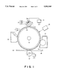
- FIG. 1 is a schematic sectional view showing an ordinary electrophotographic apparatus using the charging member according to the present invention.
- FIG. 2 is a block diagram of a facsimile machine using the electrophotographic apparatus according to the present invention as a printer.
- FIG. 3 is an explanatory view for illustrating a method of measuring a resistance of a surface layer of charging rollers used in Examples.
- FIG. 4 is an explanatory view for illustrating a withstand voltage-measuring apparatus for charging rollers used in Examples.
- a charging member according to the present invention is characterized by a specific surface layer comprising a semiconductive resin as a surface resin and an insulating metal oxide contained in the semiconductive resin.
- the insulating metal oxide may preferably have a volume resistivity of at least 1 ⁇ 10 12 ohm.cm, particularly at least 1 ⁇ 10 13 ohm.cm.
- a volume resistivity of the insulating metal oxide can e measured in the following manner.
- a sample powder i.e., metal oxide particles
- the sample powder is compressed under a pressure of 100 kg/cm 2 (in order to suppress the influence of a resistance of air among particles) by means of a piston disposed within the cylinder.
- a resistance measuring apparatus is electrically connected to an electrode disposed at a bottom part of the cylinder and an electrode disposed at a top part of the piston (i.e., a face opposite to a face being in contact with the sample powder), whereby a resistance between the two electrodes is measured to obtain a volume resistivity of the sample powder.
- the semiconductive resin may preferably have a volume resistivity of 1 ⁇ 10 7 ohm.cm to 1 ⁇ 10 11 ohm.cm, particularly 1 ⁇ 10 8 ohm.cm to 1 ⁇ 10 10 ohm.cm, in view of prevention of leakage and image fogs.
- the volume resistivity of the semiconductive resin can be measured according to a resistance-measuring method (ASTM D-257-6.1.10). More specifically, a 50 ⁇ m-thick resin layer is formed on an aluminum sheet. A voltage of 100 V is applied to the resin-coated sheet under a temperature of 23° C. and a relative humidity of 50%, thus obtaining a volume resistivity of the resin.
- the charging member may preferably have a resistance of 5 ⁇ 10 7 ohm to 5 ⁇ 10 12 ohm, particularly 1 ⁇ 10 8 ohm to 1 ⁇ 10 10 ohm.
- Examples of the insulating metal oxide contained in the semiconductive resin may include: magnesium oxide, zinc oxide, iron oxide, lead oxide, beryllium oxide, cesium oxide, calcium oxide, and zirconium oxide. Among these examples, magnesium oxide may preferably be used.
- the semiconductive resin as a surface resin may include: ionomer (mainly comprising a polymer obtained from ethylene and unsaturated carboxylic acid), polyvinyl alcohol, ethylene-vinyl acetate copolymer, polyurethane elastomer, cellulosic, polyamide, polyvinyl chloride, acrylonitrile-butadiene rubber, chloroprene rubber, acrylic rubber, hydrin rubber, and urethane rubber.
- the semiconductive resin may preferably comprise polyvinyl alcohol, cellulosics, polyamide and hydrin rubber.
- the surface layer of the charging member of the present invention may preferably be prepared by dispersing an insulating metal oxide in a solution of a semiconductive resin in an appropriate solvent to prepare a coating liquid and applying the coating liquid onto an elastic layer by known coating methods such as dipping, spray coating, spinner coating, bead coating, wire bar coating, blade coating, and curtain coating, followed by drying the resultant coating.
- the surface layer may preferably have a thickness of 5-200 ⁇ m.
- THe surface layer may preferably have a maximum height of surface roughness (Rmax) of at least 10 ⁇ m as a lower limit in order to increase a discharge point, thus enhancing a charging efficiency.
- the surface layer may preferably have an Rmax of at most 100 ⁇ m as an upper limit.
- the surface layer may more preferably have an Rmax of 10-50 ⁇ m.
- Rmax can be obtained according to Japan Industrial Standard (JIS) B0601 (reference length of 8 mm).
- the surface layer may preferably comprise 10-150 wt. parts, more preferably 15-100 wt. parts, of the insulating metal oxide on the basis of 100 wt. parts of the semiconductive layer.
- the surface layer may further contain an appropriate amount of an additive such as a colorant or a lubricant.
- the elastic layer of the charging member of the present invention may preferably have a resistance of 1 ⁇ 10 2 ohm to 1 ⁇ 10 5 ohm.
- the elastic layer may generally have a thickness of 1-20 mm.
- the above-mentioned charging member may suitably be applied to various electrophotographic apparatus.
- FIG. 1 is a schematic cross-sectional view of an embodiment of an electrophotographic apparatus including the charging member according to the present invention.
- a drum-type electrophotographic photosensitive member 1 is used as a charge-receiving member or charge-carrying member and comprises an electroconductive support layer 1b such as an aluminum cylinder and a photoconductive layer 1a formed on the support layer 1b.
- the photosensitive member 1 is rotated about an axis 1d at a prescribed peripheral speed in the clockwise direction.
- the photosensitive member 1 is uniformly charged by means of a charging member (i.e., charging roller in this embodiment) 2 for performing primary charging or contact charging to have prescribed polarity and potential at the surface thereof.
- the charging roller 2 comprises a core metal (or a shaft) 2c as an electroconductive support, an elastic layer 2b and a surface layer 2d disposed in this order.
- THe core metal 2c has both end sections at which the core metal is rotatably supported by a bearing member (not shown).
- the core metal 2c is disposed parallel to the axis 1d, and the charging roller 2 is caused to abut upon the photosensitive member 1 under a prescribed pressure exerted by a pressing member (not shown) such as a spring, thus rotating mating with the rotation of the photosensitive member 1.
- the primary charging or contact charging is performed by applying a DC bias voltage or a superposition of a DC bias voltage and an AC bias voltage to the core metal 2c through a friction (or rubbing) electrode 3a by means of a power supply 3, thus providing the peripheral surface of the rotating photosensitive member 1 with a prescribed polarity and a prescribed potential.
- the peripheral surface of the photosensitive member 1 uniformly charged by the charging member 2 as described above is then subjected to imagewise exposure (e.g., laser beam scanning exposure or slit exposure of an original image) by image exposure means 10, whereby an electrostatic latent image corresponding to original image data is formed on the peripheral surface of the photosensitive member 1.
- imagewise exposure e.g., laser beam scanning exposure or slit exposure of an original image
- image exposure means 10 image exposure means 10
- an electrostatic latent image corresponding to original image data is formed on the peripheral surface of the photosensitive member 1.
- the thus formed latent image is developed or visualized by developing means 11 with a toner to form a toner image (or developed image) in sequence.
- the toner image is successively transferred to the front side of a transfer-receiving material 14 such as paper, being timely conveyed from a supply part (not shown) to a transfer position between the photosensitive member 1 and transfer means 12 (i.e., transfer roller in this embodiment) in synchronism with the rotation of the photosensitive member 1, by the transfer means 12.
- the transfer means (roller) 12 is used for charging the back side of the transfer-receiving material 14 so as to have a polarity opposite to that of the toner, whereby the toner image formed no the photosensitive member 1 is transferred to the front side of the material 14.
- the transfer-receiving material 14 having thereon the toner image is detached from the surface of the photosensitive member 1 and is conveyed to fixing means (not shown), thus being subjected to image fixing to be outputted as an image-formed product.
- the transfer-receiving material 14 is carried to reconveying means for conveying the material 14 back to the transfer position.
- the surface of the photosensitive member 1 after the transfer operation is subjected to cleaning by cleaning means 13 for removing and recovering an attached matter, such as a residual toner, from the surface of the photosensitive member 1, thus obtaining a cleaned surface to prepare for the next cycle.
- the charging member 2 may include that in the form of a blade, a block, a rod or a belt in addition to the above-mentioned roller-type charging member as shown in FIG. 1.
- a charging member in the form of a roller or a blade may preferably be used.
- the charging member 2 may be rotated mating with movement of a charge-receiving member in the form of, e.g., a sheet or may be one being not rotatable.
- the charging member 2 may also be rotated for itself at a prescribed peripheral speed in the direction identical to or opposite to the moving direction f the charge-receiving member (e.g., sheet-type) or the rotating direction of the above-mentioned drum-type photosensitive member.
- a plurality of elements or components of an electrophotographic apparatus such as the above-mentioned photosensitive member, charging member developing means and cleaning means may be integrally assembled into a device unit, and the device unit may be attachably and detachably disposed in the apparatus body.
- at least one component selected from a charging member, a charging member, developing means and cleaning means may be integrally assembled together with a photosensitive member into a device unit, and such a device unit is capable of being attached to or detached from the apparatus body by the medium of a guiding means such as rail of the apparatus body.
- a charging member and/or developing means may be used together with a photosensitive member to constitute a device unit.
- image exposure may be effected by using reflection light or transmitted light from an original or by reading a data on the original, converting the data into a signal and then effecting a laser beam scanning, a drive of LEF array or a drive of a liquid crystal shutter array in accordance with the signal.
- FIG. 2 shows such an embodiment by using a block diagram.
- a controller 21 controls an image reader (or image reading unit) 20 and a printer 29.
- the entirety of the controller 21 is regulated by a CPU (central processing unit) 27.
- Read data from the image reader 20 is transmitted through a transmitter circuit 23 to another terminal such as facsimile.
- data received from another terminal is transmitted through a receiver circuit 22 to the printer 29.
- An image memory 26 stores prescribed image data.
- a printer controller 28 controls the printer 29.
- reference numeral 24 denotes a telephone system.
- an image received from a line (or circuit) 25 is demodulated by means of the receiver circuit 22, decoded by the CPU 27, and sequentially stored in the image memory 26.
- image data corresponding to at least one page is stored in the image memory 26, image recording is effected with respect to the corresponding page.
- the CPU 27 reads image data corresponding to one page from the image memory 26, and transmits the decoded data corresponding to one page to the printer controller 28.
- the printer controller 28 controls the printer 29 so that image data recording corresponding to the page is effected.
- the CPU 27 receives another image data corresponding to the next page.
- receiving and recording of an image may be effected by means of the apparatus shown in FIG. 2 in the above-mentioned manner.
- parts means “parts by weight (wt. parts)”.
- the thus prepared rubber roller was subjected to measurement of a resistance as follows.
- FIG. 3 shows a schematic view for illustrating a method of measuring a resistance of an electroconductive rubber roller and a charging roller used herein. More specifically, referring to FIG. 3, an aluminum foil 35 having a width of 10 mm is wound on a rubber roller (or a charging roller) 34. A direct-current (DC) voltage of 250 V is applied between a core metal and the aluminum foil 35, followed by current measurement to obtain a resistance.
- DC direct-current
- the rubber roller showed a resistance of 5 ⁇ 10 4 ohm under an environmental condition of a temperature of 23° C. and a relative humidity of 55%.
- a coating liquid was prepared by Kyowa Kagaku Kogyo K.K.; volume resistivity of 1 ⁇ 10 14 ohm.cm, particle size: 150 ⁇ m-opening sieve passing rate of 100% and 75 ⁇ m-opening sieve passing rate of 99.7%.
- the coating liquid was applied onto the above-prepared rubber roller by dipping and dried at 120° C. for 2 hours to form a 20 ⁇ m-thick surface layer, whereby a charging roller (i.e., a charging member) of the present invention was prepared.
- the semiconductive resin had a maximum surface roughness (Rmax) of 18 ⁇ m.
- the charging roller showed a resistance of 1.5 ⁇ 10 9 ohm under an environmental condition of a temperature of 15° C. and a relative humidity of 10%.
- the thus-prepared charging roller was assembled in a cartridge (EP-L cartridge, mfd. by Canon K.K.) to prepare a device unit.
- the device unit was further assembled in a laser beam printer (Laser SHot A404, mfd. by Canon K.K.) as an electrophotographic apparatus and then subjected to image formation of 3500 sheets (a durability test) under an environmental condition of a temperature 15° C. and a relative humidity of 10%.
- the results are shown in Table 1 appearing hereinbelow.
- the electrophotographic apparatus including the charging roller according to the present invention provided stable image forming properties causing no black spots and black streaks from an initial stage to a stage after 3500 sheets copying, thus ensuring a stable and uniform charging.
- the above-mentioned charging roller was subjected to measurement of a withstand voltage (a withstand voltage test) by using a withstand voltage-measuring apparatus as shown in FIG. 4 in the following manner.
- a charging roller 44 is rotated while being in contact with a metal drum 41.
- the charging roller 44 includes a core metal having both end parts each under a load of 500 gf to be exerted on the metal drum 41.
- the core metal of the charging roller 44 is electrically connected to a high-voltage power supply 47.
- the metal drum is electrically connected to a recorder 50 through the media of a low pass filter 48 and a digital multimeter 49.
- a DC voltage was applied to the above-prepared charging roller from -500 V to -2000 V under an environmental condition of a temperature of 23° C. and a relative humidity of 55%. As a result, no leakage was observed under the voltage application of -2000 V, thus showing a good withstand voltage characteristic.
- a comparative charging roller having a 20 ⁇ m-thick surface layer was prepared in the same manner as in the charging roller mentioned above except that the insulating magnesium oxide (MgO) was omitted from the coating liquid for the surface layer.
- the thus prepared comparative charging roller was evaluated in the same manner as in the charging roller mentioned above according to the present invention. As a result, after 3500 sheets of copying (durability test), black streaks due to charging failure were caused to occur in a resultant sheet.
- a charging roller having a 20 ⁇ m-thick surface layer was prepared in the same manner as in Example 1 except that 100 parts of insulating zinc oxide (ZnO) (Zinc Oxide No. 1, mfd. by Hakusui Kagaku K.K.; volume resistivity of 1 ⁇ 10 15 ohm.cm) was used instead of the MgO used in Example 1.
- ZnO insulating zinc oxide
- the charging roller was evaluated in the same manner as in Example 1. The results are also shown in Table 1 appearing hereinbelow.
- the charging roller of this embodiment provided stable image forming properties (in other words, stable and uniform charging properties) from an initial stage to a stage after 3500 sheets of copying, and also caused no leakage, thus showing a good withstand voltage characteristic.
- a charging roller having a 20 ⁇ m-thick surface layer was prepared in the same manner as in Example 1 except that electroconductive titanium oxide (TiO 2 ) (ET500W, mfd. by Ishihara Sangyo K.K.; volume resistivity of 4 ohm.cm) was used instead of the MgO used in Example 1.
- electroconductive titanium oxide TiO 2
- the charging roller was evaluated in the same manner as in Example 1. The results are shown in Table 1.
- an electrophotographic apparatus including the charging roller provided black spots, thus showing image failure. Further, in a withstand voltage test, leakage was caused to occur (i.e., a leakage current (overcurrent) was observed) at an applied voltage of -700 V, thus showing a poor withstand voltage characteristic.
- a charging roller having a 20 ⁇ m-thick surface layer was prepared in the same manner as in Example 1 except that electroconductive tin oxide (T-1, mfd. by Mitsubishi Material K.K.; volume resistivity of 2 ohm.cm) was used instead of the MgO used in Example 1.
- electroconductive tin oxide T-1, mfd. by Mitsubishi Material K.K.; volume resistivity of 2 ohm.cm
- the charging roller was subjected to measurement of a resistance in the same manner and the same condition as in Example 1 and then subjected to image formation. As a result, a resistance of the charging roller was not uniform in the nip direction, and black streaks due to leakage and black spots due to a dielectric breakdown were caused to occur under an environmental condition of a temperature of 32.5° C. and a relative humidity of 85%.
- a charging roller having a 20 ⁇ m-thick surface layer was prepared in the same manner as in Example 1 except that the stirring time (15 minuets) of the coating liquid for the surface layer was changed to 60 minutes.
- a resultant surface layer had an Rmax of 10 ⁇ m.
- the charging roller was evaluated in the same manner as in Example 1. The results are shown in Table 1.
- a charging roller having a 2 ⁇ m-thick surface layer was prepared in the same manner as in Example 1 except that a coating liquid for a surface layer was prepared through a stirring for 5 minutes by means of a stirrer.
- the surface layer had an Rmax of 100 ⁇ m.
- the charging roller was evaluated in the same manner as in Example 1. The results are shown in Table 1 below.
- a charging roller having a 20 ⁇ m-thick surface layer was prepared in the same manner as in Example 1 except that an aqueous solution of 15 wt. % of polyvinyl alcohol (Gosenol GM-14, mid. by Nippon Gosei Kagaku K.K.; saponification degree of 86.5-89.0 mol. %, polymerization degree of 1000-1500, volume resistivity of 2 ⁇ 10 9 ohm.cm) was used instead of the methoxymethylated nylon solution (solid content of 14 wt. %) used in Example 1.
- polyvinyl alcohol Gosenol GM-14, mid. by Nippon Gosei Kagaku K.K.; saponification degree of 86.5-89.0 mol. %, polymerization degree of 1000-1500, volume resistivity of 2 ⁇ 10 9 ohm.cm
- the charging roller had an Rmax of 25 ⁇ m.
- the charging roller was subjected to measurement of a resistance in the same manner and the same condition as in Example 1 and also subjected to image formation for evaluating image forming properties at an initial stage. As a result, the charging roller showed a uniform resistance (2.5 ⁇ 10 9 ohm.cm) in the nip direction and also provided stable and good images free from black spots and black streaks. When the charging roller was further subjected to a durability test in the same manner as in Example 1, no image failure was caused to occur.
- the charging roller had an Rmax of 29 ⁇ m.
- the charging roller was subjected to measurement of a resistance (3.5 ⁇ 10 10 ohm) in the same manner and the same condition as in Example 1 and also subjected to image formation for evaluating image forming properties at an initial stage. As a result, the charging roller showed a uniform resistance (2.5 ⁇ 10 9 ohm.cm) in the nip direction and also provided stable and good images free from black spots and black streaks. When the charging roller was further subjected to a durability test in the same manner as in Example 1, no image failure was caused to occur.
Landscapes
- Physics & Mathematics (AREA)
- Engineering & Computer Science (AREA)
- Plasma & Fusion (AREA)
- General Physics & Mathematics (AREA)
- Electrostatic Charge, Transfer And Separation In Electrography (AREA)
Priority Applications (1)
| Application Number | Priority Date | Filing Date | Title |
|---|---|---|---|
| US08/405,407 US5502548A (en) | 1992-11-04 | 1995-03-15 | Contact-type charging member which includes an insulating metal oxide in a surface layer thereof |
Applications Claiming Priority (4)
| Application Number | Priority Date | Filing Date | Title |
|---|---|---|---|
| JP4-295136 | 1992-11-04 | ||
| JP29513692 | 1992-11-04 | ||
| US14513393A | 1993-11-03 | 1993-11-03 | |
| US08/405,407 US5502548A (en) | 1992-11-04 | 1995-03-15 | Contact-type charging member which includes an insulating metal oxide in a surface layer thereof |
Related Parent Applications (1)
| Application Number | Title | Priority Date | Filing Date |
|---|---|---|---|
| US14513393A Continuation | 1992-11-04 | 1993-11-03 |
Publications (1)
| Publication Number | Publication Date |
|---|---|
| US5502548A true US5502548A (en) | 1996-03-26 |
Family
ID=17816749
Family Applications (1)
| Application Number | Title | Priority Date | Filing Date |
|---|---|---|---|
| US08/405,407 Expired - Lifetime US5502548A (en) | 1992-11-04 | 1995-03-15 | Contact-type charging member which includes an insulating metal oxide in a surface layer thereof |
Country Status (3)
| Country | Link |
|---|---|
| US (1) | US5502548A (fr) |
| EP (1) | EP0596477B1 (fr) |
| DE (1) | DE69316828T2 (fr) |
Cited By (5)
| Publication number | Priority date | Publication date | Assignee | Title |
|---|---|---|---|---|
| US5761581A (en) * | 1995-05-30 | 1998-06-02 | Ricoh Company, Ltd. | Image forming apparatus charging member formed of sequential overlying layers of elastic material |
| US5822675A (en) * | 1996-02-13 | 1998-10-13 | Dow Corning S.A. | Heating elements and a process for their manufacture |
| US6317574B1 (en) * | 1999-02-25 | 2001-11-13 | Canon Kabushiki Kaisha | Charging member, process cartridge, and image forming apparatus |
| EP1355200A1 (fr) * | 2002-04-17 | 2003-10-22 | Canon Kabushiki Kaisha | Dispositif de chargement par contact utilisant des particules chargés et appareil de formation d'images l'utilisant |
| CN100392525C (zh) * | 2001-02-02 | 2008-06-04 | 富士施乐株式会社 | 充电装置以及使用充电装置的成像装置 |
Families Citing this family (5)
| Publication number | Priority date | Publication date | Assignee | Title |
|---|---|---|---|---|
| JP3236224B2 (ja) * | 1995-09-08 | 2001-12-10 | キヤノン株式会社 | 画像形成装置 |
| US6141516A (en) * | 1996-06-28 | 2000-10-31 | Xerox Corporation | Fluorinated carbon filled fluoroelastomer outer layer |
| JP4105830B2 (ja) * | 1999-07-19 | 2008-06-25 | 株式会社リコー | 帯電装置における帯電ローラの各層の抵抗率決定方法 |
| US6620476B2 (en) | 1999-08-13 | 2003-09-16 | Xerox Corporation | Nonbleeding fluorinated carbon and zinc oxide filled layer for bias charging member |
| US6203855B1 (en) | 1999-08-13 | 2001-03-20 | Xerox Corporation | Process for preparing nonbleeding fluorinated carbon and zinc oxide filler layer for bias charging member |
Citations (5)
| Publication number | Priority date | Publication date | Assignee | Title |
|---|---|---|---|---|
| US4371252A (en) * | 1980-03-10 | 1983-02-01 | Tokyo Shibaura Denki Kabushiki Kaisha | Contact type charging device with pliable contact member |
| EP0308185A2 (fr) * | 1987-09-14 | 1989-03-22 | Canon Kabushiki Kaisha | Dispositif de charge |
| EP0329366A1 (fr) * | 1988-02-19 | 1989-08-23 | Canon Kabushiki Kaisha | Elément pour charger |
| US5112708A (en) * | 1988-02-11 | 1992-05-12 | Canon Kabushiki Kaisha | Member for charging with surface layer of n-alkoxymethylated nylon effecting charging at lower voltage |
| EP0534437A2 (fr) * | 1991-09-27 | 1993-03-31 | Bridgestone Corporation | Appareil et méthode de chargement par contact |
-
1993
- 1993-11-03 DE DE69316828T patent/DE69316828T2/de not_active Expired - Lifetime
- 1993-11-03 EP EP93117827A patent/EP0596477B1/fr not_active Expired - Lifetime
-
1995
- 1995-03-15 US US08/405,407 patent/US5502548A/en not_active Expired - Lifetime
Patent Citations (5)
| Publication number | Priority date | Publication date | Assignee | Title |
|---|---|---|---|---|
| US4371252A (en) * | 1980-03-10 | 1983-02-01 | Tokyo Shibaura Denki Kabushiki Kaisha | Contact type charging device with pliable contact member |
| EP0308185A2 (fr) * | 1987-09-14 | 1989-03-22 | Canon Kabushiki Kaisha | Dispositif de charge |
| US5112708A (en) * | 1988-02-11 | 1992-05-12 | Canon Kabushiki Kaisha | Member for charging with surface layer of n-alkoxymethylated nylon effecting charging at lower voltage |
| EP0329366A1 (fr) * | 1988-02-19 | 1989-08-23 | Canon Kabushiki Kaisha | Elément pour charger |
| EP0534437A2 (fr) * | 1991-09-27 | 1993-03-31 | Bridgestone Corporation | Appareil et méthode de chargement par contact |
Cited By (6)
| Publication number | Priority date | Publication date | Assignee | Title |
|---|---|---|---|---|
| US5761581A (en) * | 1995-05-30 | 1998-06-02 | Ricoh Company, Ltd. | Image forming apparatus charging member formed of sequential overlying layers of elastic material |
| US5822675A (en) * | 1996-02-13 | 1998-10-13 | Dow Corning S.A. | Heating elements and a process for their manufacture |
| US6317574B1 (en) * | 1999-02-25 | 2001-11-13 | Canon Kabushiki Kaisha | Charging member, process cartridge, and image forming apparatus |
| CN100392525C (zh) * | 2001-02-02 | 2008-06-04 | 富士施乐株式会社 | 充电装置以及使用充电装置的成像装置 |
| EP1355200A1 (fr) * | 2002-04-17 | 2003-10-22 | Canon Kabushiki Kaisha | Dispositif de chargement par contact utilisant des particules chargés et appareil de formation d'images l'utilisant |
| US6847796B2 (en) | 2002-04-17 | 2005-01-25 | Canon Kabushiki Kaisha | Charging member and image forming apparatus provided with the same |
Also Published As
| Publication number | Publication date |
|---|---|
| DE69316828D1 (de) | 1998-03-12 |
| DE69316828T2 (de) | 1998-06-25 |
| EP0596477B1 (fr) | 1998-02-04 |
| EP0596477A3 (fr) | 1995-03-08 |
| EP0596477A2 (fr) | 1994-05-11 |
Similar Documents
| Publication | Publication Date | Title |
|---|---|---|
| KR0158921B1 (ko) | 전자 사진용 감광성 부재, 이를 사용한 전자 사진 장치 및 장치 유닛 | |
| US5235386A (en) | Charging device having charging member, process cartridge and image forming apparatus | |
| JP2584873B2 (ja) | 電子写真装置 | |
| US5502548A (en) | Contact-type charging member which includes an insulating metal oxide in a surface layer thereof | |
| EP0747780B1 (fr) | Appareil de formation d'images comprenant un membre de chargement par contact | |
| JP3126889B2 (ja) | 電子写真感光体、該電子写真感光体を有するプロセスカ−トリッジ及び電子写真装置 | |
| US5418605A (en) | Charging device and image forming apparatus | |
| JP2897494B2 (ja) | プロセスカートリッジ | |
| JPH07209959A (ja) | 帯電装置 | |
| US20140037337A1 (en) | Bias charge roller and apparatus incorporating the bias charge roller | |
| JP3184026B2 (ja) | 帯電部材及び電子写真装置 | |
| US5881343A (en) | Charging method and charging device | |
| US6001454A (en) | Charging member and electrophotographic apparatus using the same | |
| JP2952140B2 (ja) | 帯電部材およびそれを用いた装置 | |
| JP3204858B2 (ja) | 接触帯電部材及びこれを用いる帯電装置 | |
| JP3284626B2 (ja) | 帯電部材 | |
| JP3656473B2 (ja) | 画像形成装置及び画像形成方法 | |
| JP2921716B2 (ja) | 帯電用部材 | |
| JPH06295085A (ja) | 電子写真感光体、該電子写真感光体を有する電子写真装置および装置ユニット | |
| US5860046A (en) | Charging method and charging device | |
| JP2929558B2 (ja) | 帯電用部材 | |
| JP2921715B2 (ja) | 帯電用部材 | |
| JP3227230B2 (ja) | 電子写真装置 | |
| US5637391A (en) | Powder coated charge roller | |
| JP2024013572A (ja) | 画像形成装置およびそれを用いる画像形成方法、帯電装置 |
Legal Events
| Date | Code | Title | Description |
|---|---|---|---|
| STCF | Information on status: patent grant |
Free format text: PATENTED CASE |
|
| CC | Certificate of correction | ||
| FPAY | Fee payment |
Year of fee payment: 4 |
|
| FEPP | Fee payment procedure |
Free format text: PAYOR NUMBER ASSIGNED (ORIGINAL EVENT CODE: ASPN); ENTITY STATUS OF PATENT OWNER: LARGE ENTITY Free format text: PAYER NUMBER DE-ASSIGNED (ORIGINAL EVENT CODE: RMPN); ENTITY STATUS OF PATENT OWNER: LARGE ENTITY |
|
| FPAY | Fee payment |
Year of fee payment: 8 |
|
| FPAY | Fee payment |
Year of fee payment: 12 |