US5633788A - Power converter control system - Google Patents
Power converter control system Download PDFInfo
- Publication number
- US5633788A US5633788A US08/648,396 US64839696A US5633788A US 5633788 A US5633788 A US 5633788A US 64839696 A US64839696 A US 64839696A US 5633788 A US5633788 A US 5633788A
- Authority
- US
- United States
- Prior art keywords
- command value
- signal
- voltage command
- corrected
- generating
- Prior art date
- Legal status (The legal status is an assumption and is not a legal conclusion. Google has not performed a legal analysis and makes no representation as to the accuracy of the status listed.)
- Expired - Fee Related
Links
- 230000003111 delayed effect Effects 0.000 claims description 6
- 230000006870 function Effects 0.000 claims description 5
- 238000010586 diagram Methods 0.000 description 12
- 101100023550 Mycobacterium bovis (strain ATCC BAA-935 / AF2122/97) cmaD gene Proteins 0.000 description 7
- 101150024128 mmaA1 gene Proteins 0.000 description 7
- 101100077240 Mycobacterium tuberculosis (strain ATCC 25177 / H37Ra) mmaA3 gene Proteins 0.000 description 6
- 101100077241 Mycobacterium tuberculosis (strain ATCC 25618 / H37Rv) mmaA3 gene Proteins 0.000 description 6
- 239000000203 mixture Substances 0.000 description 6
- 101150084640 mmaA2 gene Proteins 0.000 description 6
- 230000009467 reduction Effects 0.000 description 6
- 101150110971 CIN7 gene Proteins 0.000 description 4
- 101100286980 Daucus carota INV2 gene Proteins 0.000 description 4
- 101150110298 INV1 gene Proteins 0.000 description 4
- 101100397044 Xenopus laevis invs-a gene Proteins 0.000 description 4
- 101100397045 Xenopus laevis invs-b gene Proteins 0.000 description 4
- 230000007423 decrease Effects 0.000 description 3
- 238000001514 detection method Methods 0.000 description 2
- 230000000694 effects Effects 0.000 description 2
- 230000008030 elimination Effects 0.000 description 2
- 238000003379 elimination reaction Methods 0.000 description 2
- 238000000034 method Methods 0.000 description 2
- 230000004044 response Effects 0.000 description 2
- ATJFFYVFTNAWJD-UHFFFAOYSA-N Tin Chemical compound [Sn] ATJFFYVFTNAWJD-UHFFFAOYSA-N 0.000 description 1
- 102100029469 WD repeat and HMG-box DNA-binding protein 1 Human genes 0.000 description 1
- 101710097421 WD repeat and HMG-box DNA-binding protein 1 Proteins 0.000 description 1
- 238000013459 approach Methods 0.000 description 1
- 239000003990 capacitor Substances 0.000 description 1
- 230000008859 change Effects 0.000 description 1
- 238000006243 chemical reaction Methods 0.000 description 1
- 238000012986 modification Methods 0.000 description 1
- 230000004048 modification Effects 0.000 description 1
- 230000008569 process Effects 0.000 description 1
Images




Classifications
-
- H—ELECTRICITY
- H02—GENERATION; CONVERSION OR DISTRIBUTION OF ELECTRIC POWER
- H02M—APPARATUS FOR CONVERSION BETWEEN AC AND AC, BETWEEN AC AND DC, OR BETWEEN DC AND DC, AND FOR USE WITH MAINS OR SIMILAR POWER SUPPLY SYSTEMS; CONVERSION OF DC OR AC INPUT POWER INTO SURGE OUTPUT POWER; CONTROL OR REGULATION THEREOF
- H02M7/00—Conversion of AC power input into DC power output; Conversion of DC power input into AC power output
- H02M7/42—Conversion of DC power input into AC power output without possibility of reversal
- H02M7/44—Conversion of DC power input into AC power output without possibility of reversal by static converters
- H02M7/48—Conversion of DC power input into AC power output without possibility of reversal by static converters using discharge tubes with control electrode or semiconductor devices with control electrode
- H02M7/505—Conversion of DC power input into AC power output without possibility of reversal by static converters using discharge tubes with control electrode or semiconductor devices with control electrode using devices of a thyratron or thyristor type requiring extinguishing means
- H02M7/515—Conversion of DC power input into AC power output without possibility of reversal by static converters using discharge tubes with control electrode or semiconductor devices with control electrode using devices of a thyratron or thyristor type requiring extinguishing means using semiconductor devices only
- H02M7/525—Conversion of DC power input into AC power output without possibility of reversal by static converters using discharge tubes with control electrode or semiconductor devices with control electrode using devices of a thyratron or thyristor type requiring extinguishing means using semiconductor devices only with automatic control of output waveform or frequency
-
- H—ELECTRICITY
- H02—GENERATION; CONVERSION OR DISTRIBUTION OF ELECTRIC POWER
- H02M—APPARATUS FOR CONVERSION BETWEEN AC AND AC, BETWEEN AC AND DC, OR BETWEEN DC AND DC, AND FOR USE WITH MAINS OR SIMILAR POWER SUPPLY SYSTEMS; CONVERSION OF DC OR AC INPUT POWER INTO SURGE OUTPUT POWER; CONTROL OR REGULATION THEREOF
- H02M7/00—Conversion of AC power input into DC power output; Conversion of DC power input into AC power output
- H02M7/42—Conversion of DC power input into AC power output without possibility of reversal
- H02M7/44—Conversion of DC power input into AC power output without possibility of reversal by static converters
- H02M7/48—Conversion of DC power input into AC power output without possibility of reversal by static converters using discharge tubes with control electrode or semiconductor devices with control electrode
- H02M7/53—Conversion of DC power input into AC power output without possibility of reversal by static converters using discharge tubes with control electrode or semiconductor devices with control electrode using devices of a triode or transistor type requiring continuous application of a control signal
- H02M7/537—Conversion of DC power input into AC power output without possibility of reversal by static converters using discharge tubes with control electrode or semiconductor devices with control electrode using devices of a triode or transistor type requiring continuous application of a control signal using semiconductor devices only, e.g. single switched pulse inverters
- H02M7/538—Conversion of DC power input into AC power output without possibility of reversal by static converters using discharge tubes with control electrode or semiconductor devices with control electrode using devices of a triode or transistor type requiring continuous application of a control signal using semiconductor devices only, e.g. single switched pulse inverters in a push-pull configuration
- H02M7/53803—Conversion of DC power input into AC power output without possibility of reversal by static converters using discharge tubes with control electrode or semiconductor devices with control electrode using devices of a triode or transistor type requiring continuous application of a control signal using semiconductor devices only, e.g. single switched pulse inverters in a push-pull configuration with automatic control of output voltage or current
-
- H—ELECTRICITY
- H02—GENERATION; CONVERSION OR DISTRIBUTION OF ELECTRIC POWER
- H02M—APPARATUS FOR CONVERSION BETWEEN AC AND AC, BETWEEN AC AND DC, OR BETWEEN DC AND DC, AND FOR USE WITH MAINS OR SIMILAR POWER SUPPLY SYSTEMS; CONVERSION OF DC OR AC INPUT POWER INTO SURGE OUTPUT POWER; CONTROL OR REGULATION THEREOF
- H02M7/00—Conversion of AC power input into DC power output; Conversion of DC power input into AC power output
- H02M7/42—Conversion of DC power input into AC power output without possibility of reversal
- H02M7/44—Conversion of DC power input into AC power output without possibility of reversal by static converters
- H02M7/48—Conversion of DC power input into AC power output without possibility of reversal by static converters using discharge tubes with control electrode or semiconductor devices with control electrode
-
- H—ELECTRICITY
- H02—GENERATION; CONVERSION OR DISTRIBUTION OF ELECTRIC POWER
- H02M—APPARATUS FOR CONVERSION BETWEEN AC AND AC, BETWEEN AC AND DC, OR BETWEEN DC AND DC, AND FOR USE WITH MAINS OR SIMILAR POWER SUPPLY SYSTEMS; CONVERSION OF DC OR AC INPUT POWER INTO SURGE OUTPUT POWER; CONTROL OR REGULATION THEREOF
- H02M7/00—Conversion of AC power input into DC power output; Conversion of DC power input into AC power output
- H02M7/42—Conversion of DC power input into AC power output without possibility of reversal
- H02M7/44—Conversion of DC power input into AC power output without possibility of reversal by static converters
- H02M7/48—Conversion of DC power input into AC power output without possibility of reversal by static converters using discharge tubes with control electrode or semiconductor devices with control electrode
- H02M7/505—Conversion of DC power input into AC power output without possibility of reversal by static converters using discharge tubes with control electrode or semiconductor devices with control electrode using devices of a thyratron or thyristor type requiring extinguishing means
- H02M7/515—Conversion of DC power input into AC power output without possibility of reversal by static converters using discharge tubes with control electrode or semiconductor devices with control electrode using devices of a thyratron or thyristor type requiring extinguishing means using semiconductor devices only
- H02M7/525—Conversion of DC power input into AC power output without possibility of reversal by static converters using discharge tubes with control electrode or semiconductor devices with control electrode using devices of a thyratron or thyristor type requiring extinguishing means using semiconductor devices only with automatic control of output waveform or frequency
- H02M7/527—Conversion of DC power input into AC power output without possibility of reversal by static converters using discharge tubes with control electrode or semiconductor devices with control electrode using devices of a thyratron or thyristor type requiring extinguishing means using semiconductor devices only with automatic control of output waveform or frequency by pulse width modulation
Definitions
- This invention relates to a power converter control system, and more particularly to a control system for pulse-width modulation-controlled (PWM control) converters which convert AC power to DC power and PWM control inverters which convert DC power to AC power.
- PWM control pulse-width modulation-controlled
- FIG. 13 shows a schematic diagram of one phase (the U phase) of a prior art PWM control inverter.
- FIG. 13(a) shows the main circuit of a power converter.
- V d1 , V d2 are DC voltage sources
- S 1 , S 2 are self-turn-off devices
- D 1 , D 2 are free-wheeling diodes
- LOAD is a load
- CT u is a current detector.
- FIG. 13(b) shows the control circuit for the power converter.
- C u , C 1 are comparators
- G u (S) is a current control compensation circuit
- PWMC is a pulse-width modulation control circuit
- TRG is a carrier wave generator
- SM is a Schmitt circuit
- GC is a gate circuit.
- load current I u is detected by current detector CT u .
- carrier wave generator TRG In pulse-width modulation control circuit PWMC, carrier wave generator TRG generates a triangular wave X. This is compared with inputted signal e u by comparator C 1 , and a gate signal g u is produced via Schmitt circuit SM. Gate circuit GC inputs this gate signal g u and produces gate signals g 1 and g 2 and for self-turn-off devices S 1 and S 2 . The composition of this circuit explained later.
- voltage command value e u and its related values K MAX , X, E a and E b use normalized values.
- FIG. 14 is a time chart to illustrate the operation of PWM control circuit PWMC in FIG. 13. That is to say,
- V u +V d /2, when S 1 is ON (S 2 is OFF):
- V u -V d /2, when S 1 is OFF (S 2 is ON).
- the mean value MV u of inverter output voltage V u (shown by the pecked line) becomes a value proportional to input signal e u . Therefore, this input signal e u becomes the inverter voltage command value.
- PWM control inverters can obtain output voltage V u proportional to voltage command value e u . They are therefore widely used in the driving systems of AC motors as variable voltage variable frequency power sources.
- GTO gate turn-off thyristors
- devices well-known, snubbey circuits are connected in parallel to the devices.
- the device is temporarily switched ON in order to initialize (discharge) the capacitor of this snubber circuit, a constant-time ON state must be maintained for the device.
- minimum ON, OFF times are determined by the characteristic of the device itself, and the pulse-width of the gate signal is supplied to satisfy this.
- +k MAX and -k MAX express an upper limit value and a lower limit value of voltage command value e u .
- Output voltage V u which is proportional to this voltage command value e u within the limits +k MAX ⁇ e u ⁇ -k MAX can be generated.
- the voltage command value e u is controlled to be within the limits of +k MAX ⁇ e u ⁇ -k MAX by providing a limiter circuit or the like (not illustrated).
- one object of this invention is to provide a power converter control system which executes control so that an output voltage proportional to the input signal can be generated, while ensuring the minimum ON time or the minimum OFF time of the device, and thus can increase the utilization factor of the converter, even when the absolute value of that input signal(the voltage command value) is great,
- Another object of this invention is to provide a power converter control system which can reduce the voltage of the DC power source and in which reduction in size of the power converter, increased efficiency and cost reduction can be achieved.
- the control system includes a voltage command value generator for the power converter, a carrier wave generator and a circuit for correcting at least one of the voltage command value and the frequency of the carrier wave to generate as a corrected voltage command value and a corrected carrier wave.
- the control system further includes a gate pulse signal generator for receiving a first signal and a second signal and for comparing the first and second signals to generate gate pulse signals to the self-turn-off devices fop controlling the power converter based on a comparison result.
- the voltage command value is taken as e (-1 ⁇ e ⁇ +1), and a level setting value is taken as E a (0 ⁇ E a ⁇ 1).
- the gate pulse signal generator receives the voltage command value and the carrier wave as the first and second signals when -E a ⁇ e ⁇ +E a .
- the gate pulse signal generator receives one of the voltage command value and the corrected voltage command value as the first signal and one of the carrier wave and the corrected carrier wave as the second signal when e ⁇ -E a or +E a ⁇ e.
- a control system for a pulse-width modulation controlled power converter composed of self-turn-off devices.
- the control system includes a voltage command value generator for the power converter, a carrier wave generator and a circuit for correcting the frequency of the carrier wave to generate as a corrected carrier wave.
- the control system further includes a gate pulse signal generator for receiving a first signal and s second signal and for comparing the first and second signals to generate gate pulse signals to the self-turn-off devices for controlling the power converter based on a comparison result.
- the voltage command value is taken ss e (-1 ⁇ e ⁇ +1), and a level setting value is taken as E a (0 ⁇ E a ⁇ 1).
- the gate pulse signal generator receives the voltage command value and the carrier wave as the first and second signals when -E a ⁇ e ⁇ +E a .
- the gate pulse signal generator receives the voltage command value as the first signal and the corrected carrier wave as the second signal when e ⁇ -E a or +E a ⁇ e.
- a control system for a pulse-width modulation controlled power converter composed of self-turn-off devices.
- the control system includes a voltage command value generator for the power converter, a carrier wave generator and a circuit for correcting the voltage command value to generate as a corrected voltage command value.
- the control system further includes a gate pulse signal generator for receiving a first signal and a second signal and for comparing the first and second signals to generate gate pulse signals to the self-turn-off devices for controlling the power converter based on a comparison result.
- the voltage command value is taken as e (-1 ⁇ e ⁇ +1), and a level setting value is taken as E a (0 ⁇ E ⁇ 1).
- the gate pulse signal generator receives the voltage command value and the carrier wave as the first and second signals when -E a ⁇ e ⁇ +E a .
- the gate pulse signal generator receives the corrected voltage command value as the first signal and the carrier wave as the second signal when e ⁇ -E a or +E a ⁇ e.
- the control system includes a voltage command value generator for the power converter, a carrier wave generator and a gate pulse signal generator for receiving the voltage command value and the carrier wave and for comparing the voltage command value and the carrier wave to generate gate pulse signals based on a comparison result.
- the control system further includes a correction circuit connected to receive the voltage command value and the gate pulse signals for generating corrected gate pulse signals to the self-turn-off devices for controlling the power converter.
- the voltage command value is taken as e (-1 ⁇ e ⁇ +1), and a level setting value is taken as E a (0 ⁇ E a ⁇ 1).
- the correction circuit generates the gate pulse signals as the corrected gate pulse signals as they stand, when -E a ⁇ e ⁇ +Ea.
- the correction circuit corrects a pulse-width (ti) of the gate pulse signals when e ⁇ -E a or +E a ⁇ e, and generates gate pulse signals with a corrected pulse-width (ti') as the corrected gate pulse signals only when the corrected pulse-width (ti') is equal to or larger than a set time (ts).
- voltage command value e (-1 ⁇ e ⁇ +1) is supplied from the circuit which controls the output current of the power converter.
- the output voltage of the power converter is controlled by normal pulse-width modulation control when -k MAX ⁇ e ⁇ +k MAX .
- the output voltage of the power converter is controlled by adjusting the pulse interval of the pulse with the constant width ⁇ t which satisfies the minimum ON time (or minimum OFF time) of the device.
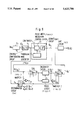
- FIG. 1 is a schematic diagram of the main circuit and the control circuit showing an embodiment of a power converter control system of this invention
- FIG. 2 is a characteristic graph to illustrate the operation of the control system in FIG. 1;
- FIG. 3 is a time chart to illustrate the operation of the system in FIG. 1;
- FIG. 4 is a block diagram of the gate circuit GC of the system in FIG. 1;
- FIG. 5 is a time chart to illustrate the operation of the gate circuit GC in FIG. 4;
- FIG. 6 is a schematic diagram of the main circuit and the control circuit showing another embodiment of a power converter control system of this invention.
- FIG. 7 is a characteristic graph to illustrate the control operation of the system in FIG. 6;
- FIG. 8 is a time chart to illustrate the control operation in FIG. 6;
- FIG. 9 is a control block diagram showing a further embodiment of the power converter control system of this invention.
- FIG. 10 is a flow-chart to illustrate the operating process of FIG. 9;
- FIG. 11 is a diagram to illustrate PWM control operation in FIG. 9 when the voltage command value is positive;
- FIG. 12 is a diagram to illustrate PWM control operation in FIG. 9 when the voltage command value is negative;
- FIG. 13 is a schematic diagram of the main circuit and the control circuit to illustrate a prior art power converter control system
- FIG. 14 is a time chart to illustrate the prior art control system in FIG. 13.
- FIG. 1 shows an embodiment of a power converter control system of this invention.
- FIG. 1(a) is a schematic diagram of the main circuit
- FIG. 1(b) is a block diagram of the control circuit.
- V d1 , V d2 are DC voltage sources
- S 1 , S 2 are self-turn-off devices
- D 1 , D 2 are free-wheeling diodes
- LOAD is load
- CT u is current detector.
- the composition of this main circuit is the same as that in FIG. 13(a).
- comparator C u current control compensation circuit G u (S)
- FX function generator
- V/f voltage/frequency converter
- TRG triangular wave generator
- PWM control circuit pulse-width modulation control circuit
- PWMCA pulse-width modulation control circuit
- U-phase load current I u is detected by current detector CT u , and is inputted to comparator C u of the current control circuit.
- This deviation ⁇ u is amplified by the following control compensation circuit G u (S) to Generate voltage command value e u .
- This voltage command value e u is inputted to PWM control circuit PWMCA and, at the same time, is inputted to function generator FX.
- Output signal e 0 of function generator FX is inputted to the following voltage/frequency converter V/f, and is converted by voltage/frequency conversion to a clock signal of frequency f CL proportional to e 0 .
- This clock signal is inputted to the following triangular wave generator TRG and determines the carrier wave frequency f c of PWM control.
- ⁇ E a , and becomes f c f c0 ⁇ (1-
- ⁇ k MAX , and becomes f c f c0 ⁇ (1-
- FIG. 3 shows an example of the PWM control operation of the system in FIG. 1.
- e u is voltage command value
- X is carrier wave (triangular wave) signal
- +k MAX and -k MAX shown by the pecked lines are the maximum modulation factors of prior art PWM control
- g u is the signal
- end V u is inverter output voltage.
- V u +V d /2, when S 1 is ON (S 2 is OFF);
- V u -V d /2, when S 2 is ON (S 1 is OFF).
- Mean value MV u of inverter output voltage V u becomes a value proportional to voltage command value e u .
- the "1" and "0" periods of gate signal g u always becomes longer than the minimum ON time (or minimum OFF time) ⁇ t of devices S 1 and S 2 which compose the inverter. Thus there is no problem of any kind.
- PWM control carrier wave frequency f c f c0 ⁇ (1-e u )/(1-k MAX ).
- mean value MV of inverter output voltage V u becomes a value proportional to voltage command value e u in the same way as in normal PWM control.
- mean value MV u of inverter output voltage V u can be obtained as a value proportional to voltage command value e u even in the region of e u >+k MAX . Also, the minimum ON time (minimum OFF time) ⁇ t of devices S 1 and S 2 which compose the inverter can be satisfied.
- mean value MV u of inverter output voltage V u becomes a value proportional to voltage command value e u .
- the period ⁇ t of gate signal g u 1 becomes constant, and the minimum ON time (minimum OFF time) of devices S 1 and S 2 which compose the inverter can be satisfied.
- gate signal g u should be processed by gate circuit GC so that the minimum ON time (or minimum OFF time) of the devices are satisfied whatever the case may be.
- FIG. 4 shows gate circuit GC of the system in FIG. 1.
- IN is an inversion circuit
- MMA1 to MMA3 and MMB1 to MMB3 are monomulti circuits
- AND1 and AND2 are AND circuits
- OR1 and OR2 are OR circuits.
- FIG. 5 shows a time chart to illustrate the operation of FIG. 4.
- g u is a gate signal
- Ig u is an inversion signal of gate signal g u obtained via inversion circuit IN;
- m 1a is an output signal of monomulti MMA1 which operates at the falling of gate signal g u ;
- m 2a is an output signal of monomulti MMA2 which operates at the falling of gate signal g u ;
- m 3a is an output signal of monomulti MMA3 which operates at the falling of output signal m 2a ;
- m 1b is an output signal of monomulti MMB1 which operates at the falling of inversion signal Ig u ;
- m 2b is an output signal of monomulti MMB2 which operates at the falling of inversion signal Ig u ;
- m 3b is an output signal of monomulti MMB3 which operates at the falling of output signal m 2b ;
- g 1 and g 2 are gate signals of devices S 1 and S 2 .
- Gate signals g 1 and g 2 are obtained by executing the following logic operations following the circuit in FIG. 4.
- Im 2a is taken as an inversion value of signal m 2a
- Im 2b is an inversion value of signal m 2b .
- Monomulti circuits MMA1 and MMA2 operate when signal g u shifts from “1" to “0". However, when signal m 1b is 0, it provides an interlock so that they do not operate. Similarly, monomulti circuits MMB1 and MMB2 operate when inversion signal Ig u shifts from "1" to "0". However, when signal m 1a is 0, it provides an interlock so that they do not operate.
- Gate signal g 1 of device S 1 is obtained by the logic operation described above, and becomes "0" only during time t OFF from the point of the falling of gate signal g u ', and this satisfies the minimum OFF time of device S 1 . Also, gate signal g 2 of device S 2 becomes "1" delayed only by time t D from the point of the falling of signal g u , and device S 2 is caused to be ON only duping time t ON . Therefore, this satisfies the minimum ON time of device S 2 .
- gate signal g 2 of device S 2 becomes "0" only during the time t OFF from the point of the falling of inversion signal Ig u , and this satisfies the minimum OFF time of device S 2 .
- gate signal g 1 of device S 1 becomes "1" delayed only by time t D from the point of the falling of inversion signal Ig u , and device S 1 is caused to be ON only during time t ON . Therefore, this satisfies the minimum ON time of device S 1 .
- output voltage V u of inverter proportional to voltage command value e u can be continuously obtained even in the region where the absolute value of voltage command value e u is greater than the maximum modulation factor k MAX of the PWM control. Also, it is possible to satisfy the minimum ON time or minimum OFF time of the devices which compose the converter. As a result, when exercising PWM control of power converters such as inverters or converters, the utilization factor of the converter can be greatly increased. Thus, reduction in the voltage V d of the DC power becomes possible. Therefore reduction in size of the converter, increased efficiency and cost-reduction can be achieved.
- FIG. 6 shows another embodiment of the power converter control system of this invention.
- FIG. 6(a) is a schematic diagram of the main circuit
- FIG. 6(b) is a block diagram of its control circuit.
- V d1 , V d2 are DC voltage sources
- S 1 , S 2 are self-turn-off devices
- D 1 , D 2 are free-wheeling diodes
- LOAD load
- CT u current detector.
- the composition of this main circuit is the same as that in FIG. 1(a). However, the composition of the control circuit in FIG. 6(b) differs. That is to say the control circuit shown in FIG.
- 6(b) is composed of comparator C u , current control compensation circuit G u (S), an adder A 1 , a subtractor A 2 , sample hold circuits SH 1 , SH 2 , a signal correction circuit SX, pulse-width modulation control circuit (PWM control circuit) PWMC and gate circuit GC.
- This drawing shows only the portion for one phase (e.g. the U phase). In the case of a 3-phase load, the portions for the other two phases (V and W phases) are composed in the same way.
- U-phase load current I u is detected by current detector CT u , and is inputted to comparator C u of the current control circuit.
- This deviation ⁇ u is amplified by the following control compensation circuit G u (S) to generate an original voltage command value e u .
- This original voltage command value e u is inputted to adder A 1 and added to an error signal ⁇ e which is held by second sample hold circuit SH 2 .
- Output signal e 1 of that sample hold circuit SH 1 is inputted to the following signal correction circuit SX, and is converted to a new voltage command value e 2 depending on its size.
- FIG. 7 shows a practical example of the input/output characteristics of signal correction circuit SX.
- the input is output signal e 1 from sample hold circuit SH 1 .
- New voltage command value e 2 is outputted by comparing signal e 1 and level setting values E a and E b (0 ⁇ E a ⁇ E b ⁇ 1) such that
- This voltage command value e 2 is inputted to PWM control circuit PWMC in FIG. 6.
- Gate circuit GC receives output gate signal g u of PWM control circuit PWMC, and outputs gate signals g 1 and g 2 for self-turn-off devices S 1 and S 2 .
- the circuit compositions of PWM control circuit PWMC and gate circuit GC are respectively the same as those in FIG. 13(b) and FIG. 4.
- level setting value E a is set equal to the maximum modulation factor K MAX OF PWM control.
- Second sample hold circuit SH 2 operates in synchronization with PWM control carrier wave signal X from PWM control circuit PWMC, however it operates by shifting its timing slightly from the operation of first sample hold circuit SH 1 .
- e u shows original voltage command value
- X is PWM control carrier wave signal
- e 2 is new PWM control input signal
- SP 1 and SP 2 are timing signals for sample hold circuits SH 1 and SH 2 when e u >0
- SP 1 ' and SP 2 ' are timing signals for sample hold circuits SH 1 and SH 2 when e u >0
- g u is gate signal
- V u is inverter output voltage
- sample hold circuits SH 1 and SH 2 operate with timing signals SP 1 and SP 2 .
- first sample hold circuit SH 1 is operated in synchronization with PWM control carrier wave signal (carrier signal) X, and takes in the sum of original voltage command value e u and error signal ⁇ e held in second sample hold circuit SH 2 .
- sample hold circuit SH 1 When original voltage command value e u has become e u ⁇ -E a , sample hold circuit SH 1 operates by timing signal SP 1 ' at times t 0 ', t 1 ', t 2 '. Sample hold circuit SH 2 operates by timing signal SP 2 ' at times delayed by time t d , respectively.
- Carrier wave frequency f c of PWM control circuit PWMC in the embodiment in FIG. 6 differs from that in the embodiment in FIG. 1, and is constant.
- FIG. 9 shows part, that is to say the U-phase only, of the power converter control system of the PWM control of this invention.
- SW1 and SW2 are switches which operate in response to the output signals of discrimination circuit Ga;
- CAL is a calculation circuit which has a memory which stores an error time ⁇ ti when a pulse width ti of a control pulse Pi is narrower than a set time ts, as described later;
- TCONT is a pulse circuit which outputs pulse Ps of a width of set time ts.
- INV1 and INV2 are inversion circuits.
- control pulse Pi(g u ) which is obtained by the comparison of voltage command value e u and triangular wave X from carrier wave generator TRG, is inputted to a terminal b of switch SW1 and to inversion circuit INV1. Voltage command value e u is inputted to discrimination circuit Ga. Also, an output signal IPi of inversion circuit INV1 is inputted to a terminal c of switch SW1, and output signal Sk of discrimination circuit Ga is inputted to switches SW1 and SW2.
- Pulse circuit TCONT outputs pulse Ps in synchronization with input pulse Pi to calculation circuit CAL.
- Calculation circuit CAL executes a logic operation using inputted pulses Pi and Ps, and outputs pulse Po. This is inputted to a terminal e of switch SW2 and to inversion circuit INV2.
- Output pulse IPo of inversion circuit INV2 is inputted to a terminal f of switch SW2.
- Gate circuit GC receives gate signal g u ' and outputs gate signal g 1 and g 2 for self-turn-off devices S 1 and S 2 .
- FIG. 10 shows an operation flow-chart for calculation circuit CAL. This describes the case of voltage command value e u is e u >0.
- ti is the pulse-width of input pulse Pi selected by switch SW1
- ts shows the width of pulse Ps for time-setting.
- Calculation circuit CAL measures the pulse-width ti and ts of the initially inputted pulses Pi and Ps using commonly-known methods.
- ti n is the pulse-width of control pulse Pi obtained by the comparison of voltage command value e u and triangular wave X, and ts shows the set time (-t off ; minimum OFF time of the device), where n is the number of the input pulse.
- Pulse-width ti 5 of fifth control pulse Pi is wider than set time ts.
- output pulse Po is inputted as it stands from terminal d to gate circuit GC as gate signal g u '.
- Input pulse Pi is inverted by inversion circuit INV1 and is inputted to calculation circuit CAL as inverted pulse IPi, and calculation is executed in the same way as in FIG. 10.
- pulse-width ti should be read as the pulse-width of inverted pulse IPi in FIG. 10.
- the output pulse Po of calculation circuit CAL is inverted by inversion circuit INV2 and becomes inverted pulse IPo. This is inputted to gate circuit GC from terminal d as gate signal g u '.
- pulse-width ti' of adjusted control pulse Pi and the set time ts are compared.
- a control pulse Po of pulse-width ti' is outputted as it stands.
- output voltage of the power converter can continuously be obtained proportional to voltage command value, by adding error time to pulse-width of control pulse; finding new control pulse-width; comparing this new pulse-width with set time and outputting a control pulse in response to that result, even if the absolute value of the voltage command value is in the region where it is greater than the maximum modulation factor of PWM control. Also, it is possible to satisfy the minimum ON time or minimum OFF time of the devices which compose the converter.
Landscapes
- Engineering & Computer Science (AREA)
- Power Engineering (AREA)
- Inverter Devices (AREA)
Priority Applications (1)
| Application Number | Priority Date | Filing Date | Title |
|---|---|---|---|
| US08/648,396 US5633788A (en) | 1993-02-04 | 1996-05-15 | Power converter control system |
Applications Claiming Priority (6)
| Application Number | Priority Date | Filing Date | Title |
|---|---|---|---|
| JP5-017267 | 1993-02-04 | ||
| JP5017267A JP2588352B2 (ja) | 1993-02-04 | 1993-02-04 | 電力変換器の制御装置 |
| JP5-041468 | 1993-03-02 | ||
| JP05041468A JP3113117B2 (ja) | 1993-03-02 | 1993-03-02 | 電力変換器の制御方法およびその制御装置 |
| US18749094A | 1994-01-28 | 1994-01-28 | |
| US08/648,396 US5633788A (en) | 1993-02-04 | 1996-05-15 | Power converter control system |
Related Parent Applications (1)
| Application Number | Title | Priority Date | Filing Date |
|---|---|---|---|
| US18749094A Continuation | 1993-02-04 | 1994-01-28 |
Publications (1)
| Publication Number | Publication Date |
|---|---|
| US5633788A true US5633788A (en) | 1997-05-27 |
Family
ID=26353756
Family Applications (1)
| Application Number | Title | Priority Date | Filing Date |
|---|---|---|---|
| US08/648,396 Expired - Fee Related US5633788A (en) | 1993-02-04 | 1996-05-15 | Power converter control system |
Country Status (5)
| Country | Link |
|---|---|
| US (1) | US5633788A (fr) |
| KR (1) | KR970008836B1 (fr) |
| CN (1) | CN1049773C (fr) |
| CA (1) | CA2114679C (fr) |
| DE (1) | DE4403491A1 (fr) |
Cited By (9)
| Publication number | Priority date | Publication date | Assignee | Title |
|---|---|---|---|---|
| US5745352A (en) * | 1994-10-27 | 1998-04-28 | Sgs-Thomson Microelectronics S.R.L. | DC-to-DC converter functioning in a pulse-skipping mode with low power consumption and PWM inhibit |
| US5781423A (en) * | 1996-01-03 | 1998-07-14 | Hitachi, Ltd. | Pulse width modulation control system for electric power converter |
| US5869946A (en) * | 1997-02-27 | 1999-02-09 | Stmicroelectronics, Inc. | PWM control of motor driver |
| US5959855A (en) * | 1996-02-28 | 1999-09-28 | Fuji Electric Co., Ltd. | Voltage control with feedback utilizing analog and digital control signals |
| US6714424B2 (en) | 2001-11-30 | 2004-03-30 | Ballard Power Systems Corporation | Dead-time compensation with narrow pulse elimination in solid- state switch devices |
| US20050152164A1 (en) * | 1999-09-24 | 2005-07-14 | Balu Balakrishnan | Method and apparatus providing a multi-function terminal for a power supply controller |
| US20060192520A1 (en) * | 2005-02-28 | 2006-08-31 | Rockwell Automation Technologies, Inc. | Cancellation of dead time effects for reducing common mode voltages |
| US20120211980A1 (en) * | 2011-02-18 | 2012-08-23 | General Electric Company | System and method for determining conductive state of a solid state semiconductor device |
| EP2475088A3 (fr) * | 2010-12-01 | 2015-10-28 | Rockwell Automation Technologies, Inc. | Procédé de contrôle de modulation de largeur d'impulsion et système pour atténuer les effets d'onde reflétée dans une région de surmodulation |
Families Citing this family (3)
| Publication number | Priority date | Publication date | Assignee | Title |
|---|---|---|---|---|
| DE29615910U1 (de) * | 1996-08-05 | 1997-12-04 | Lumpert, Jürg B., Zürich | Sportgerät mit Datenanzeige für den Benutzer |
| CN102118103A (zh) * | 2011-01-12 | 2011-07-06 | 中电电气集团有限公司 | 变频器中fpga实现平滑窄脉冲的补偿方法 |
| CN110729892A (zh) * | 2019-10-24 | 2020-01-24 | 苏州海鹏科技有限公司 | 基于PWM-PFM混合调制的Boost控制器及控制方法 |
Citations (2)
| Publication number | Priority date | Publication date | Assignee | Title |
|---|---|---|---|---|
| US5285365A (en) * | 1990-11-28 | 1994-02-08 | Hitachi, Ltd. | Power conversion system, method for controlling the same, and uninterruptible power supply using the same |
| US5341286A (en) * | 1989-11-17 | 1994-08-23 | Matsushita Electric Industrial Co., Ltd. | Current detecting method |
Family Cites Families (1)
| Publication number | Priority date | Publication date | Assignee | Title |
|---|---|---|---|---|
| US4377779A (en) * | 1980-12-29 | 1983-03-22 | General Electric Company | Pulse width modulated inverter machine drive |
-
1994
- 1994-02-01 CA CA002114679A patent/CA2114679C/fr not_active Expired - Fee Related
- 1994-02-04 KR KR94002122A patent/KR970008836B1/ko not_active Expired - Fee Related
- 1994-02-04 CN CN94101355A patent/CN1049773C/zh not_active Expired - Fee Related
- 1994-02-04 DE DE4403491A patent/DE4403491A1/de not_active Ceased
-
1996
- 1996-05-15 US US08/648,396 patent/US5633788A/en not_active Expired - Fee Related
Patent Citations (2)
| Publication number | Priority date | Publication date | Assignee | Title |
|---|---|---|---|---|
| US5341286A (en) * | 1989-11-17 | 1994-08-23 | Matsushita Electric Industrial Co., Ltd. | Current detecting method |
| US5285365A (en) * | 1990-11-28 | 1994-02-08 | Hitachi, Ltd. | Power conversion system, method for controlling the same, and uninterruptible power supply using the same |
Non-Patent Citations (2)
| Title |
|---|
| 1991 IEEE Industry Applications Society Annual Meeting vol. 1, Papers Presented at the 1991 Industry Applications Conference 26th IAS Annual Meeting, Sep.28 Oct. 4, 1991 pp. 847 853. * |
| 1991 IEEE Industry Applications Society Annual Meeting vol. 1, Papers Presented at the 1991 Industry Applications Conference 26th IAS Annual Meeting, Sep.28-Oct. 4, 1991 pp. 847-853. |
Cited By (18)
| Publication number | Priority date | Publication date | Assignee | Title |
|---|---|---|---|---|
| US5745352A (en) * | 1994-10-27 | 1998-04-28 | Sgs-Thomson Microelectronics S.R.L. | DC-to-DC converter functioning in a pulse-skipping mode with low power consumption and PWM inhibit |
| US5781423A (en) * | 1996-01-03 | 1998-07-14 | Hitachi, Ltd. | Pulse width modulation control system for electric power converter |
| US5959855A (en) * | 1996-02-28 | 1999-09-28 | Fuji Electric Co., Ltd. | Voltage control with feedback utilizing analog and digital control signals |
| US5869946A (en) * | 1997-02-27 | 1999-02-09 | Stmicroelectronics, Inc. | PWM control of motor driver |
| US7876587B2 (en) | 1999-09-24 | 2011-01-25 | Power Integrations, Inc, | Method and apparatus providing a multi-function terminal for a power supply controller |
| US20090310389A1 (en) * | 1999-09-24 | 2009-12-17 | Power Integrations, Inc. | Method and apparatus providing a multi-function terminal for a power supply controller |
| US8482938B2 (en) | 1999-09-24 | 2013-07-09 | Power Integrations, Inc. | Method and apparatus providing a multi-function terminal for a power supply controller |
| US20110085360A1 (en) * | 1999-09-24 | 2011-04-14 | Power Integrations, Inc. | Method and apparatus providing a multi-function terminal for a power supply controller |
| US7253997B2 (en) | 1999-09-24 | 2007-08-07 | Power Integrations, Inc. | Method and apparatus providing a multi-function terminal for a power supply controller |
| US20080186747A1 (en) * | 1999-09-24 | 2008-08-07 | Balu Balakrishnan | Method and apparatus providing a multi-function terminal for a power supply controller |
| US7596005B2 (en) | 1999-09-24 | 2009-09-29 | Power Integrations, Inc. | Method and apparatus providing a multi-function terminal for a power supply controller |
| US20050152164A1 (en) * | 1999-09-24 | 2005-07-14 | Balu Balakrishnan | Method and apparatus providing a multi-function terminal for a power supply controller |
| US6714424B2 (en) | 2001-11-30 | 2004-03-30 | Ballard Power Systems Corporation | Dead-time compensation with narrow pulse elimination in solid- state switch devices |
| US7106025B1 (en) * | 2005-02-28 | 2006-09-12 | Rockwell Automation Technologies, Inc. | Cancellation of dead time effects for reducing common mode voltages |
| US20060192520A1 (en) * | 2005-02-28 | 2006-08-31 | Rockwell Automation Technologies, Inc. | Cancellation of dead time effects for reducing common mode voltages |
| EP2475088A3 (fr) * | 2010-12-01 | 2015-10-28 | Rockwell Automation Technologies, Inc. | Procédé de contrôle de modulation de largeur d'impulsion et système pour atténuer les effets d'onde reflétée dans une région de surmodulation |
| US20120211980A1 (en) * | 2011-02-18 | 2012-08-23 | General Electric Company | System and method for determining conductive state of a solid state semiconductor device |
| US8994199B2 (en) * | 2011-02-18 | 2015-03-31 | General Electric Company | System and method for determining conductive state of a solid state semiconductor device |
Also Published As
| Publication number | Publication date |
|---|---|
| KR970008836B1 (en) | 1997-05-29 |
| CA2114679C (fr) | 1997-07-01 |
| CN1094873A (zh) | 1994-11-09 |
| CN1049773C (zh) | 2000-02-23 |
| DE4403491A1 (de) | 1994-08-11 |
| KR940020654A (ko) | 1994-09-16 |
| CA2114679A1 (fr) | 1994-08-05 |
Similar Documents
| Publication | Publication Date | Title |
|---|---|---|
| US5633788A (en) | Power converter control system | |
| CN1028466C (zh) | 一种脉宽调制方法和电压变换桥路 | |
| EP0116706B1 (fr) | Système de commande pour un inverseur du type tension | |
| US5621628A (en) | Power converter | |
| US5115386A (en) | Circuit for controlling an electric power supply apparatus, a method therefor and an uninterruptible power supply | |
| US5072354A (en) | Pulse-width modulation type inverter apparatus | |
| EP0144593A1 (fr) | Système de commande pour un inverseur du type tension | |
| US5680299A (en) | Electric power conversion equipment | |
| KR970055166A (ko) | Npc 인버터 제어 시스템 | |
| US20200395881A1 (en) | Power conversion device and rotating machine drive system | |
| WO1991009456A1 (fr) | Convertisseur de signaux en escalier comprenant huit sous-convertisseurs | |
| US4797799A (en) | Power converter | |
| US5041958A (en) | Stepped-waveform inverter with four subinverters | |
| JPH10225142A (ja) | インバータのデッドタイム補償回路 | |
| JP3113117B2 (ja) | 電力変換器の制御方法およびその制御装置 | |
| JP2588352B2 (ja) | 電力変換器の制御装置 | |
| GB2238188A (en) | P W M Inverter | |
| US4642553A (en) | Commutator containing a semiconductor with unidirectional current and bidirectional voltage, and with controlled interruption and automatic ignition | |
| JP7051600B2 (ja) | 多段変換器の制御装置 | |
| JP3171505B2 (ja) | Pwmインバータ制御装置 | |
| JP3229898B2 (ja) | 電圧形インバータ装置 | |
| JP3397138B2 (ja) | インバータ装置 | |
| JPH05207752A (ja) | 中性点クランプ式電力変換器の制御装置 | |
| JP2000014014A (ja) | インバータ装置 | |
| JP2005012857A (ja) | 電力変換装置 |
Legal Events
| Date | Code | Title | Description |
|---|---|---|---|
| AS | Assignment |
Owner name: KABUSHIKI KAISHA TOSHIBA, JAPAN Free format text: ASSIGNMENT OF ASSIGNORS INTEREST;ASSIGNORS:TANAKA, SHIGERU;MIURA, KAZUTOSHI;REEL/FRAME:008318/0104 Effective date: 19940118 |
|
| FEPP | Fee payment procedure |
Free format text: PAYOR NUMBER ASSIGNED (ORIGINAL EVENT CODE: ASPN); ENTITY STATUS OF PATENT OWNER: LARGE ENTITY |
|
| FPAY | Fee payment |
Year of fee payment: 4 |
|
| REMI | Maintenance fee reminder mailed | ||
| LAPS | Lapse for failure to pay maintenance fees | ||
| STCH | Information on status: patent discontinuation |
Free format text: PATENT EXPIRED DUE TO NONPAYMENT OF MAINTENANCE FEES UNDER 37 CFR 1.362 |
|
| FP | Lapsed due to failure to pay maintenance fee |
Effective date: 20050527 |