US5751492A - Diffractive/Refractive lenslet array incorporating a second aspheric surface - Google Patents
Diffractive/Refractive lenslet array incorporating a second aspheric surface Download PDFInfo
- Publication number
- US5751492A US5751492A US08/663,887 US66388796A US5751492A US 5751492 A US5751492 A US 5751492A US 66388796 A US66388796 A US 66388796A US 5751492 A US5751492 A US 5751492A
- Authority
- US
- United States
- Prior art keywords
- array
- lenslet
- photosensors
- field
- lenslets
- Prior art date
- Legal status (The legal status is an assumption and is not a legal conclusion. Google has not performed a legal analysis and makes no representation as to the accuracy of the status listed.)
- Expired - Lifetime
Links
Images


Classifications
-
- G—PHYSICS
- G02—OPTICS
- G02B—OPTICAL ELEMENTS, SYSTEMS OR APPARATUS
- G02B5/00—Optical elements other than lenses
- G02B5/18—Diffraction gratings
- G02B5/1876—Diffractive Fresnel lenses; Zone plates; Kinoforms
-
- G—PHYSICS
- G02—OPTICS
- G02B—OPTICAL ELEMENTS, SYSTEMS OR APPARATUS
- G02B3/00—Simple or compound lenses
- G02B3/0006—Arrays
- G02B3/0037—Arrays characterized by the distribution or form of lenses
- G02B3/0043—Inhomogeneous or irregular arrays, e.g. varying shape, size, height
-
- G—PHYSICS
- G02—OPTICS
- G02B—OPTICAL ELEMENTS, SYSTEMS OR APPARATUS
- G02B3/00—Simple or compound lenses
- G02B3/0006—Arrays
- G02B3/0037—Arrays characterized by the distribution or form of lenses
- G02B3/0056—Arrays characterized by the distribution or form of lenses arranged along two different directions in a plane, e.g. honeycomb arrangement of lenses
-
- G—PHYSICS
- G02—OPTICS
- G02B—OPTICAL ELEMENTS, SYSTEMS OR APPARATUS
- G02B3/00—Simple or compound lenses
- G02B3/02—Simple or compound lenses with non-spherical faces
- G02B3/04—Simple or compound lenses with non-spherical faces with continuous faces that are rotationally symmetrical but deviate from a true sphere, e.g. so called "aspheric" lenses
-
- G—PHYSICS
- G02—OPTICS
- G02B—OPTICAL ELEMENTS, SYSTEMS OR APPARATUS
- G02B5/00—Optical elements other than lenses
- G02B5/18—Diffraction gratings
- G02B5/1876—Diffractive Fresnel lenses; Zone plates; Kinoforms
- G02B5/188—Plurality of such optical elements formed in or on a supporting substrate
- G02B5/1885—Arranged as a periodic array
-
- G—PHYSICS
- G02—OPTICS
- G02B—OPTICAL ELEMENTS, SYSTEMS OR APPARATUS
- G02B5/00—Optical elements other than lenses
- G02B5/18—Diffraction gratings
- G02B5/1876—Diffractive Fresnel lenses; Zone plates; Kinoforms
- G02B5/189—Structurally combined with optical elements not having diffractive power
- G02B5/1895—Structurally combined with optical elements not having diffractive power such optical elements having dioptric power
Definitions
- This invention is related to the field of lenslet arrays for image sensors and particularly to the field of lenslet arrays which when combined with digital image sensors form an electronic representation of the optical intensity distribution at the focal plane of the lenslet array.
- the minimum thickness of a camera is limited by the back focal distance of the camera objective. Focusing on digital cameras, it is possible to make digital cameras thinner by using wide angle lenses, but this makes objects appear as a smaller fraction of the field of view than is desired in some instances. There is also a limitation of the lens 1/2 field angle to be less than 30 to 35 degrees below which it is much easier to correct for field dependent aberrations such as coma, astigmation, lateral color, petzval field curvature and lateral color. This field angle limitation limits how short the focal length of the objective can be and in turn how thin a camera can be. It is the object of the current invention to form a very thin camera using a novel type of array lens photographic objective.
- Lenslets arrays have been used to concentrate light imaged on the detector plane by a photographic objective into smaller areas to allow more of the incident light to fall on the photosensitive area of the photodetector array and less on to insensitive area between the pixels. This has been described in papers such as "Visible Array Detectors" by Timothy J. Tredwell, from HANDBOOK OF OPTICS, VOL. 1, FUNDAMENTALS, TECHNIQUES, & DESIGN, SECOND EDITION, Chapter 22, pp. 32-34. These lenslet arrays are centered directly above the corresponding photosensor and are not designed to look at different portions of the field of view independently. Rather, they concentrate the light from an existing image formed by the photographic objective into the pixel aperture.
- the use of the widely separated pixels will greatly increase costs of the sensor since there will be fewer sensor arrays fabricated on a given size substrate or wafer. In addition, the larger sensor array size will cause a decreased yield of finished sensor arrays for a given manufacturing process. Also there is no discussion of the trade-off between the focal length of the lens array and the angular subtense of the pixels field of view. If the focal length of the lenslets is to short light from one part of the field of view which is incident on one pixel will also be within the field of view of an adjacent pixel. For very short focal lengths the corresponding pixel dimension required for an equivalent angular resolution will be so small as to not be able to be fabricated with lithographic processes.
- the light gathering area of the pixel will be so small as to not generate a reliably measurable number of electrons for a given incident intensity.
- diffractive/refractive hybrids for achromatization.
- the lenses will be abutted to each other and an opaque baffle placed over the sensor to limit the field of view of each pixel.
- an image sensor comprising:
- a color photosensor array comprised of a number of sets of three photosensors with red, green, and blue filters positioned over respective photosensors in each set;
- each lenslet is formed with a first convex, spherical surface having diffractive means incorporated thereon and a second surface which is aspheric and opposite said first surface with the size of said lenslet array being greater than the size of said color photosensor array by an amount that allows the mechanical optical axis of each lenslet, at the largest field angle, to image incident light onto a set of three photosensors;
- an array of aperture stops combined with an array of field stops wherein the number of field stops and the number of aperture stops are equal to the number of lenslets and wherein each field and aperture stop is aligned to the center of the mechanical optical axis of a lenslet.
- the present lenslet array sensor is compact and portable due to its reduced lens backfocus which permits its use in very thin camera bodies;
- sensors incorporating the lenslet array of the present invention are easy to fabricate with minimum critical alignments of parts in that multiple integrated sensor arrays on a semiconductor wafer may be simultaneously aligned with multiple lenslet arrays before dicing of the wafer.
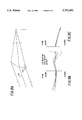
- FIGS. 1A and 1B are a front and a rear perspective view of a lenslet formed in accord with the teachings of the present invention
- FIG. 2 is a sectioned view taken along the section lines A--A of the lenslet of FIG. 1B;
- FIGS. 3A and 3B illustrates an aperture array positioned over a lenslet array with the spherical surface of each lenslet defined with topographical lines with the lenslets physical centers diverging with respect to photosensor centers in 3A and converging with respect to the photosensor centers in 3B;
- FIG. 4 illustrates, in a cross section view, an image sensor in accordance with the teachings of the present invention having an array of field stops and an array of aperture stops positioned in front of a lenslet array and photosensor array;
- FIG. 5 illustrates, in a cross section view, an image sensor in accordance with the teachings of the present invention having an array of field stops positioned in front of a lenslet array and photosensor array and an array of aperture stops positioned between the lenslet array and the photosensor array;
- FIGS. 6A, 6B, and 6C illustrate a cross section of, the portion of a lenslet associated with a 0 degree field angle, the associated tangential, and saggital ray aberration curves, respectively;
- FIGS. 7A, 7B, and 7C illustrate a cross section of, the portion of a lenslet associated with a 14 degree field angle, the associated tangential, and saggital ray aberration curves, respectively;
- FIGS. 8A, 8B, and 8C illustrate a cross section of, the portion of a lenslet associated with a 20 degree field angle, the associated tangential, and saggital ray aberration curves, respectively.
- the lenslet 10 is one element of a lenslet array that is formed with a number of lenslets.
- Each lenslet 10 is formed with a diffractive surface 18 formed on a refractive, spherical surface 20.
- Opposite the diffractive surface 18 is a second surface 22 that is an aspheric surface.
- the faceted surface of the diffractive surface 18 is seen more clearly in the cross-section of FIG. 2.
- the second surface is convex and transforms to a concave surface at the radius 12.
- the second surface 22 defines a polynomial asphere which exhibits an inflection at the radius 16. Both the first and the second surfaces are substantially perpendicular to the optical axis 24 of the lenslet 10.
- the lenslet 10 may be formed of optical glass such as BK7, quartz, injection molded plastic, or an epoxy replica.
- incident light rays 30 pass through an aperture stop array 40 and are focused onto a focal plane 50 by the lenslet 10.
- the diffractive/refractive surface comprised of 18 and 20 correct the chromatic aberrations and provide the majority of the focusing power while the aspheric surface 22 provides for correction of field dependent aberrations such as petzval curvature, astigmatism, and coma.
- the lens has an F# of 2.0 and a FL of 0.5 mm, but generally could be from 0.4 to 2.0 mm FL.
- the individual lenslets 10 of FIGS. 1 and 2 are segmented and formed into a lenslet array 60.
- the lenslet array 60 is formed with the lenslets 10 being associated with corresponding photosensor sites 72 (shown more clearly in FIG. 4).
- the mechanical center of the optical axis 24 of each lenslet 10 is displaced outward as a function of its radial distance from the optical axis of the central lenslet while in FIG. 3B, the optical axes are displaced inward.
- the lines 15 appearing around the optical axis 24 of each lenslet 10 are topographical lines generally indicating changes in height of the lenslet's surface.
- An array of aperture stops 26 fills the areas between the lenslets 10 to prevent light from reaching the sensor that will be discussed with respect to FIG. 4.
- the array depicted in FIGS. 3A and 3B represent only a small portion of an array that would be used in an actual camera. In an actual implementation approximately 260 ⁇ 214 to 1500 ⁇ 1000 lenslets are used to form the array 60. This invention does not form the lenslet array with the optical axis of each lenslet, and in turn the lenslet itself, aligned directly over a respective photosite in the CCD device.
- lenslets are displaced so as to form the image on a regularly spaced array of photosensors
- Other configurations of the lenslets may be used such as forming the outer periphery of each lenslet as a square, hexagon, or circle, without detracting from the invention.
- the reason that the invention uses only portions of the lenslets is that only a fraction of the lenslet is used for a particular angular field of view for an associated pixel of the group of three pixels for the color application.
- FIG. 4 is a cross-section taken along the section line 4--4 in FIGS. 3A and 3B, illustrating the lenslet array 60 positioned over an image photosensor array 70 that may be a CCD array having a number of photosensitive sites 72 corresponding in number to at least the number of lenslets forming the array 60. In a three color environment up to three photosensitive sites would be formed under each corresponding lenslet.
- the lenslet array 60 is maintained a distance apart from the surfaces of the photosensors by spacers 74 that may also serve the function of being baffles.
- the aperture stop array 40 in combination with the baffles 74 and the field stop array 42 limit the field of view of any particular photosensor so that it does not overlap the field of view of it neighbors by a large amount.
- the field stop array 42 is positioned approximately 0.5 mm to 2 mm from the surface of the lenslet array 60.
- the center of the apertures in the aperture stop array and field stop array, 40 and 42, respectively are aligned to the center of the field of view of a corresponding lenslet.
- the spacing of the centers increases as a function of each lenslet's field angle from the center of the array causing the aperture stop array to be slightly larger than the associated lenslet array.
- the combination of the aperture stop array 40 with the field stop array 42 and a given lenslet focal length determines the field of view for a photosensitive site 72.
- the lenslet array 60 can be formed of etched quartz, or an epoxy replica on a glass substrate.
- the lenslets 10, combined with the appropriate field and aperture stop form images of a small segment of the field of view on photosensitive site 72.
- the light incident on a lenslet 10 is concentrated onto the active pixel area.
- any camera system incorporating the present invention can be extremely compact and flat.
- the camera can work in black and white or in color if three pixels with color filters are formed on each pixel are used.
- An array of aspheric lenslets can be used to form images on the detector array.
- the aforementioned embodiment does not correct for the variation in focal length as a function of wavelength since the lens element is formed from a single refractive material therefore the spot size of the incident light varies as a function of color.
- An improved optical design including a diffractive/refractive hybrid lens is used to correct the chromatic aberration in a single material.
- n diff and element power distribution can be calculated.
- the negative n diff of the diffractive surface allows for achromatization of single element hybrid refractive/diffractive lenses utilizing a positive focal length diffractive and refractive component. It also decreases the focal length and F/# required of the doublet component lenses because a refractive doublet consists of a positive crown (low dispersion) lens with a shorter focal length and smaller F/# than is required for a single element lens and a negative flint element which increases the doublet focal length to the correct value and compensates for the dispersion of the positive lens. This effect also decreases the size and weight of the positive element of a hybrid refractive/diffractive element.
- substrates such as quartz, or optical glass such as BK7, or utilize epoxy replicas on glass substrates.
- diffractive/refractive hybrid achromatization enables the use of diffractive surfaces with longer focal lengths and higher F/#'s.
- the diffractive lenslets 10 are shown in FIGS. 6A, 7A, and 8A, for the on-axis, 16 degrees, and full field of view. To be noted in a comparison of these figs is that the mechanical optical axis 24 is moving radially outwards as a function of field angle while the local optical axis 25 is incident normal to the plane of the photodetector array.
- the opaque mask 16 acts as the aperture stop for the system as well as limiting the field of view of a given photosensor
- FIGS. 6B, 6C; 7B, 7C; and 8B, 8C represent the tangential and saggital ray aberration curves for their respective lenslets. It is noteworthy that the overall spot size, including chromatic aberration, is approximately 10 microns which is a typical photodetector size.
- the solid lines represent a wavelength of 546.1 nm, the dotted lines represent a wavelength of 656.1 nm, and the dotted and dashed lines represent a wavelength of 460.0 nm which represent light in the green, red, and blue, wavelengths.
- the following table lists the optical design parameters for three array elements at 0, 16, and 26 degrees.
- the array elements at the intermediate field angles can be interpolated from these values.
Landscapes
- Physics & Mathematics (AREA)
- General Physics & Mathematics (AREA)
- Optics & Photonics (AREA)
- Color Television Image Signal Generators (AREA)
- Lenses (AREA)
- Optical Filters (AREA)
- Solid State Image Pick-Up Elements (AREA)
- Transforming Light Signals Into Electric Signals (AREA)
- Diffracting Gratings Or Hologram Optical Elements (AREA)
Priority Applications (3)
| Application Number | Priority Date | Filing Date | Title |
|---|---|---|---|
| US08/663,887 US5751492A (en) | 1996-06-14 | 1996-06-14 | Diffractive/Refractive lenslet array incorporating a second aspheric surface |
| EP97108793A EP0813079A3 (en) | 1996-06-14 | 1997-06-02 | A diffractive/refractive lenslet array incorporating a second aspheric surface |
| JP15822397A JPH1084104A (ja) | 1996-06-14 | 1997-06-16 | イメージセンサ |
Applications Claiming Priority (1)
| Application Number | Priority Date | Filing Date | Title |
|---|---|---|---|
| US08/663,887 US5751492A (en) | 1996-06-14 | 1996-06-14 | Diffractive/Refractive lenslet array incorporating a second aspheric surface |
Publications (1)
| Publication Number | Publication Date |
|---|---|
| US5751492A true US5751492A (en) | 1998-05-12 |
Family
ID=24663642
Family Applications (1)
| Application Number | Title | Priority Date | Filing Date |
|---|---|---|---|
| US08/663,887 Expired - Lifetime US5751492A (en) | 1996-06-14 | 1996-06-14 | Diffractive/Refractive lenslet array incorporating a second aspheric surface |
Country Status (3)
| Country | Link |
|---|---|
| US (1) | US5751492A (ja) |
| EP (1) | EP0813079A3 (ja) |
| JP (1) | JPH1084104A (ja) |
Cited By (40)
| Publication number | Priority date | Publication date | Assignee | Title |
|---|---|---|---|---|
| US6069741A (en) * | 1997-03-31 | 2000-05-30 | Ricoh Company, Ltd. | Optical device having aperture arrays for shielding light |
| US20020075450A1 (en) * | 2000-11-30 | 2002-06-20 | Michiharu Aratani | Compound eye imaging system, imaging device, and electronic equipment |
| US20030038889A1 (en) * | 2001-08-23 | 2003-02-27 | Eastman Kodak Company | Method and apparatus for creating a preselected lenticular image |
| US6552809B1 (en) * | 2000-09-18 | 2003-04-22 | Institut National D'optique | Position encoding optical device and method |
| US20030086013A1 (en) * | 2001-11-02 | 2003-05-08 | Michiharu Aratani | Compound eye image-taking system and apparatus with the same |
| US6635941B2 (en) | 2001-03-21 | 2003-10-21 | Canon Kabushiki Kaisha | Structure of semiconductor device with improved reliability |
| US20040012698A1 (en) * | 2001-03-05 | 2004-01-22 | Yasuo Suda | Image pickup model and image pickup device |
| US20040119104A1 (en) * | 2002-12-20 | 2004-06-24 | Eastman Kodak Company | Imaging system having extended useful latitude |
| US6765617B1 (en) * | 1997-11-14 | 2004-07-20 | Tangen Reidar E | Optoelectronic camera and method for image formatting in the same |
| EP1447648A1 (en) * | 2003-02-12 | 2004-08-18 | Mitutoyo Corporation | Optical Encoder |
| US20040173737A1 (en) * | 2003-02-12 | 2004-09-09 | Mitutoyo Corporation | Optical configuration for imaging-type optical encoders |
| US20040179834A1 (en) * | 2003-03-14 | 2004-09-16 | Eastman Kodak Company | Camera using beam splitter with micro-lens image amplification |
| US20050046734A1 (en) * | 2003-08-26 | 2005-03-03 | Eastman Kodak Company | Photographic film cartridge or cassette systems with microlens |
| US20060163449A1 (en) * | 2005-01-26 | 2006-07-27 | Mark Butterworth | Planar fly's eye detector |
| US20090021837A1 (en) * | 2007-07-18 | 2009-01-22 | Funai Electric Co., Ltd. | Compound-Eye Imaging Device |
| US20090086301A1 (en) * | 2004-09-27 | 2009-04-02 | Idc, Llc | Display element having filter material diffused in a substrate of the display element |
| US20090236505A1 (en) * | 2005-09-19 | 2009-09-24 | Nereo Pallaro | Multifunctional optical sensor comprising a photodetectors matrix coupled to a microlenses matrix |
| US20100157406A1 (en) * | 2008-12-19 | 2010-06-24 | Qualcomm Mems Technologies, Inc. | System and method for matching light source emission to display element reflectivity |
| US20100245975A1 (en) * | 2004-09-27 | 2010-09-30 | Qualcomm Mems Technologies, Inc. | Display device having an array of spatial light modulators with integrated color filters |
| US20100259728A1 (en) * | 2009-04-10 | 2010-10-14 | Sumitomo Electric Industries, Ltd. | Optical combiner and image projector using the optical combiner |
| US20100259729A1 (en) * | 2009-04-10 | 2010-10-14 | Sumitomo Electric Industries, Ltd. | Optical combiner and image projector using the optical combiner |
| US20110090136A1 (en) * | 2004-03-06 | 2011-04-21 | Qualcomm Mems Technologies, Inc. | Method and system for color optimization in a display |
| US20110115916A1 (en) * | 2009-11-16 | 2011-05-19 | Eiji Yafuso | System for mosaic image acquisition |
| US8061882B2 (en) | 2006-10-06 | 2011-11-22 | Qualcomm Mems Technologies, Inc. | Illumination device with built-in light coupler |
| US20120188391A1 (en) * | 2011-01-25 | 2012-07-26 | Scott Smith | Array camera having lenses with independent fields of view |
| US8362987B2 (en) | 2004-09-27 | 2013-01-29 | Qualcomm Mems Technologies, Inc. | Method and device for manipulating color in a display |
| US8670171B2 (en) | 2010-10-18 | 2014-03-11 | Qualcomm Mems Technologies, Inc. | Display having an embedded microlens array |
| US8798425B2 (en) | 2007-12-07 | 2014-08-05 | Qualcomm Mems Technologies, Inc. | Decoupled holographic film and diffuser |
| US20140267764A1 (en) * | 2013-03-14 | 2014-09-18 | Drs Rsta, Inc. | Single element radiometric lens |
| US8848294B2 (en) | 2010-05-20 | 2014-09-30 | Qualcomm Mems Technologies, Inc. | Method and structure capable of changing color saturation |
| US8872085B2 (en) | 2006-10-06 | 2014-10-28 | Qualcomm Mems Technologies, Inc. | Display device having front illuminator with turning features |
| US8979349B2 (en) | 2009-05-29 | 2015-03-17 | Qualcomm Mems Technologies, Inc. | Illumination devices and methods of fabrication thereof |
| US9019590B2 (en) | 2004-02-03 | 2015-04-28 | Qualcomm Mems Technologies, Inc. | Spatial light modulator with integrated optical compensation structure |
| US9019183B2 (en) | 2006-10-06 | 2015-04-28 | Qualcomm Mems Technologies, Inc. | Optical loss structure integrated in an illumination apparatus |
| US9025235B2 (en) | 2002-12-25 | 2015-05-05 | Qualcomm Mems Technologies, Inc. | Optical interference type of color display having optical diffusion layer between substrate and electrode |
| US9391105B2 (en) | 2011-07-08 | 2016-07-12 | Panasonic Intellectual Property Management Co., Ltd. | Solid-state imaging device and imaging apparatus |
| US10215362B2 (en) | 2014-12-25 | 2019-02-26 | Nichia Corporation | Light source apparatus with lens array |
| US11333748B2 (en) | 2018-09-17 | 2022-05-17 | Waymo Llc | Array of light detectors with corresponding array of optical elements |
| US12038310B2 (en) | 2019-11-15 | 2024-07-16 | Renishaw Plc | Encoder apparatus with readhead having circuit board and a folded sheet-metal structure to support a light emitting element |
| US12072216B2 (en) | 2019-11-15 | 2024-08-27 | Renishaw Plc | Encoder apparatus and readhead |
Families Citing this family (9)
| Publication number | Priority date | Publication date | Assignee | Title |
|---|---|---|---|---|
| FI114520B (fi) * | 2002-12-20 | 2004-10-29 | Nokia Corp | Värikuvantamisjärjestelmä ja menetelmä värikuvantamisjärjestelmässä |
| US7511749B2 (en) * | 2003-12-18 | 2009-03-31 | Aptina Imaging Corporation | Color image sensor having imaging element array forming images on respective regions of sensor elements |
| DE102004003013B3 (de) * | 2004-01-20 | 2005-06-02 | Fraunhofer-Gesellschaft zur Förderung der angewandten Forschung e.V. | Bilderfassungssystem und dessen Verwendung |
| EP1712087B1 (en) * | 2004-01-26 | 2021-03-10 | DigitalOptics Corporation | Thin camera having sub-pixel resolution |
| US7271963B2 (en) * | 2005-03-07 | 2007-09-18 | Avago Technologies Ecbu Ip (Singapore) Pte. Ltd. | Bi-curvature lens for light emitting diodes and photo detectors |
| JP2007329714A (ja) | 2006-06-08 | 2007-12-20 | Funai Electric Co Ltd | 複眼撮像装置 |
| DE102013226196A1 (de) * | 2013-12-17 | 2015-06-18 | Volkswagen Aktiengesellschaft | Optisches Sensorsystem |
| CA3225168A1 (en) | 2014-05-28 | 2015-12-03 | Inoptec Limited Zweigniederlassung Deutschland | Electronic spectacles |
| IL284740B2 (en) * | 2021-07-08 | 2023-05-01 | Elbit Systems Electro Optics Elop Ltd | Optical correction component for coherent beam combining systems and coherent beam combining methods and systems using an optical correction component |
Citations (38)
| Publication number | Priority date | Publication date | Assignee | Title |
|---|---|---|---|---|
| US3765741A (en) * | 1970-12-26 | 1973-10-16 | Konishiroku Photo Ind | Method of forming three-dimensional images using multi-image hologram |
| US3910683A (en) * | 1970-07-28 | 1975-10-07 | Minolta Camera Kk | Optical low-pass filter |
| US4009939A (en) * | 1974-06-05 | 1977-03-01 | Minolta Camera Kabushiki Kaisha | Double layered optical low pass filter permitting improved image resolution |
| US4083627A (en) * | 1975-01-20 | 1978-04-11 | Minolta Camera Kabushiki Kaisha | Two dimensional optical phase grating filter |
| US4093346A (en) * | 1973-07-13 | 1978-06-06 | Minolta Camera Kabushiki Kaisha | Optical low pass filter |
| US4318123A (en) * | 1980-06-05 | 1982-03-02 | Rca Corporation | Solid-state, color-encoding television camera |
| US4323925A (en) * | 1980-07-07 | 1982-04-06 | Avco Everett Research Laboratory, Inc. | Method and apparatus for arraying image sensor modules |
| US4377753A (en) * | 1981-06-01 | 1983-03-22 | Eastman Kodak Company | High resolution optical-addressing device and electronic scanner and/or printer apparatus employing such device |
| US4689291A (en) * | 1985-08-30 | 1987-08-25 | Xerox Corporation | Pedestal-type microlens fabrication process |
| US4708436A (en) * | 1985-07-12 | 1987-11-24 | Rca Corporation | Optical imager with diffractive lenticular array |
| US4733096A (en) * | 1985-12-19 | 1988-03-22 | Ricoh Company, Ltd. | Directly detectable image sensor employing a lens array and method of producing the same |
| US4795236A (en) * | 1984-12-25 | 1989-01-03 | Sony Corporation | Optical low pass filter utilizing a phase grating |
| US4878737A (en) * | 1986-12-24 | 1989-11-07 | Sony Corp. | Optical low-pass filter |
| US4905037A (en) * | 1986-03-13 | 1990-02-27 | Brother Kogyo Kabushiki Kaisha | Image transfer system |
| US4989985A (en) * | 1988-09-19 | 1991-02-05 | Xerox Corporation | Densitometer for measuring specular reflectivity |
| US4989959A (en) * | 1989-06-12 | 1991-02-05 | Polaroid Corporation | Anti-aliasing optical system with pyramidal transparent structure |
| US4994664A (en) * | 1989-03-27 | 1991-02-19 | Massachusetts Institute Of Technology | Optically coupled focal plane arrays using lenslets and multiplexers |
| US4998800A (en) * | 1988-04-04 | 1991-03-12 | Nippon Hoso Kyokai | Optical low pass filter |
| US5004901A (en) * | 1987-06-04 | 1991-04-02 | Mitsubishi Denki Kabushiki Kaisha | Current mirror amplifier for use in an optical data medium driving apparatus and servo-circuit |
| US5029010A (en) * | 1988-11-28 | 1991-07-02 | Canon Kabushiki Kaisha | Imaging system with optical low-pass filter |
| US5046827A (en) * | 1989-07-20 | 1991-09-10 | Honeywell Inc. | Optical reconstruction filter for color mosaic displays |
| US5076687A (en) * | 1990-08-28 | 1991-12-31 | Massachusetts Institute Of Technology | Optical ranging apparatus |
| US5121213A (en) * | 1987-02-25 | 1992-06-09 | Olympus Optical Co., Ltd. | Imaging system having a blurring optical element for minimizing moire phenomenon |
| US5151790A (en) * | 1990-07-23 | 1992-09-29 | Fuji Photo Film Co., Ltd. | Image pickup device for stabilizing optical aberrations |
| US5187358A (en) * | 1989-02-15 | 1993-02-16 | Canon Kabushiki Kaisha | Image reading device having a telecentric optical system and a blazed diffraction grating |
| US5233174A (en) * | 1992-03-11 | 1993-08-03 | Hughes Danbury Optical Systems, Inc. | Wavefront sensor having a lenslet array as a null corrector |
| US5233431A (en) * | 1990-10-26 | 1993-08-03 | Fuji Photo Film Co., Ltd. | Image pickup device |
| US5280388A (en) * | 1990-04-27 | 1994-01-18 | Matsushita Electric Industrial Co., Ltd. | Wavelength selective phase grating optical low-pass filter |
| US5294993A (en) * | 1992-04-10 | 1994-03-15 | Opton Corporation | Method and apparatus for using monochrome images to form a color image |
| US5309239A (en) * | 1991-07-11 | 1994-05-03 | U.S. Philips Corporation | Image pick-up device |
| US5322998A (en) * | 1993-03-31 | 1994-06-21 | Eastman Kodak Company | Conical blur filter for reducing artifacts in imaging apparatus |
| US5340978A (en) * | 1992-09-30 | 1994-08-23 | Lsi Logic Corporation | Image-sensing display panels with LCD display panel and photosensitive element array |
| US5349471A (en) * | 1993-02-16 | 1994-09-20 | The University Of Rochester | Hybrid refractive/diffractive achromatic lens for optical data storage systems |
| US5471515A (en) * | 1994-01-28 | 1995-11-28 | California Institute Of Technology | Active pixel sensor with intra-pixel charge transfer |
| US5497269A (en) * | 1992-06-25 | 1996-03-05 | Lockheed Missiles And Space Company, Inc. | Dispersive microlens |
| US5504621A (en) * | 1992-08-28 | 1996-04-02 | Matsushita Electric Industrial Co., Ltd. | Two-dimensional optical low-pass filter |
| JPH08107194A (ja) * | 1994-10-03 | 1996-04-23 | Fuji Photo Optical Co Ltd | 固体撮像装置 |
| US5529936A (en) * | 1992-09-30 | 1996-06-25 | Lsi Logic Corporation | Method of etching a lens for a semiconductor solid state image sensor |
Family Cites Families (3)
| Publication number | Priority date | Publication date | Assignee | Title |
|---|---|---|---|---|
| JPS5788113U (ja) * | 1980-11-20 | 1982-05-31 | ||
| US5412506A (en) * | 1992-03-09 | 1995-05-02 | At&T Corp. | Free-space optical interconnection arrangement |
| GB9301405D0 (en) * | 1993-01-25 | 1993-03-17 | Philips Electronics Uk Ltd | An image sensor |
-
1996
- 1996-06-14 US US08/663,887 patent/US5751492A/en not_active Expired - Lifetime
-
1997
- 1997-06-02 EP EP97108793A patent/EP0813079A3/en not_active Withdrawn
- 1997-06-16 JP JP15822397A patent/JPH1084104A/ja active Pending
Patent Citations (39)
| Publication number | Priority date | Publication date | Assignee | Title |
|---|---|---|---|---|
| US3910683A (en) * | 1970-07-28 | 1975-10-07 | Minolta Camera Kk | Optical low-pass filter |
| US3765741A (en) * | 1970-12-26 | 1973-10-16 | Konishiroku Photo Ind | Method of forming three-dimensional images using multi-image hologram |
| US4093346A (en) * | 1973-07-13 | 1978-06-06 | Minolta Camera Kabushiki Kaisha | Optical low pass filter |
| US4009939A (en) * | 1974-06-05 | 1977-03-01 | Minolta Camera Kabushiki Kaisha | Double layered optical low pass filter permitting improved image resolution |
| US4083627A (en) * | 1975-01-20 | 1978-04-11 | Minolta Camera Kabushiki Kaisha | Two dimensional optical phase grating filter |
| US4318123A (en) * | 1980-06-05 | 1982-03-02 | Rca Corporation | Solid-state, color-encoding television camera |
| US4323925A (en) * | 1980-07-07 | 1982-04-06 | Avco Everett Research Laboratory, Inc. | Method and apparatus for arraying image sensor modules |
| US4377753A (en) * | 1981-06-01 | 1983-03-22 | Eastman Kodak Company | High resolution optical-addressing device and electronic scanner and/or printer apparatus employing such device |
| US4795236A (en) * | 1984-12-25 | 1989-01-03 | Sony Corporation | Optical low pass filter utilizing a phase grating |
| US4708436A (en) * | 1985-07-12 | 1987-11-24 | Rca Corporation | Optical imager with diffractive lenticular array |
| US4689291A (en) * | 1985-08-30 | 1987-08-25 | Xerox Corporation | Pedestal-type microlens fabrication process |
| US4733096A (en) * | 1985-12-19 | 1988-03-22 | Ricoh Company, Ltd. | Directly detectable image sensor employing a lens array and method of producing the same |
| US4905037A (en) * | 1986-03-13 | 1990-02-27 | Brother Kogyo Kabushiki Kaisha | Image transfer system |
| US4878737A (en) * | 1986-12-24 | 1989-11-07 | Sony Corp. | Optical low-pass filter |
| US5121213A (en) * | 1987-02-25 | 1992-06-09 | Olympus Optical Co., Ltd. | Imaging system having a blurring optical element for minimizing moire phenomenon |
| US5004901A (en) * | 1987-06-04 | 1991-04-02 | Mitsubishi Denki Kabushiki Kaisha | Current mirror amplifier for use in an optical data medium driving apparatus and servo-circuit |
| US4998800A (en) * | 1988-04-04 | 1991-03-12 | Nippon Hoso Kyokai | Optical low pass filter |
| US4989985A (en) * | 1988-09-19 | 1991-02-05 | Xerox Corporation | Densitometer for measuring specular reflectivity |
| US5029010A (en) * | 1988-11-28 | 1991-07-02 | Canon Kabushiki Kaisha | Imaging system with optical low-pass filter |
| US5187358A (en) * | 1989-02-15 | 1993-02-16 | Canon Kabushiki Kaisha | Image reading device having a telecentric optical system and a blazed diffraction grating |
| US4994664A (en) * | 1989-03-27 | 1991-02-19 | Massachusetts Institute Of Technology | Optically coupled focal plane arrays using lenslets and multiplexers |
| US4989959A (en) * | 1989-06-12 | 1991-02-05 | Polaroid Corporation | Anti-aliasing optical system with pyramidal transparent structure |
| US5046827A (en) * | 1989-07-20 | 1991-09-10 | Honeywell Inc. | Optical reconstruction filter for color mosaic displays |
| US5046827C1 (en) * | 1989-07-20 | 2001-08-07 | Honeywell Inc | Optical reconstruction filter for color mosaic displays |
| US5280388A (en) * | 1990-04-27 | 1994-01-18 | Matsushita Electric Industrial Co., Ltd. | Wavelength selective phase grating optical low-pass filter |
| US5151790A (en) * | 1990-07-23 | 1992-09-29 | Fuji Photo Film Co., Ltd. | Image pickup device for stabilizing optical aberrations |
| US5076687A (en) * | 1990-08-28 | 1991-12-31 | Massachusetts Institute Of Technology | Optical ranging apparatus |
| US5233431A (en) * | 1990-10-26 | 1993-08-03 | Fuji Photo Film Co., Ltd. | Image pickup device |
| US5309239A (en) * | 1991-07-11 | 1994-05-03 | U.S. Philips Corporation | Image pick-up device |
| US5233174A (en) * | 1992-03-11 | 1993-08-03 | Hughes Danbury Optical Systems, Inc. | Wavefront sensor having a lenslet array as a null corrector |
| US5294993A (en) * | 1992-04-10 | 1994-03-15 | Opton Corporation | Method and apparatus for using monochrome images to form a color image |
| US5497269A (en) * | 1992-06-25 | 1996-03-05 | Lockheed Missiles And Space Company, Inc. | Dispersive microlens |
| US5504621A (en) * | 1992-08-28 | 1996-04-02 | Matsushita Electric Industrial Co., Ltd. | Two-dimensional optical low-pass filter |
| US5340978A (en) * | 1992-09-30 | 1994-08-23 | Lsi Logic Corporation | Image-sensing display panels with LCD display panel and photosensitive element array |
| US5529936A (en) * | 1992-09-30 | 1996-06-25 | Lsi Logic Corporation | Method of etching a lens for a semiconductor solid state image sensor |
| US5349471A (en) * | 1993-02-16 | 1994-09-20 | The University Of Rochester | Hybrid refractive/diffractive achromatic lens for optical data storage systems |
| US5322998A (en) * | 1993-03-31 | 1994-06-21 | Eastman Kodak Company | Conical blur filter for reducing artifacts in imaging apparatus |
| US5471515A (en) * | 1994-01-28 | 1995-11-28 | California Institute Of Technology | Active pixel sensor with intra-pixel charge transfer |
| JPH08107194A (ja) * | 1994-10-03 | 1996-04-23 | Fuji Photo Optical Co Ltd | 固体撮像装置 |
Non-Patent Citations (4)
| Title |
|---|
| "Visible Array Detectors" by Timothy J. Tredwell, from Handbook of Optics, vol. 1, Fundamentals, Techniques, & Design, Second Edition, Chapter 22, pp. 32-34. |
| Toshio Honda, International Conference on Applications of Optical Holography, SPIE The International Society for Optical Engineering, vol. 2577, Jun. 5, 1995. * |
| Toshio Honda, International Conference on Applications of Optical Holography, SPIE--The International Society for Optical Engineering, vol. 2577, Jun. 5, 1995. |
| Visible Array Detectors by Timothy J. Tredwell, from Handbook of Optics, vol. 1, Fundamentals, Techniques, & Design, Second Edition, Chapter 22, pp. 32 34. * |
Cited By (60)
| Publication number | Priority date | Publication date | Assignee | Title |
|---|---|---|---|---|
| US6069741A (en) * | 1997-03-31 | 2000-05-30 | Ricoh Company, Ltd. | Optical device having aperture arrays for shielding light |
| US6765617B1 (en) * | 1997-11-14 | 2004-07-20 | Tangen Reidar E | Optoelectronic camera and method for image formatting in the same |
| US6552809B1 (en) * | 2000-09-18 | 2003-04-22 | Institut National D'optique | Position encoding optical device and method |
| US20020075450A1 (en) * | 2000-11-30 | 2002-06-20 | Michiharu Aratani | Compound eye imaging system, imaging device, and electronic equipment |
| US20040012698A1 (en) * | 2001-03-05 | 2004-01-22 | Yasuo Suda | Image pickup model and image pickup device |
| US6893941B2 (en) | 2001-03-21 | 2005-05-17 | Canon Kabushiki Kaisha | Semiconductor device and its manufacture method |
| US6635941B2 (en) | 2001-03-21 | 2003-10-21 | Canon Kabushiki Kaisha | Structure of semiconductor device with improved reliability |
| US20030038889A1 (en) * | 2001-08-23 | 2003-02-27 | Eastman Kodak Company | Method and apparatus for creating a preselected lenticular image |
| US6894719B2 (en) | 2001-08-23 | 2005-05-17 | Eastman Kodak Company | Method and apparatus for creating a preselected lenticular image |
| US20030086013A1 (en) * | 2001-11-02 | 2003-05-08 | Michiharu Aratani | Compound eye image-taking system and apparatus with the same |
| US20040119104A1 (en) * | 2002-12-20 | 2004-06-24 | Eastman Kodak Company | Imaging system having extended useful latitude |
| US7423679B2 (en) | 2002-12-20 | 2008-09-09 | Eastman Kodak Company | Imaging system having extended useful latitude |
| US9025235B2 (en) | 2002-12-25 | 2015-05-05 | Qualcomm Mems Technologies, Inc. | Optical interference type of color display having optical diffusion layer between substrate and electrode |
| EP1447648A1 (en) * | 2003-02-12 | 2004-08-18 | Mitutoyo Corporation | Optical Encoder |
| US20040173737A1 (en) * | 2003-02-12 | 2004-09-09 | Mitutoyo Corporation | Optical configuration for imaging-type optical encoders |
| US20070018084A1 (en) * | 2003-02-12 | 2007-01-25 | Mitutoyo Corporation | Optical configuration for imaging-type optical encoders |
| US7186969B2 (en) | 2003-02-12 | 2007-03-06 | Mitutoyo Corporation | Optical configuration for imaging-type optical encoders |
| US7435945B2 (en) | 2003-02-12 | 2008-10-14 | Mitutoyo Corporation | Optical configuration for imaging-type optical encoders |
| US6801719B1 (en) | 2003-03-14 | 2004-10-05 | Eastman Kodak Company | Camera using beam splitter with micro-lens image amplification |
| US20040179834A1 (en) * | 2003-03-14 | 2004-09-16 | Eastman Kodak Company | Camera using beam splitter with micro-lens image amplification |
| US7310477B2 (en) | 2003-08-26 | 2007-12-18 | Eastman Kodak Company | Photographic film cartridge or cassette systems with microlens |
| US20050046734A1 (en) * | 2003-08-26 | 2005-03-03 | Eastman Kodak Company | Photographic film cartridge or cassette systems with microlens |
| US9019590B2 (en) | 2004-02-03 | 2015-04-28 | Qualcomm Mems Technologies, Inc. | Spatial light modulator with integrated optical compensation structure |
| US20070215797A1 (en) * | 2004-02-11 | 2007-09-20 | Mitutoyo Corporation | Photoelectric Encoder |
| US7570433B2 (en) | 2004-02-11 | 2009-08-04 | Mitutoyo Corporation | Photoelectric encoder |
| US8094362B2 (en) | 2004-03-06 | 2012-01-10 | Qualcomm Mems Technologies, Inc. | Method and system for color optimization in a display |
| US20110090136A1 (en) * | 2004-03-06 | 2011-04-21 | Qualcomm Mems Technologies, Inc. | Method and system for color optimization in a display |
| US20090086301A1 (en) * | 2004-09-27 | 2009-04-02 | Idc, Llc | Display element having filter material diffused in a substrate of the display element |
| US20100245975A1 (en) * | 2004-09-27 | 2010-09-30 | Qualcomm Mems Technologies, Inc. | Display device having an array of spatial light modulators with integrated color filters |
| US8362987B2 (en) | 2004-09-27 | 2013-01-29 | Qualcomm Mems Technologies, Inc. | Method and device for manipulating color in a display |
| US8344377B2 (en) * | 2004-09-27 | 2013-01-01 | Qualcomm Mems Technologies, Inc. | Display element having filter material diffused in a substrate of the display element |
| US20060163449A1 (en) * | 2005-01-26 | 2006-07-27 | Mark Butterworth | Planar fly's eye detector |
| US7375312B2 (en) * | 2005-01-26 | 2008-05-20 | Avago Technologies Ecbu Ip Pte Ltd | Planar fly's eye detector |
| US20090236505A1 (en) * | 2005-09-19 | 2009-09-24 | Nereo Pallaro | Multifunctional optical sensor comprising a photodetectors matrix coupled to a microlenses matrix |
| US9019183B2 (en) | 2006-10-06 | 2015-04-28 | Qualcomm Mems Technologies, Inc. | Optical loss structure integrated in an illumination apparatus |
| US8061882B2 (en) | 2006-10-06 | 2011-11-22 | Qualcomm Mems Technologies, Inc. | Illumination device with built-in light coupler |
| US8872085B2 (en) | 2006-10-06 | 2014-10-28 | Qualcomm Mems Technologies, Inc. | Display device having front illuminator with turning features |
| US7700904B2 (en) | 2007-07-18 | 2010-04-20 | Funai Electric Co., Ltd. | Compound-eye imaging device |
| US20090021837A1 (en) * | 2007-07-18 | 2009-01-22 | Funai Electric Co., Ltd. | Compound-Eye Imaging Device |
| US8798425B2 (en) | 2007-12-07 | 2014-08-05 | Qualcomm Mems Technologies, Inc. | Decoupled holographic film and diffuser |
| US20100157406A1 (en) * | 2008-12-19 | 2010-06-24 | Qualcomm Mems Technologies, Inc. | System and method for matching light source emission to display element reflectivity |
| US20100259728A1 (en) * | 2009-04-10 | 2010-10-14 | Sumitomo Electric Industries, Ltd. | Optical combiner and image projector using the optical combiner |
| US20100259729A1 (en) * | 2009-04-10 | 2010-10-14 | Sumitomo Electric Industries, Ltd. | Optical combiner and image projector using the optical combiner |
| US8403491B2 (en) | 2009-04-10 | 2013-03-26 | Sumitomo Electric Industries, Ltd. | Optical combiner and image projector using the optical combiner |
| US8098435B2 (en) * | 2009-04-10 | 2012-01-17 | Sumitomo Electric Industries, Ltd. | Optical combiner and image projector using the optical combiner |
| US9121979B2 (en) | 2009-05-29 | 2015-09-01 | Qualcomm Mems Technologies, Inc. | Illumination devices and methods of fabrication thereof |
| US8979349B2 (en) | 2009-05-29 | 2015-03-17 | Qualcomm Mems Technologies, Inc. | Illumination devices and methods of fabrication thereof |
| US20110115916A1 (en) * | 2009-11-16 | 2011-05-19 | Eiji Yafuso | System for mosaic image acquisition |
| US8848294B2 (en) | 2010-05-20 | 2014-09-30 | Qualcomm Mems Technologies, Inc. | Method and structure capable of changing color saturation |
| US8670171B2 (en) | 2010-10-18 | 2014-03-11 | Qualcomm Mems Technologies, Inc. | Display having an embedded microlens array |
| US20120188391A1 (en) * | 2011-01-25 | 2012-07-26 | Scott Smith | Array camera having lenses with independent fields of view |
| US9391105B2 (en) | 2011-07-08 | 2016-07-12 | Panasonic Intellectual Property Management Co., Ltd. | Solid-state imaging device and imaging apparatus |
| US20140267764A1 (en) * | 2013-03-14 | 2014-09-18 | Drs Rsta, Inc. | Single element radiometric lens |
| US9615036B2 (en) * | 2013-03-14 | 2017-04-04 | Drs Network & Imaging Systems, Llc | Single element radiometric lens |
| US20170160524A1 (en) * | 2013-03-14 | 2017-06-08 | Drs Network & Imaging Systems, Llc | Single element radiometric lens |
| US9869848B2 (en) * | 2013-03-14 | 2018-01-16 | Drs Network & Imaging Systems, Llc | Single element radiometric lens |
| US10215362B2 (en) | 2014-12-25 | 2019-02-26 | Nichia Corporation | Light source apparatus with lens array |
| US11333748B2 (en) | 2018-09-17 | 2022-05-17 | Waymo Llc | Array of light detectors with corresponding array of optical elements |
| US12038310B2 (en) | 2019-11-15 | 2024-07-16 | Renishaw Plc | Encoder apparatus with readhead having circuit board and a folded sheet-metal structure to support a light emitting element |
| US12072216B2 (en) | 2019-11-15 | 2024-08-27 | Renishaw Plc | Encoder apparatus and readhead |
Also Published As
| Publication number | Publication date |
|---|---|
| JPH1084104A (ja) | 1998-03-31 |
| EP0813079A2 (en) | 1997-12-17 |
| EP0813079A3 (en) | 1998-01-14 |
Similar Documents
| Publication | Publication Date | Title |
|---|---|---|
| US5751492A (en) | Diffractive/Refractive lenslet array incorporating a second aspheric surface | |
| US5696371A (en) | Diffractive/refractive lenslet array | |
| US5731899A (en) | Lenslet array system incorporating an integral field lens/reimager lenslet array | |
| US5822125A (en) | Lenslet array system | |
| EP0532267B1 (en) | Re-imaging optical system employing refractive and diffractive optical elements | |
| WO2021021671A1 (en) | Aperture-metasurface and hybrid refractive-metasurface imaging systems | |
| US5880879A (en) | Objective lens system utilizing diffractive optical element | |
| US8576489B2 (en) | Multihybrid artificial compound eye with varied ommatidia | |
| CN118295106A (zh) | 光学成像镜头 | |
| US20020118457A1 (en) | Wavefront coded imaging systems | |
| WO1998044374A1 (en) | Refractive/diffractive infrared imager and optics | |
| US5812322A (en) | Lenslet array system incorporating a field lenslet array | |
| US8736985B2 (en) | Photographic lens optical system | |
| KR20200026694A (ko) | 광각 이미징 렌즈 | |
| US6147815A (en) | Imaging optical system | |
| US5680252A (en) | Miniature hybrid optical imaging lens | |
| US11221468B2 (en) | Optical imaging module having a hyper-hemispherical field and controlled distortion and compatible with an outside environment | |
| JP3724520B2 (ja) | 赤外用光学系 | |
| US8432620B2 (en) | Photographic lens optical system | |
| JP7225047B2 (ja) | 撮像レンズおよび撮像装置 | |
| JP3467018B2 (ja) | 光学系及び光学機器 | |
| JPH10505432A (ja) | 高速光学システム | |
| US6563654B2 (en) | External pupil lens system | |
| SU1714562A1 (ru) | Инфракрасный объектив | |
| JPH10115776A (ja) | 撮像レンズ |
Legal Events
| Date | Code | Title | Description |
|---|---|---|---|
| AS | Assignment |
Owner name: EASTMAN KODAK COMPANY, NEW YORK Free format text: ASSIGNMENT OF ASSIGNORS INTEREST;ASSIGNOR:MEYERS, MARK M.;REEL/FRAME:008051/0906 Effective date: 19960613 |
|
| FEPP | Fee payment procedure |
Free format text: PAYOR NUMBER ASSIGNED (ORIGINAL EVENT CODE: ASPN); ENTITY STATUS OF PATENT OWNER: LARGE ENTITY |
|
| STCF | Information on status: patent grant |
Free format text: PATENTED CASE |
|
| FPAY | Fee payment |
Year of fee payment: 4 |
|
| FPAY | Fee payment |
Year of fee payment: 8 |
|
| FPAY | Fee payment |
Year of fee payment: 12 |
|
| AS | Assignment |
Owner name: CITICORP NORTH AMERICA, INC., AS AGENT, NEW YORK Free format text: SECURITY INTEREST;ASSIGNORS:EASTMAN KODAK COMPANY;PAKON, INC.;REEL/FRAME:028201/0420 Effective date: 20120215 |
|
| FEPP | Fee payment procedure |
Free format text: PAYER NUMBER DE-ASSIGNED (ORIGINAL EVENT CODE: RMPN); ENTITY STATUS OF PATENT OWNER: LARGE ENTITY Free format text: PAYOR NUMBER ASSIGNED (ORIGINAL EVENT CODE: ASPN); ENTITY STATUS OF PATENT OWNER: LARGE ENTITY |
|
| AS | Assignment |
Owner name: KODAK PHILIPPINES, LTD., NEW YORK Free format text: PATENT RELEASE;ASSIGNORS:CITICORP NORTH AMERICA, INC.;WILMINGTON TRUST, NATIONAL ASSOCIATION;REEL/FRAME:029913/0001 Effective date: 20130201 Owner name: EASTMAN KODAK INTERNATIONAL CAPITAL COMPANY, INC., NEW YORK Free format text: PATENT RELEASE;ASSIGNORS:CITICORP NORTH AMERICA, INC.;WILMINGTON TRUST, NATIONAL ASSOCIATION;REEL/FRAME:029913/0001 Effective date: 20130201 Owner name: QUALEX INC., NORTH CAROLINA Free format text: PATENT RELEASE;ASSIGNORS:CITICORP NORTH AMERICA, INC.;WILMINGTON TRUST, NATIONAL ASSOCIATION;REEL/FRAME:029913/0001 Effective date: 20130201 Owner name: KODAK AMERICAS, LTD., NEW YORK Free format text: PATENT RELEASE;ASSIGNORS:CITICORP NORTH AMERICA, INC.;WILMINGTON TRUST, NATIONAL ASSOCIATION;REEL/FRAME:029913/0001 Effective date: 20130201 Owner name: FAR EAST DEVELOPMENT LTD., NEW YORK Free format text: PATENT RELEASE;ASSIGNORS:CITICORP NORTH AMERICA, INC.;WILMINGTON TRUST, NATIONAL ASSOCIATION;REEL/FRAME:029913/0001 Effective date: 20130201 Owner name: PAKON, INC., INDIANA Free format text: PATENT RELEASE;ASSIGNORS:CITICORP NORTH AMERICA, INC.;WILMINGTON TRUST, NATIONAL ASSOCIATION;REEL/FRAME:029913/0001 Effective date: 20130201 Owner name: KODAK IMAGING NETWORK, INC., CALIFORNIA Free format text: PATENT RELEASE;ASSIGNORS:CITICORP NORTH AMERICA, INC.;WILMINGTON TRUST, NATIONAL ASSOCIATION;REEL/FRAME:029913/0001 Effective date: 20130201 Owner name: LASER-PACIFIC MEDIA CORPORATION, NEW YORK Free format text: PATENT RELEASE;ASSIGNORS:CITICORP NORTH AMERICA, INC.;WILMINGTON TRUST, NATIONAL ASSOCIATION;REEL/FRAME:029913/0001 Effective date: 20130201 Owner name: EASTMAN KODAK INTERNATIONAL CAPITAL COMPANY, INC., Free format text: PATENT RELEASE;ASSIGNORS:CITICORP NORTH AMERICA, INC.;WILMINGTON TRUST, NATIONAL ASSOCIATION;REEL/FRAME:029913/0001 Effective date: 20130201 Owner name: CREO MANUFACTURING AMERICA LLC, WYOMING Free format text: PATENT RELEASE;ASSIGNORS:CITICORP NORTH AMERICA, INC.;WILMINGTON TRUST, NATIONAL ASSOCIATION;REEL/FRAME:029913/0001 Effective date: 20130201 Owner name: KODAK PORTUGUESA LIMITED, NEW YORK Free format text: PATENT RELEASE;ASSIGNORS:CITICORP NORTH AMERICA, INC.;WILMINGTON TRUST, NATIONAL ASSOCIATION;REEL/FRAME:029913/0001 Effective date: 20130201 Owner name: KODAK AVIATION LEASING LLC, NEW YORK Free format text: PATENT RELEASE;ASSIGNORS:CITICORP NORTH AMERICA, INC.;WILMINGTON TRUST, NATIONAL ASSOCIATION;REEL/FRAME:029913/0001 Effective date: 20130201 Owner name: EASTMAN KODAK COMPANY, NEW YORK Free format text: PATENT RELEASE;ASSIGNORS:CITICORP NORTH AMERICA, INC.;WILMINGTON TRUST, NATIONAL ASSOCIATION;REEL/FRAME:029913/0001 Effective date: 20130201 Owner name: KODAK REALTY, INC., NEW YORK Free format text: PATENT RELEASE;ASSIGNORS:CITICORP NORTH AMERICA, INC.;WILMINGTON TRUST, NATIONAL ASSOCIATION;REEL/FRAME:029913/0001 Effective date: 20130201 Owner name: NPEC INC., NEW YORK Free format text: PATENT RELEASE;ASSIGNORS:CITICORP NORTH AMERICA, INC.;WILMINGTON TRUST, NATIONAL ASSOCIATION;REEL/FRAME:029913/0001 Effective date: 20130201 Owner name: FPC INC., CALIFORNIA Free format text: PATENT RELEASE;ASSIGNORS:CITICORP NORTH AMERICA, INC.;WILMINGTON TRUST, NATIONAL ASSOCIATION;REEL/FRAME:029913/0001 Effective date: 20130201 Owner name: KODAK (NEAR EAST), INC., NEW YORK Free format text: PATENT RELEASE;ASSIGNORS:CITICORP NORTH AMERICA, INC.;WILMINGTON TRUST, NATIONAL ASSOCIATION;REEL/FRAME:029913/0001 Effective date: 20130201 |
|
| AS | Assignment |
Owner name: INTELLECTUAL VENTURES FUND 83 LLC, NEVADA Free format text: ASSIGNMENT OF ASSIGNORS INTEREST;ASSIGNOR:EASTMAN KODAK COMPANY;REEL/FRAME:030123/0862 Effective date: 20130201 |
|
| AS | Assignment |
Owner name: MONUMENT PEAK VENTURES, LLC, TEXAS Free format text: RELEASE BY SECURED PARTY;ASSIGNOR:INTELLECTUAL VENTURES FUND 83 LLC;REEL/FRAME:064599/0304 Effective date: 20230728 |