US5793248A - Voltage controlled variable current reference - Google Patents
Voltage controlled variable current reference Download PDFInfo
- Publication number
- US5793248A US5793248A US08/690,008 US69000896A US5793248A US 5793248 A US5793248 A US 5793248A US 69000896 A US69000896 A US 69000896A US 5793248 A US5793248 A US 5793248A
- Authority
- US
- United States
- Prior art keywords
- current
- source
- voltage
- output
- control
- Prior art date
- Legal status (The legal status is an assumption and is not a legal conclusion. Google has not performed a legal analysis and makes no representation as to the accuracy of the status listed.)
- Expired - Lifetime
Links
- 239000004065 semiconductor Substances 0.000 claims description 26
- 229910044991 metal oxide Inorganic materials 0.000 claims description 10
- 150000004706 metal oxides Chemical class 0.000 claims description 10
- 230000005669 field effect Effects 0.000 claims 11
- 230000003213 activating effect Effects 0.000 claims 3
- 230000007423 decrease Effects 0.000 description 6
- 230000003247 decreasing effect Effects 0.000 description 6
- 238000010586 diagram Methods 0.000 description 4
- 230000014509 gene expression Effects 0.000 description 2
- 230000004913 activation Effects 0.000 description 1
- 230000004048 modification Effects 0.000 description 1
- 238000012986 modification Methods 0.000 description 1
- 238000004513 sizing Methods 0.000 description 1
Images


Classifications
-
- H—ELECTRICITY
- H03—ELECTRONIC CIRCUITRY
- H03K—PULSE TECHNIQUE
- H03K19/00—Logic circuits, i.e. having at least two inputs acting on one output; Inverting circuits
- H03K19/02—Logic circuits, i.e. having at least two inputs acting on one output; Inverting circuits using specified components
- H03K19/08—Logic circuits, i.e. having at least two inputs acting on one output; Inverting circuits using specified components using semiconductor devices
- H03K19/094—Logic circuits, i.e. having at least two inputs acting on one output; Inverting circuits using specified components using semiconductor devices using field-effect transistors
-
- G—PHYSICS
- G05—CONTROLLING; REGULATING
- G05F—SYSTEMS FOR REGULATING ELECTRIC OR MAGNETIC VARIABLES
- G05F3/00—Non-retroactive systems for regulating electric variables by using an uncontrolled element, or an uncontrolled combination of elements, such element or such combination having self-regulating properties
- G05F3/02—Regulating voltage or current
- G05F3/08—Regulating voltage or current wherein the variable is DC
- G05F3/10—Regulating voltage or current wherein the variable is DC using uncontrolled devices with non-linear characteristics
- G05F3/16—Regulating voltage or current wherein the variable is DC using uncontrolled devices with non-linear characteristics being semiconductor devices
- G05F3/20—Regulating voltage or current wherein the variable is DC using uncontrolled devices with non-linear characteristics being semiconductor devices using diode- transistor combinations
- G05F3/26—Current mirrors
- G05F3/262—Current mirrors using field-effect transistors only
Definitions
- the present invention is directed generally to current sources, and more particularly to a voltage controlled variable current reference circuit.
- Typical of current sources in the prior art is the current mirror in which a reference current is forced to flow through a diode-connected bipolar or MOS transistor and the voltage induced across the base-emitter or gate-source of the transistor is then applied to the base-emitter or gate-source of a second, similarly constructed, transistor. This, in turn, produces a current through the second transistor which is related to the current flowing through the first transistor.
- the supply voltage to the current mirror is varied from the full supply voltage toward zero volts, the magnitude of the current flowing out of the current mirror is reduced.
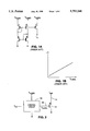
- FIG. 1A Such a typical current mirror is shown in FIG. 1A with the variation in current as a function of the supply voltage shown in FIG. 1B.
- a current source which provides a stable current despite variations in the supply voltage.
- a current source it is desirable for a current source to have an output current which can be controlled in a predictable manner to change as a function of changing supply voltage.
- a current source in which the output current can be increased or decreased as a function of a reference voltage applied to the current source.
- the present invention provides a stable current source which can operate over a wide supply voltage range, and which can increase or decrease current as a function of the supply voltage or a user supplied reference voltage.
- a current source is provided which is powered from a supply voltage and includes a source of current that provides a predetermined amount of current.
- a first semiconductor device is coupled to receive current from the source of current and provides an output voltage which has a selected relationship to the magnitude of current received from the source of current.
- a plurality of controllable current paths are connected to receive the current from the output from the source of current, and each of the plurality of controllable current paths is constructed to accommodate a selected amount of current when activated.
- a voltage sensing circuit is coupled to receive a control voltage and activates ones of the controllable current paths as a function of changes in the magnitude of the control voltage.
- a second semiconductor device is coupled to receive the output voltage from the first semiconductor device and provides an output current having a selected relationship to the magnitude of output voltage received from the first device. In this manner, as different numbers of controllable current paths are activated by the voltage sensing circuit, more or less current is drawn away from the first semiconductor device and thereby affects the amount of current which flows into the first semiconductor device. This results in a change in output voltage developed by the first semiconductor device and applied to the second semiconductor device. In turn, the output current supplied by the second semiconductor device will change as a function of the change in output voltage it receives from the first device.
- the voltage sensing circuit can be coupled to the supply voltage, or to a reference voltage supplied by the user.
- two voltage sensing circuits can be used, one coupled to the supply voltage, and the other coupled to receive a control or reference voltage from the user.
- FIG. 1A is a simplified schematic diagram of a conventional current mirror.
- FIG. 1B is a plot of the variation of current provided by the current mirror of FIG. 1A as a function of the supply voltage.
- FIG. 2 is a high-level functional block diagram of one embodiment of the present invention.
- FIG. 3 is a simplified schematic diagram of an embodiment of the present invention in which the output current is controlled as a function of the supply voltage.
- FIG. 4 is a simplified schematic diagram of a further embodiment of the present invention in which the output current is controlled as a function of the supply voltage as well a reference voltage.
- FIG. 5 is simplified plot of the different output current variations as a function of supply voltage which can be obtained in accordance with the present invention.
- FIG. 6 is a still further embodiment of the present invention in which the output current can be controlled to increase as the supply voltage increases.
- the present invention includes an output device 12 which provides an output current at an output terminal 14 as a function of a control voltage supplied to a control terminal 16.
- output device 12 is an MOS transistor.
- the control circuit 18 which provides the control voltage to output device 12 is powered from the supply voltage, V supply , and can also be controlled by a reference voltage V ref .
- V control supplied from control circuit 18 varies in a predetermined manner as V supply and V ref vary.
- control circuit 18 includes a conventional current mirror 20, which supplies current to a diode-connected transistor 22. Connected to the diode-connected transistor 22 are a set of controllable current paths 24. Each of these controllable current paths is controlled by voltages supplied from a voltage sensing circuit 26.
- current i m from current mirror 20, is caused to flow into diode-connected transistor 22. This induces a voltage on line 16 which is applied to the control gate of transistor 12 to control the output current i out flowing through transistor 12.
- Each of the current paths in the set of current paths 24 is controlled by a voltage from the voltage sensing circuit 26. More particularly, voltage sensing circuit 26 is formed of a ladder of diode-connected transistors. It is to be noted that each of the controllable current paths 30 is connected to a different node on the ladder, so that each of the paths will be activated depending upon the magnitude of the supply voltage applied at the top of the ladder. For example, the controllable current path controlled by the voltage at node 32 will be activated when V supply is 3 thresholds, V T , above ground. In turn, the controllable current path 30 which is controlled from node 34 of voltage sensing circuit 26 will be activated when V supply is 4 thresholds voltages above ground.
- the amount of current drawn away from diode-connected transistor 22 can be controlled as a function of the magnitude of supply voltage V supply . It is further to be understood that the threshold voltages of the diode-connected transistors in the voltage sensing circuit 26 can be made to be different (for example by varying the physical size of the transistors) from the threshold voltages of the transistors in controllable paths 30 so that further variations in control can be obtained.
- each of the controllable current paths 30 is preferably constructed of a pair of series connected transistors, each pair of which is connected in parallel with diode-connected transistor 22.
- One of the pair of transistors has its drain connected to the drain of diode-connected transistor 22 and its gate connected to the gate of the diode-connected transistor 22.
- the second transistor has its drain connected to the source of the first transistor, a source connected to ground, and a control gate which receives a corresponding control voltage from the voltage sensing circuit 26.
- the first transistor 36 can be sized to draw a predetermined amount of current from current mirror 20 as a function of the gate-source voltage induced across transistor 22. For example, for a given gate-source voltage across diode-connected transistor 22, transistor 36 can be sized to draw 1/10 of the current flowing through transistor 22 for the same gate-source voltage supplied across diode-connected transistor 22.
- the circuitry illustrated is similar to that in FIG. 3, except that a second set of controllable current paths 40, and a second voltage sensing circuit 42, have been added.
- the voltage sensing circuit 42 is constructed similarly to voltage sensing circuit 26, but is coupled to a reference voltage which can be supplied by the user. Further, it is to be noted that the control voltages are taken from different nodes of the voltage sensing circuit 42 when compared to that of sensing circuit 26. This means that a different magnitude of voltage at V ref will be required to activate different ones of the second set of controllable current paths 40.
- the amount of current which is permitted to flow into diode-connected transistor 22 can be controlled as desired.
- the transistors in controllable current paths 30 can be sized, and the control voltages from voltage sensing circuit 26 selected, to provide an output current which does not vary appreciable as the supply voltage level varies. More particularly, the controllable current paths would be controlled to draw less current as the magnitude of the voltage supply decreases, and the rate at which such decrease occurs is selected to offset the rate at which current mirror 20 decreases the magnitude of current i m with decreasing supply voltage. In this manner, the current flowing through diode-connected transistor 22 will remain substantially the same even though the supply voltage is decreasing.
- the transistor in the controllable current paths 20 can be selected so that the amount of current which is permitted to flow into diode-connected transistor 22 is higher at low supply voltages than it is at higher supply voltages. Referring to FIG. 5, this latter condition is illustrated by graph 44. Similarly, the situation in which the current flow into diode-connected transistor 22 is kept constant over the supply variation, is illustrated in FIG. 5 by graph 46.
- FIG. 6 an embodiment of the present invention is shown in which the output current i out increases with increasing supply voltage.
- the difference between FIGS. 3 and 4 versus FIG. 6 is that in the controllable current paths of the former, N-channel transistors are used for both 36 and 38.
- N-channel transistors are used for transistor 36, but a P-channel transistor 48 is used in place of the N-channel transistor 38.
Landscapes
- Engineering & Computer Science (AREA)
- Physics & Mathematics (AREA)
- Microelectronics & Electronic Packaging (AREA)
- Radar, Positioning & Navigation (AREA)
- Electromagnetism (AREA)
- General Physics & Mathematics (AREA)
- Nonlinear Science (AREA)
- Automation & Control Theory (AREA)
- Power Engineering (AREA)
- Computer Hardware Design (AREA)
- Computing Systems (AREA)
- General Engineering & Computer Science (AREA)
- Mathematical Physics (AREA)
- Control Of Electrical Variables (AREA)
- Electronic Switches (AREA)
Priority Applications (8)
| Application Number | Priority Date | Filing Date | Title |
|---|---|---|---|
| US08/690,008 US5793248A (en) | 1996-07-31 | 1996-07-31 | Voltage controlled variable current reference |
| CN97198322A CN1231780A (zh) | 1996-07-31 | 1997-07-24 | 受电压控制的可变电流基准 |
| CA002261733A CA2261733A1 (fr) | 1996-07-31 | 1997-07-24 | Reference de courant variable commande en tension |
| PCT/US1997/012984 WO1998005125A1 (fr) | 1996-07-31 | 1997-07-24 | Reference de courant variable commande en tension |
| JP10508973A JP2001500997A (ja) | 1996-07-31 | 1997-07-24 | 電圧制御された可変参照電流 |
| AU38924/97A AU3892497A (en) | 1996-07-31 | 1997-07-24 | Voltage controlled variable current reference |
| EP97936194A EP0916187A4 (fr) | 1996-07-31 | 1997-07-24 | Reference de courant variable commande en tension |
| KR10-1999-7000736A KR100414596B1 (ko) | 1996-07-31 | 1997-07-24 | 전압 제어된 가변 전류 레퍼런스 |
Applications Claiming Priority (1)
| Application Number | Priority Date | Filing Date | Title |
|---|---|---|---|
| US08/690,008 US5793248A (en) | 1996-07-31 | 1996-07-31 | Voltage controlled variable current reference |
Publications (1)
| Publication Number | Publication Date |
|---|---|
| US5793248A true US5793248A (en) | 1998-08-11 |
Family
ID=24770727
Family Applications (1)
| Application Number | Title | Priority Date | Filing Date |
|---|---|---|---|
| US08/690,008 Expired - Lifetime US5793248A (en) | 1996-07-31 | 1996-07-31 | Voltage controlled variable current reference |
Country Status (8)
| Country | Link |
|---|---|
| US (1) | US5793248A (fr) |
| EP (1) | EP0916187A4 (fr) |
| JP (1) | JP2001500997A (fr) |
| KR (1) | KR100414596B1 (fr) |
| CN (1) | CN1231780A (fr) |
| AU (1) | AU3892497A (fr) |
| CA (1) | CA2261733A1 (fr) |
| WO (1) | WO1998005125A1 (fr) |
Cited By (15)
| Publication number | Priority date | Publication date | Assignee | Title |
|---|---|---|---|---|
| US6445170B1 (en) | 2000-10-24 | 2002-09-03 | Intel Corporation | Current source with internal variable resistance and control loop for reduced process sensitivity |
| US6448811B1 (en) * | 2001-04-02 | 2002-09-10 | Intel Corporation | Integrated circuit current reference |
| US6529037B1 (en) | 2001-09-13 | 2003-03-04 | Intel Corporation | Voltage mode bidirectional port with data channel used for synchronization |
| US20030122586A1 (en) * | 2001-04-16 | 2003-07-03 | Intel Corporation | Differential cascode current mode driver |
| US6597198B2 (en) | 2001-10-05 | 2003-07-22 | Intel Corporation | Current mode bidirectional port with data channel used for synchronization |
| US20040080362A1 (en) * | 2001-12-19 | 2004-04-29 | Narendra Siva G. | Current reference apparatus and systems |
| US20040080338A1 (en) * | 2001-06-28 | 2004-04-29 | Haycock Matthew B. | Bidirectional port with clock channel used for synchronization |
| US20050003764A1 (en) * | 2003-06-18 | 2005-01-06 | Intel Corporation | Current control circuit |
| US20050248371A1 (en) * | 2004-05-06 | 2005-11-10 | Hack-Soo Oh | Current to voltage amplifier |
| US20060033557A1 (en) * | 2002-05-21 | 2006-02-16 | Christofer Toumazou | Reference circuit |
| US20060055454A1 (en) * | 2004-09-14 | 2006-03-16 | Dialog Semiconductor Gmbh | Dynamic transconductance boosting technique for current mirrors |
| US7222208B1 (en) | 2000-08-23 | 2007-05-22 | Intel Corporation | Simultaneous bidirectional port with synchronization circuit to synchronize the port with another port |
| US20090160539A1 (en) * | 2007-12-20 | 2009-06-25 | Airoha Technology Corp. | Voltage reference circuit |
| CN102622957A (zh) * | 2011-02-01 | 2012-08-01 | 北京大学 | 基于恒定栅压线性区mosfet的多通道led恒流源驱动 |
| CN101557669B (zh) * | 2009-03-11 | 2012-10-03 | 深圳市民展科技开发有限公司 | 一种高精度可控电流源 |
Families Citing this family (3)
| Publication number | Priority date | Publication date | Assignee | Title |
|---|---|---|---|---|
| US5793248A (en) * | 1996-07-31 | 1998-08-11 | Exel Microelectronics, Inc. | Voltage controlled variable current reference |
| GB9920080D0 (en) * | 1999-08-24 | 1999-10-27 | Sgs Thomson Microelectronics | Current reference circuit |
| CN101694963B (zh) * | 2009-09-22 | 2013-09-18 | 美芯晟科技(北京)有限公司 | 高精度低电压的电压电流转换电路 |
Citations (3)
| Publication number | Priority date | Publication date | Assignee | Title |
|---|---|---|---|---|
| US4864162A (en) * | 1988-05-10 | 1989-09-05 | Grumman Aerospace Corporation | Voltage variable FET resistor with chosen resistance-voltage relationship |
| US5457407A (en) * | 1994-07-06 | 1995-10-10 | Sony Electronics Inc. | Binary weighted reference circuit for a variable impedance output buffer |
| US5583464A (en) * | 1994-05-13 | 1996-12-10 | Thinking Machines Corporation | Resistor circuit for integrated circuit chip using insulated field effect transistors |
Family Cites Families (6)
| Publication number | Priority date | Publication date | Assignee | Title |
|---|---|---|---|---|
| JPS5672350A (en) * | 1979-11-19 | 1981-06-16 | Advantest Corp | Variable current source |
| JPS5750139A (en) * | 1980-09-10 | 1982-03-24 | Toshiba Corp | Hysteresis circuit |
| US4608530A (en) * | 1984-11-09 | 1986-08-26 | Harris Corporation | Programmable current mirror |
| JPH06343022A (ja) * | 1993-06-01 | 1994-12-13 | Fujitsu Ltd | 電圧制御発振回路 |
| US5483151A (en) * | 1994-09-27 | 1996-01-09 | Mitsubishi Denki Kabushiki Kaisha | Variable current source for variably controlling an output current in accordance with a control voltage |
| US5793248A (en) * | 1996-07-31 | 1998-08-11 | Exel Microelectronics, Inc. | Voltage controlled variable current reference |
-
1996
- 1996-07-31 US US08/690,008 patent/US5793248A/en not_active Expired - Lifetime
-
1997
- 1997-07-24 CA CA002261733A patent/CA2261733A1/fr not_active Abandoned
- 1997-07-24 CN CN97198322A patent/CN1231780A/zh active Pending
- 1997-07-24 KR KR10-1999-7000736A patent/KR100414596B1/ko not_active Expired - Fee Related
- 1997-07-24 EP EP97936194A patent/EP0916187A4/fr not_active Withdrawn
- 1997-07-24 WO PCT/US1997/012984 patent/WO1998005125A1/fr not_active Ceased
- 1997-07-24 JP JP10508973A patent/JP2001500997A/ja active Pending
- 1997-07-24 AU AU38924/97A patent/AU3892497A/en not_active Abandoned
Patent Citations (4)
| Publication number | Priority date | Publication date | Assignee | Title |
|---|---|---|---|---|
| US4864162A (en) * | 1988-05-10 | 1989-09-05 | Grumman Aerospace Corporation | Voltage variable FET resistor with chosen resistance-voltage relationship |
| US4864162B1 (fr) * | 1988-05-10 | 1992-10-13 | Grumman Aerospace Corp | |
| US5583464A (en) * | 1994-05-13 | 1996-12-10 | Thinking Machines Corporation | Resistor circuit for integrated circuit chip using insulated field effect transistors |
| US5457407A (en) * | 1994-07-06 | 1995-10-10 | Sony Electronics Inc. | Binary weighted reference circuit for a variable impedance output buffer |
Cited By (21)
| Publication number | Priority date | Publication date | Assignee | Title |
|---|---|---|---|---|
| US7222208B1 (en) | 2000-08-23 | 2007-05-22 | Intel Corporation | Simultaneous bidirectional port with synchronization circuit to synchronize the port with another port |
| US6445170B1 (en) | 2000-10-24 | 2002-09-03 | Intel Corporation | Current source with internal variable resistance and control loop for reduced process sensitivity |
| US6448811B1 (en) * | 2001-04-02 | 2002-09-10 | Intel Corporation | Integrated circuit current reference |
| US20030122586A1 (en) * | 2001-04-16 | 2003-07-03 | Intel Corporation | Differential cascode current mode driver |
| US6774678B2 (en) | 2001-04-16 | 2004-08-10 | Intel Corporation | Differential cascode current mode driver |
| US20040080338A1 (en) * | 2001-06-28 | 2004-04-29 | Haycock Matthew B. | Bidirectional port with clock channel used for synchronization |
| US6803790B2 (en) | 2001-06-28 | 2004-10-12 | Intel Corporation | Bidirectional port with clock channel used for synchronization |
| US6529037B1 (en) | 2001-09-13 | 2003-03-04 | Intel Corporation | Voltage mode bidirectional port with data channel used for synchronization |
| US6597198B2 (en) | 2001-10-05 | 2003-07-22 | Intel Corporation | Current mode bidirectional port with data channel used for synchronization |
| US20040080362A1 (en) * | 2001-12-19 | 2004-04-29 | Narendra Siva G. | Current reference apparatus and systems |
| US6975005B2 (en) * | 2001-12-19 | 2005-12-13 | Intel Corporation | Current reference apparatus and systems |
| US20060033557A1 (en) * | 2002-05-21 | 2006-02-16 | Christofer Toumazou | Reference circuit |
| US7242241B2 (en) * | 2002-05-21 | 2007-07-10 | Dna Electronics Limited | Reference circuit |
| US20050003764A1 (en) * | 2003-06-18 | 2005-01-06 | Intel Corporation | Current control circuit |
| US20050248371A1 (en) * | 2004-05-06 | 2005-11-10 | Hack-Soo Oh | Current to voltage amplifier |
| US20060055454A1 (en) * | 2004-09-14 | 2006-03-16 | Dialog Semiconductor Gmbh | Dynamic transconductance boosting technique for current mirrors |
| US7119605B2 (en) * | 2004-09-14 | 2006-10-10 | Dialog Semiconductor Gmbh | Dynamic transconductance boosting technique for current mirrors |
| US20090160539A1 (en) * | 2007-12-20 | 2009-06-25 | Airoha Technology Corp. | Voltage reference circuit |
| CN101557669B (zh) * | 2009-03-11 | 2012-10-03 | 深圳市民展科技开发有限公司 | 一种高精度可控电流源 |
| CN102622957A (zh) * | 2011-02-01 | 2012-08-01 | 北京大学 | 基于恒定栅压线性区mosfet的多通道led恒流源驱动 |
| CN102622957B (zh) * | 2011-02-01 | 2014-07-02 | 北京大学 | 基于恒定栅压线性区mosfet的多通道led恒流源驱动 |
Also Published As
| Publication number | Publication date |
|---|---|
| KR20000029660A (ko) | 2000-05-25 |
| AU3892497A (en) | 1998-02-20 |
| KR100414596B1 (ko) | 2004-01-13 |
| WO1998005125A1 (fr) | 1998-02-05 |
| JP2001500997A (ja) | 2001-01-23 |
| EP0916187A4 (fr) | 1999-12-29 |
| CN1231780A (zh) | 1999-10-13 |
| CA2261733A1 (fr) | 1998-02-05 |
| EP0916187A1 (fr) | 1999-05-19 |
Similar Documents
| Publication | Publication Date | Title |
|---|---|---|
| US5793248A (en) | Voltage controlled variable current reference | |
| EP0000844B1 (fr) | Circuit à semi-conducteur pour la commande d'un dispositif commandé. | |
| WO1998005125A9 (fr) | Reference de courant variable commande en tension | |
| KR101465598B1 (ko) | 기준 전압 발생 장치 및 방법 | |
| US6998902B2 (en) | Bandgap reference voltage circuit | |
| KR100393226B1 (ko) | 온도변화에 따라 내부 기준전압 값을 조절할 수 있는 내부기준전압 생성회로 및 이를 구비하는 내부 공급전압생성회로 | |
| US7602162B2 (en) | Voltage regulator with over-current protection | |
| US5990671A (en) | Constant power voltage generator with current mirror amplifier optimized by level shifters | |
| US4004158A (en) | Keyed comparator | |
| US5804958A (en) | Self-referenced control circuit | |
| US6989692B1 (en) | Substrate-sensing voltage sensor for voltage comparator with voltage-to-current converters for both reference and input voltages | |
| EP0121793B1 (fr) | Circuits CMOS comportant un régulateur de tension adapté à un paramètre | |
| JP2002237731A (ja) | 電圧制御型カレントソース回路及び電流制御方法 | |
| KR19980043784A (ko) | 외부전압에 둔감한 백바이어스전압 레벨 감지기 | |
| US20060125460A1 (en) | Reference current generator | |
| US6411159B1 (en) | Circuit for controlling current levels in differential logic circuitry | |
| US7091712B2 (en) | Circuit for performing voltage regulation | |
| US5532617A (en) | CMOS input with temperature and VCC compensated threshold | |
| US20020175663A1 (en) | Reference voltage generator tolerant to temperature variations | |
| KR0172436B1 (ko) | 반도체 장치의 기준전압 발생회로 | |
| US5694073A (en) | Temperature and supply-voltage sensing circuit | |
| KR920004587B1 (ko) | 메모리장치의 기준전압 안정화회로 | |
| KR20040024789A (ko) | 안정된 내부 전압을 발생하는 내부전압 발생기 | |
| US7312601B2 (en) | Start-up circuit for a current generator | |
| US6597237B2 (en) | Reference potential generator |
Legal Events
| Date | Code | Title | Description |
|---|---|---|---|
| AS | Assignment |
Owner name: EXEI MICROELECTRONICS, INC, CALIFORNIA Free format text: ASSIGNMENT OF ASSIGNORS INTEREST;ASSIGNORS:LEE, LAN;AWSARE, SALEEL;REEL/FRAME:008141/0948 Effective date: 19960729 |
|
| STCF | Information on status: patent grant |
Free format text: PATENTED CASE |
|
| FEPP | Fee payment procedure |
Free format text: PAYOR NUMBER ASSIGNED (ORIGINAL EVENT CODE: ASPN); ENTITY STATUS OF PATENT OWNER: LARGE ENTITY |
|
| AS | Assignment |
Owner name: ROHM U.S.A., INC., CALIFORNIA Free format text: ASSIGNMENT OF ASSIGNORS INTEREST;ASSIGNOR:EXEL MICROELECTRONICS, INC.;REEL/FRAME:009883/0477 Effective date: 19990330 |
|
| AS | Assignment |
Owner name: ROHM AMERICAS, INC., CALIFORNIA Free format text: ASSIGNMENT OF ASSIGNORS INTEREST;ASSIGNOR:ROHM U.S.A., INC.;REEL/FRAME:012090/0509 Effective date: 20010517 |
|
| AS | Assignment |
Owner name: ROHM U.S.A., INC., CALIFORNIA Free format text: CHANGE OF NAME;ASSIGNOR:ROHM AMERICAS, INC.;REEL/FRAME:012103/0199 Effective date: 20010607 |
|
| FPAY | Fee payment |
Year of fee payment: 4 |
|
| FPAY | Fee payment |
Year of fee payment: 8 |
|
| FPAY | Fee payment |
Year of fee payment: 12 |