US5796979A - Data processing system having demand based write through cache with enforced ordering - Google Patents
Data processing system having demand based write through cache with enforced ordering Download PDFInfo
- Publication number
- US5796979A US5796979A US08/730,994 US73099496A US5796979A US 5796979 A US5796979 A US 5796979A US 73099496 A US73099496 A US 73099496A US 5796979 A US5796979 A US 5796979A
- Authority
- US
- United States
- Prior art keywords
- cache
- write
- data
- memory
- system memory
- Prior art date
- Legal status (The legal status is an assumption and is not a legal conclusion. Google has not performed a legal analysis and makes no representation as to the accuracy of the status listed.)
- Expired - Fee Related
Links
Images


Classifications
-
- G—PHYSICS
- G06—COMPUTING OR CALCULATING; COUNTING
- G06F—ELECTRIC DIGITAL DATA PROCESSING
- G06F13/00—Interconnection of, or transfer of information or other signals between, memories, input/output devices or central processing units
- G06F13/14—Handling requests for interconnection or transfer
-
- G—PHYSICS
- G06—COMPUTING OR CALCULATING; COUNTING
- G06F—ELECTRIC DIGITAL DATA PROCESSING
- G06F12/00—Accessing, addressing or allocating within memory systems or architectures
- G06F12/02—Addressing or allocation; Relocation
- G06F12/08—Addressing or allocation; Relocation in hierarchically structured memory systems, e.g. virtual memory systems
- G06F12/0802—Addressing of a memory level in which the access to the desired data or data block requires associative addressing means, e.g. caches
- G06F12/0866—Addressing of a memory level in which the access to the desired data or data block requires associative addressing means, e.g. caches for peripheral storage systems, e.g. disk cache
-
- G—PHYSICS
- G06—COMPUTING OR CALCULATING; COUNTING
- G06F—ELECTRIC DIGITAL DATA PROCESSING
- G06F12/00—Accessing, addressing or allocating within memory systems or architectures
- G06F12/02—Addressing or allocation; Relocation
- G06F12/08—Addressing or allocation; Relocation in hierarchically structured memory systems, e.g. virtual memory systems
- G06F12/0802—Addressing of a memory level in which the access to the desired data or data block requires associative addressing means, e.g. caches
- G06F12/0806—Multiuser, multiprocessor or multiprocessing cache systems
- G06F12/0815—Cache consistency protocols
-
- G—PHYSICS
- G06—COMPUTING OR CALCULATING; COUNTING
- G06F—ELECTRIC DIGITAL DATA PROCESSING
- G06F12/00—Accessing, addressing or allocating within memory systems or architectures
- G06F12/02—Addressing or allocation; Relocation
- G06F12/08—Addressing or allocation; Relocation in hierarchically structured memory systems, e.g. virtual memory systems
- G06F12/0802—Addressing of a memory level in which the access to the desired data or data block requires associative addressing means, e.g. caches
- G06F12/0806—Multiuser, multiprocessor or multiprocessing cache systems
- G06F12/0815—Cache consistency protocols
- G06F12/0831—Cache consistency protocols using a bus scheme, e.g. with bus monitoring or watching means
- G06F12/0835—Cache consistency protocols using a bus scheme, e.g. with bus monitoring or watching means for main memory peripheral accesses (e.g. I/O or DMA)
-
- G—PHYSICS
- G06—COMPUTING OR CALCULATING; COUNTING
- G06F—ELECTRIC DIGITAL DATA PROCESSING
- G06F2212/00—Indexing scheme relating to accessing, addressing or allocation within memory systems or architectures
- G06F2212/30—Providing cache or TLB in specific location of a processing system
- G06F2212/303—In peripheral interface, e.g. I/O adapter or channel
Definitions
- the present invention relates to data processing systems, and more particularly to data processing systems having one or more processors, a system storage, a system bus and one or more input/output channel controllers ("IOCC") and allowing direct memory access (DMA) from I/O channel controllers to system memory.
- IOCC input/output channel controllers
- DMA direct memory access
- Direct memory access is almost as old as the computer industry. It was first developed by Carl Christiansen, et al. for the IBM 705 computer system in 1956. The Christiansen, et al. U.S. Pat. No. 3,812,475 showed the basic DMA techniques employed in a Von Neumann computer architecture system.
- DMA techniques for systems including caches and write through caches are generally well-known in the art.
- a typical write through cache forwards each cache modification with an appropriate system memory modification.
- an equivalent multiple of system memory write operations occur.
- Write through caches are typically used in computer systems to reduce cache controller complexity and minimize cache and memory data inconsistencies.
- Processors, IOCCs and I/O devices commonly use traditional write through caches in order to obtain these benefits.
- a data processing system includes a processor, a system memory, one or more input/output channel controllers (IOCC), and a system bus connecting the processor, the memory and the IOCCs together for communicating instructions, address and data between the various elements of a system.
- the IOCC includes a paged cache storage having a number of lines wherein each line of the page may be, for example, 32 bytes.
- Each page in the cache also has several attribute bits for that page including the so called WIM and attribute bits.
- the W bit is for controlling write through operations; the I bit controls cache inhibit; and the M bit controls memory coherency. Since the IOCC is unaware of these page table attribute bits for the cache lines being DMAed to system memory, IOCC must maintain memory consistency and cache coherency without sacrificing performance.
- the method and apparatus according to the present invention provides high performance write through caches by gathering write data and performing block writes to system memory based on predetermined demand criteria.
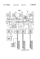
- FIG. 1 is a system block diagram of a data processing system embodying the present invention.
- FIG. 2 is a block diagram of a demand based write through cache in accordance with the present invention.
- FIG. 3 is a flow chart describing the operation of the demand based write through cache technique in accordance with the present invention.
- Multiprocessor system 100 includes a number of processing units 102, 104, 106 operatively connected to a system bus 108. Also connected to the system bus 108 is a memory controller 110, which controls access to system memory 112, and I/O channel controllers 114, 116, and 118. Additionally, a high performance I/O device 120 may be connected to the system bus 108.
- system controller 130 which communicates with each unit connected to the system bus 108 by point to point lines such as 132 to processor 102, 134 to processor 104, 136 to processor 106, 140 to memory controller 110, 144 to I/O channel controller 114, 146 to I/O channel controller 116, 148 to I/O channel controller 118, and 150 to high performance I/O device 120. Requests and grants of bus access are all controlled by system controller 130.
- I/O channel controller 114 controls and is connected to system I/O subsystem and native I/O subsystem 160.
- Each processor unit 102, 104, 106 may include a processor and a cache storage device.
- Cache 200 is organized as a 128 byte circular cache having two 64-byte cache lines wherein the cache is divided into four 32-byte sectors 202, 204, 206 and 208. From the system bus, this cache structure allows the IOCC, for example, IOCC 114 (see FIG. 1) to efficiently support systems with either 32-byte or 64-byte coherency requirements. Due to the coherency requirements of the system bus, there are many cases in which DMA write data by the IOCC is retried on the system bus for lengthy periods of time.
- the DMA write cache organization provides a relatively efficient means of isolating system bus traffic from I/O bus transfers, thus improving I/O bus throughput and bandwidth.
- IOCC 114 By organizing cache 200 as four 32-byte sectors, coupled with the circular structure of cache 200, IOCC 114 performs heavy pipelining of sequential write data thus allowing the I/O bus devices to sustain a high data rate via the I/O bus interface controller 250.
- the WIM attribute bits associated with system memory pages are shown in the following table with the meaning of each combination of WIM bits.
- WIM bits are managed by the operating system software and are accessed by processor 102, etc. (and I/O devices) to determine the cache attributes associated with each system memory page. Unlike processor 102, most IOCCs 114, etc. and I/O devices are unaware of the value of the WIM attribute bits. Thus, during I/O DMA write operations to system memory 112, IOCC 114 must support the 101 code in order to avoid I/O cache and memory data inconsistencies. This then allows IOCC 114 to extend the 101 code and support a demand based write through cache. In some systems, IOCC 114 is aware of the WIM attribute bits and supports demand based write through cache if the WIM bits equal the 101 code.
- the operation of the demand based write through cache will be described. If a demand based write through cache operation is to be performed, the WIM bits will be "101".
- the process tests for an I/O DMA write operation step 310.
- the process loops until the write operation is received.
- the process then proceeds to write the data in the IOCC cache at step 320.
- the process loops until all data is written into the IOCC cache (step 320) at which time the process then moves to step 330, which is the hold write operation to system step.
- the hold write operation to system memory at 330 is employed to cause the process to wait until one of several events occurs and then allow a block write of the held modified data to system memory.
- Test is made at step 340 to determine whether the I/O device has:
- step 340 If none of these events have occurred, the process loops back to step 320 to allow additional data to be written into the cache of the IOCC (i.e., 114). If any of the events set forth in step 340 have occurred, a block write of modified data to system memory 112 is then performed at step 350.
- Another feature of the present invention relates to maintaining write ordering to system memory.
- coherency mechanisms such as cache level snooping, retry and push protocols have been used to maintain write ordering between cache and system memory. (Snooping, retry, and push protocols are well known in the art).
- the apparatus and method according to the present invention having a demand based write through cache can significantly improve system performance and reduce design complexity by providing a byte level write ordering rather than cache level snooping, retry or push.
- Byte level ordering is achieved in a demand based write through cache by adding another condition to the demand criteria. This condition checks to determine if the I/O bus master ever writes "backwards" within the same cache line. That is, if address B is less than address A in the same line, then the write operation for B is held off until the demand based write through cache data is forwarded to system memory.
- I/O cache coherency and write data ordering are achieved without the IOCC ever having to snoop, retry or push the DMA write data.
Landscapes
- Engineering & Computer Science (AREA)
- Theoretical Computer Science (AREA)
- Physics & Mathematics (AREA)
- General Engineering & Computer Science (AREA)
- General Physics & Mathematics (AREA)
- Memory System Of A Hierarchy Structure (AREA)
Priority Applications (1)
| Application Number | Priority Date | Filing Date | Title |
|---|---|---|---|
| US08/730,994 US5796979A (en) | 1994-10-03 | 1996-10-16 | Data processing system having demand based write through cache with enforced ordering |
Applications Claiming Priority (2)
| Application Number | Priority Date | Filing Date | Title |
|---|---|---|---|
| US31697994A | 1994-10-03 | 1994-10-03 | |
| US08/730,994 US5796979A (en) | 1994-10-03 | 1996-10-16 | Data processing system having demand based write through cache with enforced ordering |
Related Parent Applications (1)
| Application Number | Title | Priority Date | Filing Date |
|---|---|---|---|
| US31697994A Continuation | 1994-10-03 | 1994-10-03 |
Publications (1)
| Publication Number | Publication Date |
|---|---|
| US5796979A true US5796979A (en) | 1998-08-18 |
Family
ID=23231576
Family Applications (1)
| Application Number | Title | Priority Date | Filing Date |
|---|---|---|---|
| US08/730,994 Expired - Fee Related US5796979A (en) | 1994-10-03 | 1996-10-16 | Data processing system having demand based write through cache with enforced ordering |
Country Status (4)
| Country | Link |
|---|---|
| US (1) | US5796979A (de) |
| EP (1) | EP0706134A3 (de) |
| JP (1) | JP3266470B2 (de) |
| KR (1) | KR0175983B1 (de) |
Cited By (13)
| Publication number | Priority date | Publication date | Assignee | Title |
|---|---|---|---|---|
| US6108721A (en) * | 1998-06-29 | 2000-08-22 | Hewlett-Packard Company | Method and apparatus for ensuring data consistency between an i/o channel and a processor |
| US20030018690A1 (en) * | 2001-03-12 | 2003-01-23 | James Kulp | Digital data processing apparatus and methods with dynamically configurable application execution on accelerated resources |
| US6658537B2 (en) * | 1997-06-09 | 2003-12-02 | 3Com Corporation | DMA driven processor cache |
| US6728869B1 (en) * | 2000-04-21 | 2004-04-27 | Ati International Srl | Method and apparatus for memory latency avoidance in a processing system |
| US6785759B1 (en) | 2000-05-10 | 2004-08-31 | International Business Machines Corporation | System and method for sharing I/O address translation caching across multiple host bridges |
| US20050049929A1 (en) * | 2003-08-29 | 2005-03-03 | International Business Machines Corporation | Method and apparatus for trading digital items in a network data processing system |
| US20050049972A1 (en) * | 2003-08-29 | 2005-03-03 | International Business Machines Corporation | Method and apparatus for temporary ownership of digital items in a network data processing system |
| US20050050170A1 (en) * | 2003-08-29 | 2005-03-03 | International Business Machines Corporation | Method and apparatus for securely conducting digital property trade |
| US20060174062A1 (en) * | 2005-02-02 | 2006-08-03 | Bockhaus John W | Method and system for cache utilization by limiting number of pending cache line requests |
| US20060179175A1 (en) * | 2005-02-02 | 2006-08-10 | Bockhaus John W | Method and system for cache utilization by limiting prefetch requests |
| US20060179173A1 (en) * | 2005-02-02 | 2006-08-10 | Bockhaus John W | Method and system for cache utilization by prefetching for multiple DMA reads |
| US20060179174A1 (en) * | 2005-02-02 | 2006-08-10 | Bockhaus John W | Method and system for preventing cache lines from being flushed until data stored therein is used |
| US20100235581A1 (en) * | 2009-03-10 | 2010-09-16 | Anderson Eric A | Cooperative Caching Technique |
Families Citing this family (2)
| Publication number | Priority date | Publication date | Assignee | Title |
|---|---|---|---|---|
| US6249845B1 (en) | 1998-08-19 | 2001-06-19 | International Business Machines Corporation | Method for supporting cache control instructions within a coherency granule |
| US7991965B2 (en) * | 2006-02-07 | 2011-08-02 | Intel Corporation | Technique for using memory attributes |
Citations (6)
| Publication number | Priority date | Publication date | Assignee | Title |
|---|---|---|---|---|
| US3812475A (en) * | 1957-12-26 | 1974-05-21 | Ibm | Data synchronizer |
| US3967247A (en) * | 1974-11-11 | 1976-06-29 | Sperry Rand Corporation | Storage interface unit |
| US4394733A (en) * | 1980-11-14 | 1983-07-19 | Sperry Corporation | Cache/disk subsystem |
| US4713755A (en) * | 1985-06-28 | 1987-12-15 | Hewlett-Packard Company | Cache memory consistency control with explicit software instructions |
| WO1990003002A1 (en) * | 1988-09-02 | 1990-03-22 | Aris Corporation | Coherent cache structures and methods |
| WO1994008296A1 (en) * | 1992-10-02 | 1994-04-14 | Compaq Computer Corporation | Double buffering operations between the memory bus and the expansion bus of a computer system |
-
1995
- 1995-09-14 JP JP23640295A patent/JP3266470B2/ja not_active Expired - Fee Related
- 1995-09-22 EP EP95480140A patent/EP0706134A3/de not_active Withdrawn
- 1995-09-30 KR KR1019950033599A patent/KR0175983B1/ko not_active Expired - Fee Related
-
1996
- 1996-10-16 US US08/730,994 patent/US5796979A/en not_active Expired - Fee Related
Patent Citations (6)
| Publication number | Priority date | Publication date | Assignee | Title |
|---|---|---|---|---|
| US3812475A (en) * | 1957-12-26 | 1974-05-21 | Ibm | Data synchronizer |
| US3967247A (en) * | 1974-11-11 | 1976-06-29 | Sperry Rand Corporation | Storage interface unit |
| US4394733A (en) * | 1980-11-14 | 1983-07-19 | Sperry Corporation | Cache/disk subsystem |
| US4713755A (en) * | 1985-06-28 | 1987-12-15 | Hewlett-Packard Company | Cache memory consistency control with explicit software instructions |
| WO1990003002A1 (en) * | 1988-09-02 | 1990-03-22 | Aris Corporation | Coherent cache structures and methods |
| WO1994008296A1 (en) * | 1992-10-02 | 1994-04-14 | Compaq Computer Corporation | Double buffering operations between the memory bus and the expansion bus of a computer system |
Cited By (18)
| Publication number | Priority date | Publication date | Assignee | Title |
|---|---|---|---|---|
| US6658537B2 (en) * | 1997-06-09 | 2003-12-02 | 3Com Corporation | DMA driven processor cache |
| US6108721A (en) * | 1998-06-29 | 2000-08-22 | Hewlett-Packard Company | Method and apparatus for ensuring data consistency between an i/o channel and a processor |
| US6728869B1 (en) * | 2000-04-21 | 2004-04-27 | Ati International Srl | Method and apparatus for memory latency avoidance in a processing system |
| US6785759B1 (en) | 2000-05-10 | 2004-08-31 | International Business Machines Corporation | System and method for sharing I/O address translation caching across multiple host bridges |
| US20030018690A1 (en) * | 2001-03-12 | 2003-01-23 | James Kulp | Digital data processing apparatus and methods with dynamically configurable application execution on accelerated resources |
| US7698229B2 (en) | 2003-08-29 | 2010-04-13 | International Business Machines Corporation | Method and apparatus for trading digital items in a network data processing system |
| US20050049929A1 (en) * | 2003-08-29 | 2005-03-03 | International Business Machines Corporation | Method and apparatus for trading digital items in a network data processing system |
| US20050049972A1 (en) * | 2003-08-29 | 2005-03-03 | International Business Machines Corporation | Method and apparatus for temporary ownership of digital items in a network data processing system |
| US20050050170A1 (en) * | 2003-08-29 | 2005-03-03 | International Business Machines Corporation | Method and apparatus for securely conducting digital property trade |
| US7958055B2 (en) | 2003-08-29 | 2011-06-07 | International Business Machines Corporation | Method and apparatus for temporary ownership of digital items in a network data processing system |
| US20060174062A1 (en) * | 2005-02-02 | 2006-08-03 | Bockhaus John W | Method and system for cache utilization by limiting number of pending cache line requests |
| US20060179174A1 (en) * | 2005-02-02 | 2006-08-10 | Bockhaus John W | Method and system for preventing cache lines from being flushed until data stored therein is used |
| US7328310B2 (en) * | 2005-02-02 | 2008-02-05 | Hewlett-Packard Development Company, L.P. | Method and system for cache utilization by limiting number of pending cache line requests |
| US7330940B2 (en) * | 2005-02-02 | 2008-02-12 | Hewlett-Packard Development Company, L.P. | Method and system for cache utilization by limiting prefetch requests |
| US20060179173A1 (en) * | 2005-02-02 | 2006-08-10 | Bockhaus John W | Method and system for cache utilization by prefetching for multiple DMA reads |
| US20060179175A1 (en) * | 2005-02-02 | 2006-08-10 | Bockhaus John W | Method and system for cache utilization by limiting prefetch requests |
| US20100235581A1 (en) * | 2009-03-10 | 2010-09-16 | Anderson Eric A | Cooperative Caching Technique |
| US8108620B2 (en) * | 2009-03-10 | 2012-01-31 | Hewlett-Packard Development Company, L.P. | Cooperative caching technique |
Also Published As
| Publication number | Publication date |
|---|---|
| KR0175983B1 (ko) | 1999-05-15 |
| JPH08115289A (ja) | 1996-05-07 |
| EP0706134A2 (de) | 1996-04-10 |
| EP0706134A3 (de) | 1996-05-29 |
| KR960015368A (ko) | 1996-05-22 |
| JP3266470B2 (ja) | 2002-03-18 |
Similar Documents
| Publication | Publication Date | Title |
|---|---|---|
| US20250053522A1 (en) | Computer Memory Expansion Device and Method of Operation | |
| US5522065A (en) | Method for performing write operations in a parity fault tolerant disk array | |
| US8627040B2 (en) | Processor-bus-connected flash storage paging device using a virtual memory mapping table and page faults | |
| US5398325A (en) | Methods and apparatus for improving cache consistency using a single copy of a cache tag memory in multiple processor computer systems | |
| EP0349123B1 (de) | Mehrprozessorrechneranordnungen mit gemeinsamem Speicher und privaten Cache-Speichern | |
| US5247648A (en) | Maintaining data coherency between a central cache, an I/O cache and a memory | |
| US5659797A (en) | Sparc RISC based computer system including a single chip processor with memory management and DMA units coupled to a DRAM interface | |
| US6115761A (en) | First-In-First-Out (FIFO) memories having dual descriptors and credit passing for efficient access in a multi-processor system environment | |
| AU598857B2 (en) | Move-out queue buffer | |
| US7337281B2 (en) | Storage system and data caching method in the system | |
| US4586133A (en) | Multilevel controller for a cache memory interface in a multiprocessing system | |
| EP0288649A1 (de) | Speichersteuersystem | |
| EP0706134A2 (de) | Datenverarbeitungssystem mit einem Cachespeicher, der je nach Zugriff im Druchschreibeverfahren arbeitet, und der eine gegebene Datenordnung berücksichtigt | |
| US5029074A (en) | Bus adapter unit for digital processing system | |
| US5446844A (en) | Peripheral memory interface controller as a cache for a large data processing system | |
| KR20200021867A (ko) | 임베디드 참조 카운터 및 특별 데이터 패턴 자동 감지 | |
| EP1224553B1 (de) | Mehrprozessorsystem und verfahren zum datenzugriff | |
| EP0644490A1 (de) | Cache-Speichersteuerungsanordnung | |
| EP0297931B1 (de) | Busadapter für digitales Rechensystem | |
| JPH06318174A (ja) | キャッシュ・メモリ・システム及び主メモリに記憶されているデータのサブセットをキャッシュする方法 | |
| KR100322223B1 (ko) | 대기행렬및스누프테이블을갖는메모리제어기 | |
| US5923857A (en) | Method and apparatus for ordering writeback data transfers on a bus | |
| US20060212652A1 (en) | Information processing device and data control method in information processing device | |
| KR19980081314A (ko) | 프로세서 버스로의 캐쉬 연산의 요구-기반 발생 방법 및 장치 | |
| US4594658A (en) | Hierarchy of control stores for overlapped data transmission |
Legal Events
| Date | Code | Title | Description |
|---|---|---|---|
| FPAY | Fee payment |
Year of fee payment: 4 |
|
| REMI | Maintenance fee reminder mailed | ||
| LAPS | Lapse for failure to pay maintenance fees | ||
| STCH | Information on status: patent discontinuation |
Free format text: PATENT EXPIRED DUE TO NONPAYMENT OF MAINTENANCE FEES UNDER 37 CFR 1.362 |
|
| FP | Lapsed due to failure to pay maintenance fee |
Effective date: 20060818 |