US5852292A - Method of operating an optical light sensor - Google Patents
Method of operating an optical light sensor Download PDFInfo
- Publication number
- US5852292A US5852292A US08/727,061 US72706196A US5852292A US 5852292 A US5852292 A US 5852292A US 72706196 A US72706196 A US 72706196A US 5852292 A US5852292 A US 5852292A
- Authority
- US
- United States
- Prior art keywords
- signal
- accordance
- light
- interference signal
- transmission
- Prior art date
- Legal status (The legal status is an assumption and is not a legal conclusion. Google has not performed a legal analysis and makes no representation as to the accuracy of the status listed.)
- Expired - Lifetime
Links
- 238000000034 method Methods 0.000 title claims abstract description 70
- 230000003287 optical effect Effects 0.000 title claims abstract description 11
- 230000005540 biological transmission Effects 0.000 claims abstract description 87
- 238000001514 detection method Methods 0.000 claims abstract description 12
- 230000003111 delayed effect Effects 0.000 claims abstract description 3
- 238000011156 evaluation Methods 0.000 claims description 25
- 230000001960 triggered effect Effects 0.000 claims description 15
- 230000000737 periodic effect Effects 0.000 claims description 9
- 230000010355 oscillation Effects 0.000 claims description 3
- 230000001052 transient effect Effects 0.000 claims description 3
- 230000000630 rising effect Effects 0.000 claims description 2
- 238000010586 diagram Methods 0.000 description 9
- 230000002452 interceptive effect Effects 0.000 description 5
- 238000006073 displacement reaction Methods 0.000 description 2
- 230000000694 effects Effects 0.000 description 2
- VYMDGNCVAMGZFE-UHFFFAOYSA-N phenylbutazonum Chemical compound O=C1C(CCCC)C(=O)N(C=2C=CC=CC=2)N1C1=CC=CC=C1 VYMDGNCVAMGZFE-UHFFFAOYSA-N 0.000 description 2
- 238000012854 evaluation process Methods 0.000 description 1
- 230000002349 favourable effect Effects 0.000 description 1
- 230000001976 improved effect Effects 0.000 description 1
- 230000000977 initiatory effect Effects 0.000 description 1
- 238000003780 insertion Methods 0.000 description 1
- 230000037431 insertion Effects 0.000 description 1
- 230000010354 integration Effects 0.000 description 1
- 229910052754 neon Inorganic materials 0.000 description 1
- GKAOGPIIYCISHV-UHFFFAOYSA-N neon atom Chemical compound [Ne] GKAOGPIIYCISHV-UHFFFAOYSA-N 0.000 description 1
- 238000001208 nuclear magnetic resonance pulse sequence Methods 0.000 description 1
- 230000008054 signal transmission Effects 0.000 description 1
- 230000001629 suppression Effects 0.000 description 1
Images


Classifications
-
- G—PHYSICS
- G01—MEASURING; TESTING
- G01V—GEOPHYSICS; GRAVITATIONAL MEASUREMENTS; DETECTING MASSES OR OBJECTS; TAGS
- G01V8/00—Prospecting or detecting by optical means
- G01V8/10—Detecting, e.g. by using light barriers
Definitions
- the present invention relates to a method of operating an optical light sensor for detecting objects present in a monitored region, and to such a light sensor.
- Optical light sensors are normally formed as reflection or transmission light sensors.
- a reflection light sensor the transmitted light signals are reflected by an object located in the monitored region and the reflected light signals are received by a light receiver such that the presence of the object in the monitored region can be recognized as a result of the received light signals.
- a transmission light sensor the transmitted light signals are received either directly to via a reflector by a light receiver in the absence of an object in the monitored region. The reception of the transmitted light signals is interrupted by an object present in the monitored region or the received light signals are at least weakened such that the presence of an object in the monitored region can be recognized thereby.
- Light pulses or sequences of light can be used as light signals.
- interfering light acting from the outside may cause objects present in the monitored region to not be recognized. Additionally, such interfering light may incorrectly detect the presence of objects in the monitored region.
- the interference signals which must frequently occur can thereby be classified into three classes:
- Periodic sinusoidal signals with high harmonic contents such as, for example, those produced by neon tubes with electronic ballast units (termed high frequency lamps in the following),
- interference signals which occur just once (termed in the following "once-only-interference signals") which can be incident onto the light receiver due to any external action.
- alternating interference signals In contrast to interference signals which occur once only, periodic sinusoidal or periodic rectangular signals, and also stochastic interference signals of variable amplitude, will be referred to as alternating interference signals.
- An object of the present invention is to provide an optical light sensor which has a high security against interference, in particular against interference through externally acting interfering light of the above-named kinds and a method of operating such an optical light sensor. Operation with a high switching frequency should also be simultaneously possible.
- a method of operating an optical light sensor to detect objects present in a monitored region wherein light signals are transmitted at specific time intervals into the monitored region, the transmitted light signals and also any arising interference signals are received and are evaluated to detect objects present in the monitored region, with the transmission and reception of the light signals and also the reception of the interference signals respectively taking place in frame intervals which follow one another timewise.
- the transmission of the light signal takes place at the end of the frame interval defining a normed transmission timepoint of the respective light signal.
- the transmission of the next light signal is delayed timewise relative to its normed transmission timepoint.
- an ideal transmission timepoint for the light signal within a frame interval is determined in the event of interference so that the effect of the interference signal on the received light signal is minimal.
- the light signal On the occurrence of a once-only-interference signal, the light signal is normally transmitted after it has died away. With an alternating interference signal, the light signal is transmitted during a favorable phase of this interference signal.
- a specific high switching frequency can be achieved with a simultaneous high security against interference, In particular, it is ensured, since a light signal is transmitted once in each frame interval, that, on average, a constant signal transmission takes place.
- the interference signal occurring within a frame interval is classified as an alternating interference signal or as a once-only-interference signal and the timepoint for the transmission of the light signal is determined in dependence on the respective classification and/or on the absence of an interference signal in the frame interval.
- an ideal interference minimization can be achieved for each class.
- the method of the present invention can however also be used without classification if, for example, only a specific class of interference signals can occur.
- the evaluation of the interference signal to determine the ideal transmission timepoint of the light signal is interrupted during the transmission of the light signal. This can, for example, be achieved in that during the duration of the transmission of the light signal, the received total light signal is only used for evaluation with respect to determining whether an object is present in the monitored region, whereas outside of the duration of the transmission of the light signal, the received interference signal is exclusively evaluated to determine an ideal transmission timepoint for the next light signal. In this way it is ensured that light signals received within the transmission interval are not incorrectly interpreted as interference signals and thereby influence the transmission of the next light signal.
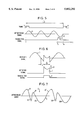
- FIG. 1 is a signal/time diagram related to the method of the present invention in the absence of an interference signal
- FIG. 2 is a signal/time diagram on the occurrence of a once-only-interference signal
- FIG. 4 is a signal/time diagram related to a further embodiment of the method of the present invention on the occurrence of a once-only-interference signal
- FIG. 5 is a signal/time diagram on the occurrence of a sinusoidal interference signal
- FIG. 6 is a portion of a signal/time diagram related to evaluation of the received signals
- FIG. 7 is a typical record of the input signal of the light receiver on receiving light from high frequency lamps.
- FIG. 8 is a block circuit diagram of a light sensor formed in accordance with the present invention.
- the received signal is observed starting with the frame start and is investigated for the reception of interference signals during the frame interval T R in order to determine the ideal timepoint for the transmission of the next light signal independently of an occurring interference signal. If no interference signal occurs up to the end of frame interval T R , then the next light signal is transmitted at its normal transmission timepoint t N as is illustrated in FIG. 1.
- the light signal is illustrated by a rectangular transmitted pulse 2 with the width T S (transmission interval T S ).
- the light signal can however, for example, also be formed by a sequence of light pulses or by a signal of any desired shape.
- a signal value received during the transmission interval T S specifies the presence or the absence of an object in the monitored region depending on whether the method is used with a reflection light sensor or with a transmission light sensor.
- the apparatus After the end of the transmission interval T S , the apparatus is again switched over to receipt and evaluation of an interference signal in order to determine the ideal transmission timepoint for the next transmitted pulse independently of an interference signal arriving in the next frame interval T R . It is however also possible to allow the evaluation of the received signal for the determination of the ideal transmission timepoint to continue to run in parallel during the transmission interval T S so that in this manner, the determination of the ideal transmission timepoint for the next light signal already starts earlier. This is in particular sensible when the transmission of the actual light signal takes place at the end of the frame and the transmission interval T S extends into the start of the next frame.
- a waiting time T C is triggered at the start of the interference signal 3 at the time t 0 . If a signal flank again occurs during the waiting time T C , as is the case at the time t 1 in FIG. 2, then the waiting time is prematurely terminated and started anew.
- the triggering of the waiting time T C can be controlled by the occurrence of signal flanks or also by attaining or exceeding or falling short of preset threshold values.
- a waiting time T C is advantageously only triggered when a positive threshold value is exceeded or a negative threshold value is fallen short of. In this way it is, for example, ensured that transient oscillation processes which die away do not trigger a further waiting time T C .
- the waiting times can, for example, be realized by a counter, as is described in more detail with reference to FIG. 7, with the length of the waiting time T C being definable by a predeterminable count.
- the transmitted transmission pulses of a neighboring light sensor coincide with the respective frame ends, and thus with the transmission timepoints of a light sensor operating in accordance with the method of the present invention in the interference free case, and if these transmitted foreign transmission pulses are received by the light sensor operating in accordance with the present invention as interference signals, then these interference signals cannot be used to determine any ideal transmission timepoints of the light signal.
- the transmitted pulses of the neighboring light sensor received as interference signals can lead to a faulty evaluation of the received light signal since, depending of the nature of the light sensor, the presence or absence of an object in the monitored region can be falsely detected.
- FIG. 4 there is shown a special case of the method described in accordance with FIG. 2 for the treatment in accordance with the invention of once-only-interference signals.
- a waiting time T C is triggered by the end of the interfering pulse 3. Since, in the example in FIG. 4, the end of the waiting time T C would lie timewise after the end of the frame interval T R , the frame interval is in this case extended by the remaining interval T R ' so that the end of the waiting time T c coincides with the end of the total frame interval T R +T R '.
- the transmission pulse 2 is subsequently transmitted, as in the case of FIG. 2.
- the frame interval T R which follows the extended frame interval T R +T R '.again has the original length.
- a periodic sinusoidal signal is illustrated in FIG. 5.
- the received signal is first observed at the start of the frame interval T R and classified in accordance with its nature. This can, for example, take place, as described in connection with FIG. 2, in that waiting times T C are triggered on reading or exceeding or falling short of predetermined threshold values and with the received signal being classified as an alternating interference signal, for example as a sinusoidal interference signal in accordance with FIG. 5 , if more than three waiting times T C are triggered or if a third waiting time T C is prematurely terminated.
- instances of the threshold values being exceeded or fallen short of shortly after each other such as are, for example, present with zero passages of the signal, only trigger one waiting time T C . Fundamentally it is however advantageous when the received signals are cleared of DC components prior to the evaluation.
- the next negative halfwave 5 of the interference signal is found and the next transmitted pulse 2 is transmitted during the duration of the negative halfwave 5.
- the transmission of the transmitted pulse 2 thus takes place at a time t S which is advanced timewise relative to the normal transmission timepoint t N .
- the interference signal contains no negative halfwaves, then the interference signal is exclusively classified by the positive halfwave as an alternating interference signal and, after classification has taken place, the transmitted pulse 2 is transmitted in the next interference-free interval lying being two positive halfwaves.
- the transmission of the transmitted pulse 2 within the negative halfwave, or within the interference-free intermediate interval it is ensured that a faulty recognition of an object present in the monitored region does not take place under any circumstances, as will be explained in more detail herein with reference to FIG. 6.
- FIG. 6 shows, in the upper half, the received signal 6 which is composed of the sinusoidal interference signal 4 of FIG. 5 and the transmitted pulse 2 which is for example, reflected at an object present in the monitored region.
- the transmitted pulse 2 was transmitted during the reception of the negative halfwave of the sinusoidal interference signal 4 at a time interval T D after the start of the negative halfwave so that both the start and also the end of the transmission interval T S come to lie within the reception of the negative halfwave of the sinusoidal interference signal 4.
- the longest negative halfwave is first determined and the transmitted pulses subsequently transmitted during the next longest negative halfwave. If, for example, the second negative halfwave 10' has been recognized as the longer negative halfwave at the time T 2 in FIG. 7, then it is necessary to wait until the next but-one negative halfwave 10'" before transmitting the transmitted pulse 2.
- a count in the rising direction is started by the start of the first positive halfwave 9.
- the counter is reset and a counting procedure is started again which is stopped at the end of the first negative halfwave 10.
- the count which has been reached represents a value representative for the duration of the first negative halfwave 10.
- the counter is, for example, started in the downward direction until the count is stopped again at the start of the next positive halfwave 9". Since the end count is positive at this time, the second negative halfwave 10' is recognized as the longer negative halfwave and the transmitted pulse 2 is transmitted during the next but-one negative halfwave 10'".
- the transmitted pulse 2 is correspondingly transmitted during the next negative halfwave.
- the length of the negative halfwaves can, for example, be detected by storing the counts achieved at the ends of the negative halfwaves and the longest negative halfwave can be determined following recognition of a complete period by comparison of the stored counts.
- the transmitted pulse is then transmitted during the next period of the interference signal during the duration of the longest negative halfwave that has been found.
- the block circuit diagram of a light sensor formed in accordance with the present invention and shown in FIG. 8 includes a light transmitter 11 which transmits a transmitted pulse 2 which is reflected at an object 12 present in the monitored region.
- the reflected transmitted pulse is received together with an interference signal 8 by a light receiver 13, with the output of the light receiver 13 being connected via a line 19 to an interference signal evaluation until 14 and via a first switch 15 to an object signal evaluation unit 16.
- the light transmitter 11 is connected via a second switch 17 to a voltage source U, with the switches 15 and 17 being synchronously actuatable by the interference signal evaluation unit 14.
- the switches 15, 17 are closed so that the light transmitter 11 transmits a transmitted pulse 2 via the voltage U applied to the switch 15, which the transmitted pulse 2 being received by the light receiver 13 and being supplied via a switch 17 to the object signal evaluation unit 16.
- the switches 15, 17 are again opened by the interference signal evaluation unit 14 so that the received interference signals 8 cannot influence the object signal evaluation unit 16.
- the received interference signals 8 are supplied via a line 19 to the signal evaluation unit 14 and are evaluated by the latter for the determination of the ideal transmission timepoint of the next transmitted pulse 2.
- the interference signal evaluation unit 14 includes a counter 18 which is suitable for determining both the length of the negative halfwaves of the interference signals and also for realizing the waiting times T C as has been described with respect to FIGS. 2 to 7.
Landscapes
- Physics & Mathematics (AREA)
- Life Sciences & Earth Sciences (AREA)
- General Life Sciences & Earth Sciences (AREA)
- General Physics & Mathematics (AREA)
- Geophysics (AREA)
- Optical Communication System (AREA)
- Geophysics And Detection Of Objects (AREA)
- Burglar Alarm Systems (AREA)
- Photometry And Measurement Of Optical Pulse Characteristics (AREA)
Applications Claiming Priority (2)
| Application Number | Priority Date | Filing Date | Title |
|---|---|---|---|
| DE19537615.3 | 1995-10-09 | ||
| DE19537615A DE19537615B4 (de) | 1995-10-09 | 1995-10-09 | Verfahren zum Betrieb eines optischen Lichttasters |
Publications (1)
| Publication Number | Publication Date |
|---|---|
| US5852292A true US5852292A (en) | 1998-12-22 |
Family
ID=7774423
Family Applications (1)
| Application Number | Title | Priority Date | Filing Date |
|---|---|---|---|
| US08/727,061 Expired - Lifetime US5852292A (en) | 1995-10-09 | 1996-10-08 | Method of operating an optical light sensor |
Country Status (5)
| Country | Link |
|---|---|
| US (1) | US5852292A (de) |
| EP (1) | EP0768545B1 (de) |
| JP (1) | JPH09133580A (de) |
| DE (2) | DE19537615B4 (de) |
| DK (1) | DK0768545T3 (de) |
Cited By (4)
| Publication number | Priority date | Publication date | Assignee | Title |
|---|---|---|---|---|
| US6411215B1 (en) | 1999-02-19 | 2002-06-25 | J. Mitchell Shnier | Optical methods for detecting the position or state of an object |
| EP1306693A1 (de) * | 2001-10-29 | 2003-05-02 | Sunx Limited | Photoelektrischer Multi-Achsen-Sensor mit Interferenzlichtdetektion |
| US20030128404A1 (en) * | 2002-01-07 | 2003-07-10 | Xerox Corporation | Method and apparatus for eliminating lamp strobing in a digital input scanner |
| CN106289513A (zh) * | 2015-06-29 | 2017-01-04 | 阿自倍尔株式会社 | 光电传感器 |
Families Citing this family (8)
| Publication number | Priority date | Publication date | Assignee | Title |
|---|---|---|---|---|
| DE19926214A1 (de) * | 1999-06-09 | 2001-01-11 | Balluff Gebhard Gmbh & Co | Verfahren zur Unterdrückung von Störsignalen in Optosensoren/Näherungsschaltern und Schaltungsanordnung zur Druchführung dieses Verfahrens |
| DE10011598B4 (de) * | 2000-03-10 | 2010-07-22 | Sick Ag | Optoelektronische Sensoranordnung sowie Verfahren zum Betreiben einer optoelektronischen Sensoranordnung |
| FR2813129B1 (fr) * | 2000-08-16 | 2002-10-11 | Schneider Electric Ind Sa | Disposition anti-interferences pour cellules optiques |
| US20080129500A1 (en) * | 2003-11-10 | 2008-06-05 | Omron Corporation | Processing Device And Object Detection Device |
| DE102006023971B8 (de) * | 2006-05-22 | 2009-04-30 | Pepperl + Fuchs Gmbh | Optischer Sensor und Verfahren zum Nachweis von Personen, Tieren oder Gegenständen |
| DE102008005064B4 (de) | 2008-01-18 | 2010-06-17 | Sick Ag | Optoelektronisches Detektionsverfahren und optoelektronischer Detektor |
| EP3739365B1 (de) * | 2019-05-13 | 2024-04-24 | Leuze electronic GmbH + Co. KG | Optischer sensor |
| DE102019125321A1 (de) * | 2019-09-20 | 2021-03-25 | Sick Ag | Optoelektronische sensoranordnung und sensorsystem |
Citations (6)
| Publication number | Priority date | Publication date | Assignee | Title |
|---|---|---|---|---|
| US4851689A (en) * | 1987-04-15 | 1989-07-25 | Alps Electric Co., Ltd. | Photodetecting circuit |
| US4973834A (en) * | 1987-07-14 | 1990-11-27 | Samsung Electronics Co., Ltd. | Optical switching device employing a frequency synchronous circuit |
| US5099113A (en) * | 1990-05-11 | 1992-03-24 | Idec Izumi Corporation | Photoelectrical switching circuit with frequency divider circuit |
| US5208452A (en) * | 1989-12-20 | 1993-05-04 | Kabushiki Kaisha Topcon | Method and apparatus for reliably detecting light beam in the presence of undesirable light, especially suitable for surveying instruments |
| US5250801A (en) * | 1990-10-02 | 1993-10-05 | Erwin Sick Gmbh Optik Elektronik | Optical sensor for detecting articles in a monitored region and method for operating the same |
| US5550369A (en) * | 1994-02-28 | 1996-08-27 | Electro-Pro, Inc. | Triangulation position detection method and apparatus |
Family Cites Families (6)
| Publication number | Priority date | Publication date | Assignee | Title |
|---|---|---|---|---|
| DE3823007A1 (de) * | 1988-07-07 | 1990-01-11 | Telefunken Electronic Gmbh | Optischer sensor |
| DE4141468C2 (de) * | 1991-12-16 | 1994-06-30 | Sick Optik Elektronik Erwin | Optische Sensoranordnung und Verfahren zu deren Betrieb |
| DE4141469C2 (de) * | 1991-12-16 | 1997-07-17 | Sick Ag | Verfahren zum Betrieb einer optischen Sensoranordnung zur Feststellung von in einem Überwachungsbereich vorhandenen Gegenständen sowie eine solche optische Sensoranordnung |
| DE4237311C1 (de) * | 1992-08-25 | 1993-12-16 | Leuze Electronic Gmbh & Co | Aus einem Sender und einem Empfänger bestehende Einrichtung zum Erfassen von Gegenständen |
| DE4319451C1 (de) * | 1992-11-05 | 1994-08-25 | Leuze Electronic Gmbh & Co | Aus einem Sender und einem Empfänger bestehende Einrichtung zum Erfassen von Gegenständen |
| DE4324590C2 (de) * | 1993-07-22 | 1995-06-08 | Leuze Electronic Gmbh & Co | Lichtschrankenanordnung mit geregelter Ansprechempfindlichkeit |
-
1995
- 1995-10-09 DE DE19537615A patent/DE19537615B4/de not_active Expired - Fee Related
-
1996
- 1996-08-29 DE DE59609323T patent/DE59609323D1/de not_active Expired - Lifetime
- 1996-08-29 EP EP96113873A patent/EP0768545B1/de not_active Expired - Lifetime
- 1996-08-29 DK DK96113873T patent/DK0768545T3/da active
- 1996-10-08 US US08/727,061 patent/US5852292A/en not_active Expired - Lifetime
- 1996-10-09 JP JP26876596A patent/JPH09133580A/ja active Pending
Patent Citations (6)
| Publication number | Priority date | Publication date | Assignee | Title |
|---|---|---|---|---|
| US4851689A (en) * | 1987-04-15 | 1989-07-25 | Alps Electric Co., Ltd. | Photodetecting circuit |
| US4973834A (en) * | 1987-07-14 | 1990-11-27 | Samsung Electronics Co., Ltd. | Optical switching device employing a frequency synchronous circuit |
| US5208452A (en) * | 1989-12-20 | 1993-05-04 | Kabushiki Kaisha Topcon | Method and apparatus for reliably detecting light beam in the presence of undesirable light, especially suitable for surveying instruments |
| US5099113A (en) * | 1990-05-11 | 1992-03-24 | Idec Izumi Corporation | Photoelectrical switching circuit with frequency divider circuit |
| US5250801A (en) * | 1990-10-02 | 1993-10-05 | Erwin Sick Gmbh Optik Elektronik | Optical sensor for detecting articles in a monitored region and method for operating the same |
| US5550369A (en) * | 1994-02-28 | 1996-08-27 | Electro-Pro, Inc. | Triangulation position detection method and apparatus |
Cited By (10)
| Publication number | Priority date | Publication date | Assignee | Title |
|---|---|---|---|---|
| US6411215B1 (en) | 1999-02-19 | 2002-06-25 | J. Mitchell Shnier | Optical methods for detecting the position or state of an object |
| EP1306693A1 (de) * | 2001-10-29 | 2003-05-02 | Sunx Limited | Photoelektrischer Multi-Achsen-Sensor mit Interferenzlichtdetektion |
| US6858832B2 (en) | 2001-10-29 | 2005-02-22 | Sunx Limited | Photoelectric sensor having time changing means |
| EP1548466A1 (de) * | 2001-10-29 | 2005-06-29 | Sunx Limited | Photoelektrischer Multi-Achsen-Sensor mit Interferenzlichtdetektion |
| AU2002301601B2 (en) * | 2001-10-29 | 2007-06-28 | Sunx Limited | Photoelectric Sensor |
| US20030128404A1 (en) * | 2002-01-07 | 2003-07-10 | Xerox Corporation | Method and apparatus for eliminating lamp strobing in a digital input scanner |
| US7042600B2 (en) | 2002-01-07 | 2006-05-09 | Xerox Corporation | Method and apparatus for eliminating lamp strobing in a digital input scanner |
| CN106289513A (zh) * | 2015-06-29 | 2017-01-04 | 阿自倍尔株式会社 | 光电传感器 |
| CN106289513B (zh) * | 2015-06-29 | 2018-08-03 | 阿自倍尔株式会社 | 光电传感器 |
| US10061026B2 (en) | 2015-06-29 | 2018-08-28 | Azbil Corporation | Photoelectric sensor with disturbance detection |
Also Published As
| Publication number | Publication date |
|---|---|
| DE59609323D1 (de) | 2002-07-18 |
| DK0768545T3 (da) | 2002-10-07 |
| EP0768545A2 (de) | 1997-04-16 |
| EP0768545B1 (de) | 2002-06-12 |
| EP0768545A3 (de) | 1999-09-15 |
| JPH09133580A (ja) | 1997-05-20 |
| DE19537615A1 (de) | 1997-04-10 |
| DE19537615B4 (de) | 2005-02-17 |
Similar Documents
| Publication | Publication Date | Title |
|---|---|---|
| US5852292A (en) | Method of operating an optical light sensor | |
| US5250801A (en) | Optical sensor for detecting articles in a monitored region and method for operating the same | |
| KR930005036B1 (ko) | 내연기관의 녹(knock)억제장치 | |
| US20030010891A1 (en) | Photoelectric sensor | |
| EP0802602A3 (de) | Vorrichtung zur Feststellung und zum Ansprechen auf Störlichtbögen in elektrischen Wechselspannungssystemen | |
| CA1268570A (en) | Telephone tone detector | |
| US5243181A (en) | Noise-insensitive, photoelectric transceiver including a digital stability indicator | |
| EP0393558B2 (de) | Vertikalsynchronisierungssignaldetektor | |
| CA1122294A (en) | Power line signalling system | |
| CN1106719C (zh) | 数据传输系统 | |
| NL8401955A (nl) | Schakeling voor het afleiden van een in een inkomend videosignaal aanwezig synchroniseersignaal. | |
| US4729023A (en) | Mode recognition for vertical countdown | |
| US5789740A (en) | Method and device for eliminating interference signals in a light barrier | |
| US6385027B1 (en) | Noise protection device | |
| JPH04271613A (ja) | 光電スイッチ | |
| JPH0870490A (ja) | 赤外線ワイヤレスリモコン信号の受信方法 | |
| SU1075444A1 (ru) | Устройство устранени импульсных помех на изображении | |
| JP2584052B2 (ja) | 通信装置 | |
| SU1019646A1 (ru) | Устройство дл приема и обработки сигналов с импульсной модул цией | |
| JP2762855B2 (ja) | フレーム同期保護回路 | |
| SU1180940A1 (ru) | Устройство дл счета предметов | |
| SU1050123A2 (ru) | Устройство подавлени шумов | |
| JP2003018621A (ja) | プッシュボタン信号受信装置およびプッシュボタン信号検出方法 | |
| SU1601769A1 (ru) | Устройство поиска шумоподобных сигналов | |
| KR0121960B1 (ko) | 링신호 검출 방법 |
Legal Events
| Date | Code | Title | Description |
|---|---|---|---|
| AS | Assignment |
Owner name: SICK AG, GERMANY Free format text: ASSIGNMENT OF ASSIGNORS INTEREST;ASSIGNORS:BLUEMCKE, THOMAS;BURGER, JURGEN;KUHN, FRITZ;AND OTHERS;REEL/FRAME:008232/0839;SIGNING DATES FROM 19960808 TO 19960902 |
|
| STCF | Information on status: patent grant |
Free format text: PATENTED CASE |
|
| FEPP | Fee payment procedure |
Free format text: PAYOR NUMBER ASSIGNED (ORIGINAL EVENT CODE: ASPN); ENTITY STATUS OF PATENT OWNER: LARGE ENTITY |
|
| FPAY | Fee payment |
Year of fee payment: 4 |
|
| SULP | Surcharge for late payment | ||
| FPAY | Fee payment |
Year of fee payment: 8 |
|
| FPAY | Fee payment |
Year of fee payment: 12 |