US5892415A - Laminated resonator and laminated band pass filter using same - Google Patents
Laminated resonator and laminated band pass filter using same Download PDFInfo
- Publication number
- US5892415A US5892415A US08/749,893 US74989396A US5892415A US 5892415 A US5892415 A US 5892415A US 74989396 A US74989396 A US 74989396A US 5892415 A US5892415 A US 5892415A
- Authority
- US
- United States
- Prior art keywords
- electrode
- internal electrodes
- outgoing
- pass filter
- band pass
- Prior art date
- Legal status (The legal status is an assumption and is not a legal conclusion. Google has not performed a legal analysis and makes no representation as to the accuracy of the status listed.)
- Expired - Lifetime
Links
Images


Classifications
-
- H—ELECTRICITY
- H03—ELECTRONIC CIRCUITRY
- H03H—IMPEDANCE NETWORKS, e.g. RESONANT CIRCUITS; RESONATORS
- H03H9/00—Networks comprising electromechanical or electro-acoustic elements; Electromechanical resonators
- H03H9/46—Filters
-
- H—ELECTRICITY
- H03—ELECTRONIC CIRCUITRY
- H03H—IMPEDANCE NETWORKS, e.g. RESONANT CIRCUITS; RESONATORS
- H03H7/00—Multiple-port networks comprising only passive electrical elements as network components
- H03H7/01—Frequency selective two-port networks
- H03H7/0115—Frequency selective two-port networks comprising only inductors and capacitors
-
- H—ELECTRICITY
- H01—ELECTRIC ELEMENTS
- H01P—WAVEGUIDES; RESONATORS, LINES, OR OTHER DEVICES OF THE WAVEGUIDE TYPE
- H01P1/00—Auxiliary devices
- H01P1/20—Frequency-selective devices, e.g. filters
- H01P1/201—Filters for transverse electromagnetic waves
- H01P1/203—Strip line filters
- H01P1/20327—Electromagnetic interstage coupling
- H01P1/20336—Comb or interdigital filters
- H01P1/20345—Multilayer filters
-
- H—ELECTRICITY
- H01—ELECTRIC ELEMENTS
- H01P—WAVEGUIDES; RESONATORS, LINES, OR OTHER DEVICES OF THE WAVEGUIDE TYPE
- H01P7/00—Resonators of the waveguide type
- H01P7/08—Strip line resonators
- H01P7/084—Triplate line resonators
-
- H—ELECTRICITY
- H03—ELECTRONIC CIRCUITRY
- H03H—IMPEDANCE NETWORKS, e.g. RESONANT CIRCUITS; RESONATORS
- H03H1/00—Constructional details of impedance networks whose electrical mode of operation is not specified or applicable to more than one type of network
- H03H2001/0021—Constructional details
- H03H2001/0085—Multilayer, e.g. LTCC, HTCC, green sheets
Definitions
- the present invention relates to a resonator and a band pass filter using the same, and more particularly, to a laminated resonator and a laminated band pass filter using the same, used in a portable telephone set.
- a conventional resonator as shown in FIG. 16 includes a dielectric substrate 192 having a conductor 93 over the entire back thereof and a strip conductor 94 on the surface thereof.
- the resonator further comprises another dielectric substrate 192 having a conductor 93 over the entire surface thereof, bonded to the first-mentioned substrate 192 with the strip conductor 94 in between to achieve a laminated structure.
- the length of this strip conductor 94 is L
- the central wavelength of the resonator is ⁇
- the specific inductive capacitance of the dielectric substrate is ⁇
- the strip conductor 94 is required to have a length L satisfying the relationship of the formula (1). Further, the strip conductor 94 and other resonator parts are typically configured to satisfy strict dimensional tolerances, thereby rendering the manufacture of the resonator difficult.
- Another conventional band pass filter as shown in FIG. 38, comprises a dielectric substrate 102 having conductor 103 over the entire back thereof, and two strip conductors 104 which are ⁇ /4 resonators on the surface of the dielectric substrate.
- the two strip conductors 104 are configured to be separated by a distance (D) of about ⁇ /4.
- the band pass filter further comprises another dielectric substrate 102 having a conductor 103 over the entire surface thereof, bonded to the first dielectric substrate 102 with the strip conductors 104 in between to achieve a laminated structure. Assuming that the length of the strip conductors 104 is L, the central wavelength is ⁇ , and the specific inductive capacity of the dielectric substrate is ⁇ , then the foregoing formula (1) applies.
- An object of the present invention is therefore to provide a laminated resonator and a laminated band pass filter using such a laminated resonator, which can be easily downsized and which is easy to manufacture.
- exemplary embodiments of a laminated resonator according to the present invention comprise:
- a laminated resonator in which the third external electrode is used as an input/output external electrode, and at least one of the first external electrode and the second external electrode is used as a grounding external electrode.
- Another exemplary embodiment of the laminated resonator includes electric coupling between said at least one internal electrode and an outgoing electrode, which is at least one of capacitive coupling, inductive coupling and direct coupling.
- the outgoing electrode can be arranged between the internal electrodes, or outside the internal electrodes.
- a laminated resonator in which a shielded electrode is provided on at least one of an upper and a lower surface of the lamination.
- This shielded electrode can be connected to at least one of the first and the second external electrodes, or connected to none of these electrodes.
- the distance between the shielded electrode and a proximate internal electrode can, for example, be at least 300 ⁇ m, or greater.
- Exemplary embodiments of the present invention further encompass the use of a laminated band pass filter having at least two resonators, in which each of the resonators has at least a pair of oppositely arranged internal electrodes and an outgoing electrode electrically coupled with at least one of the internal electrodes.
- the band pass filter further includes a first external electrode connected to at least one of the internal electrodes of each resonator, a second external electrode connected to another of the internal electrodes of each resonator, and third and a fourth external electrodes connected to the respective outgoing electrodes of the resonators.
- the external electrodes are provided, at least in part, on a surface of a lamination formed by the internal electrodes, the outgoing electrodes and an insulator.
- the third and fourth external electrodes are used as input/output external electrodes, and at least one of the first and the second external electrodes is used as a grounding external electrode.
- Another exemplary embodiment of the laminated band pass filter includes, for each of the plural resonators, electric coupling between the internal electrode and the outgoing electrode which is at least one of capacitive coupling, inductive coupling and direct coupling.
- the outgoing electrode can be provided between the internal electrodes or outside the internal electrodes.
- a laminated band pass filter in which a shielded electrode is provided on at least one of an upper and a lower surfaces of the lamination.
- This shielded electrode can be connected to at least one of the first and the second external electrodes, or connected to none of these electrodes.
- the distance between the shielded electrode and a proximate internal electrode can, for example, be at least 300 ⁇ m, or greater.
- Exemplary embodiments of present invention further encompass the use of a laminated band pass filter in which the first and the second external electrodes are formed on opposite side surfaces of the lamination, and the internal electrodes extend to the respective opposite surfaces, and are connected to the first and the second external electrodes, respectively.
- Exemplary embodiments as described above form a distribution constant resonator using capacitance generated between the internal electrodes, combined with inductance possessed by the internal electrodes.
- a plurality of distribution constant resonators can be converted into a multiple-stage band pass filter by inductive coupling and capacitive coupling.
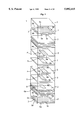
- FIG. 1 is an exploded perspective view illustrating a first embodiment of the laminated resonator of the present invention
- FIG. 2 is a perspective view illustrating the laminated resonator shown in FIG. 1;
- FIG. 3 is a sectional view of the laminated resonator shown in FIG. 2 cut along the line III--III;
- FIG. 4 is an exploded perspective view illustrating a second embodiment of the laminated resonator of the present invention.
- FIG. 5 is a sectional view of the laminated resonator shown in FIG. 4;
- FIG. 6 is an exploded perspective view illustrating a third embodiment of the laminated resonator of the present invention.
- FIG. 7 is a sectional view of the laminated resonator shown in FIG. 6;
- FIG. 8 is an exploded perspective view illustrating a fourth embodiment of the laminated resonator of the present invention.
- FIG. 9 is a sectional view of the laminated resonator shown in FIG. 8.
- FIG. 10 is an exploded perspective view illustrating a fifth embodiment of the laminated resonator of the present invention.
- FIG. 11 is a sectional view of the laminated resonator shown in FIG. 10;
- FIG. 12 is an exploded perspective view illustrating a sixth embodiment of the laminated resonator of the present invention.
- FIG. 13 is a sectional view of the laminated resonator shown in FIG. 12;
- FIG. 14 is an exploded perspective view illustrating a seventh embodiment of the laminated resonator of the present invention.
- FIG. 15 is a sectional view of the laminated resonator shown in FIG. 14;
- FIG. 16 is an exploded perspective view illustrating a conventional laminated resonator
- FIG. 17 is an exploded perspective view illustrating a first embodiment of the laminated band pass filter of the present invention.
- FIG. 18 is a perspective view illustrating the laminated band pass filter shown in FIG. 17;
- FIG. 19 is a sectional view of the band pass filter shown in FIG. 18 cut along the line III--III;
- FIG. 20 is a graph illustrating damping and loss characteristics of the filter shown in FIG. 18;
- FIG. 21 is an exploded perspective view illustrating a second embodiment of the laminated band pass filter of the present invention.
- FIG. 22 is a sectional view of the laminated band pass filter shown in FIG. 21;
- FIG. 23 is an exploded view illustrating a third embodiment of the laminated band pass filter of the present invention.
- FIG. 24 is a sectional view of the laminated band pass filter shown in FIG. 23;
- FIG. 25 is an exploded perspective view illustrating a fourth embodiment of the laminated band pass filter of the present invention.
- FIG. 26 is a graph illustrating damping and loss characteristics of the filter shown in FIG. 25;
- FIG. 27 is an exploded perspective view illustrating a fifth embodiment of the laminated band pass filter of the present invention.
- FIG. 28 is an exploded perspective view illustrating a sixth embodiment of the laminated band pass filter of the present invention.
- FIG. 29 is an exploded perspective view illustrating a seventh embodiment of the laminated band pass filter of the present invention.
- FIG. 30 is a graph illustrating damping and loss characteristics of the filter shown in FIG. 29;
- FIG. 31 is an exploded perspective view illustrating an eighth embodiment of the laminated band pass filter of the present invention.
- FIG. 32 is a graph illustrating damping and loss characteristics of the filter shown in FIG. 31;
- FIG. 33 is an exploded perspective view illustrating a ninth embodiment of the laminated band pass filter of the present invention.
- FIG. 34 is an exploded perspective view illustrating a tenth embodiment of the laminated band pass filter of the present invention.
- FIG. 35 is an exploded perspective view illustrating an eleventh embodiment of the laminated band pass filter of the present invention.
- FIG. 36 is an exploded perspective view illustrating a twelfth embodiment of the laminated band pass filter of the present invention.
- FIG. 37 is an exploded perspective view illustrating a thirteenth embodiment of the laminated band pass filter of the present invention.
- FIG. 38 is an exploded perspective view illustrating a conventional laminated band pass filter.
- a laminated resonator 1 comprises a dielectric sheet 2 having internal electrodes 4 and 5 on the surface thereof, a dielectric sheet 2 having an outgoing electrode 6 on the surface thereof, a dielectric sheet 2 having a shielded electrode 3 on the surface thereof, and a dielectric sheet 2 having nothing formed on the surface thereof.
- the dielectric sheet 2 is formed by kneading a mixture of a ceramic powder and a bonding agent, and forming the kneaded mixture into the shape of a sheet.
- the electrodes 3 to 6 can, for example, comprise Ag, Cu, Au or Ag--Pd, and are formed by such techniques as printing, sputtering or vapor deposition.
- the internal electrode 4 is rectangular, and has an end portion 4a exposed on one side of the sheet 2, and the other end portion 4b forming an open end.
- the internal electrode 5 forms a pair with the internal electrode 4 and is arranged opposite to the internal electrode 4.
- the internal electrode 5 also has an end portion 5a exposed on one side of the sheet 2, and has another end portion 5b forming an open end.
- the internal electrode 4 is designed to have a width slightly larger than the width of the internal electrode 5. This is to ensure stable manufacture of a resonator of a constant resonance frequency, even upon the occurrence of a shift in laminating the sheet 2, by preventing the facing area between the internal electrodes 4 and 5 from varying.
- the shape of the internal electrodes 4 and 5 is not limited to a rectangle, but may be circular, triangular, polygonal, or other shape.
- the outgoing electrode 6 has an end portion 6a exposed on the left side of the sheet 2, and the other end portion 6b has a large width to provide an increased area.
- the end portion 6b is coupled with the internal electrode 5 by capacity coupling. It is not, however, necessary to provide an increased area at the end portion 6b of the outgoing electrode 6.
- the outgoing electrode may be strip-shaped with a constant width. Furthermore, it is not necessary to position the outgoing electrode close to the internal electrode 5. For instance, the outgoing electrode may be positioned in the vicinity of the internal electrode 4, or between the internal electrodes 4 and 5.
- the shielded electrode 3 is formed over substantially the entire surface of the sheet 2, and has an end portion 3a exposed on one side of the sheet 2, and has another end portion 3b exposed on the opposite side.
- the bonding strength between layers is improved by providing portions 3c and 3d, which lack the shielded electrode 3 formed on the outer periphery of the sheet 2.
- the shielded electrode 3 and the sheet 2 are made of different materials, resulting in a low bonding strength. Hence, forming the shielded electrode 3 over the entire surface of the sheet 2 may easily cause peeling or like problems. If there is no risk of peeling, however, the shielding electrode can be formed over the entire surface of the sheet 2.
- the sheets 2 which have the construction as described above, are integrally sintered, after piling, into a lamination. Then, grounding external electrodes 7 and 8 (as shown in FIG. 2) are formed on opposite sides of the resultant lamination, and an input/output electrode 9 is formed on the left side (that is, the left side of the graphical depiction shown in FIG. 2).
- the external electrodes 7 to 9 are formed by such exemplary techniques as coating/baking, sputtering or vapor deposition.
- the end 4a of the internal electrode 4 and the end 3a of the shielded electrode 3 are connected to the grounding external electrode 7, and the end 5a of the internal electrode 5 and the end 3b of the shielded electrode 3 are connected to the grounding external electrode 8.
- the distance d between the shielded electrode 3 and the internal electrodes 4 and 5 can be at least 300 ⁇ m or more.
- the distance d can be at least 400 ⁇ m, or at least 600 ⁇ m, or even at least 800 ⁇ m.
- a small distance d causes the generation of an eddy current loss in the shielded electrode 3, leading to attenuation of a magnetic field in the resonator, which results in deterioration of the Q-value of the resonator.
- a distribution constant resonator 1 In a laminated resonator 1 described above, capacitance produced between the internal electrodes 4 and 5 and inductance possessed by the internal electrodes 4 and 5 are combined to form a distribution constant resonator. More specifically, since this is a distribution constant type resonator with capacitance as a main factor, without the use of a strip conductor as in a conventional resonator, the central wavelength ⁇ is no longer critical, and it is thus possible to downsize the resonator 1. A compact resonator having a high Q-value is thus attainable. Numerically, as compared with a Q-value of 80 for the conventional resonator, the resonator 1 of the first embodiment has an exemplary Q-value of 100.
- a laminated resonator 21 has the same construction as the resonator of the foregoing first embodiment, except for an outgoing electrode 22.
- the outgoing electrode 22 is substantially T-shaped, and has an end portion 22a exposed on the left side of a dielectric sheet 2 and another end portion 22b exposed on another side of the sheet 2.
- the other end portion 22b in the laminated state is coupled with an internal electrode 5 by inductive coupling.
- the end portion 22a is connected to an input/output external electrode 9, and the end portion 22b is connected to a grounding external electrode 8.
- the outgoing electrode may be L-shaped. It is also not necessary that the outgoing electrode be arranged proximate to the internal electrode 5. For instance, it may be arranged in the vicinity of the internal electrode 4 or between the internal electrodes 4 and 5.
- the laminated resonator 21 having the construction as described above functions in a similar manner to the resonator 1 of the above-mentioned first embodiment.
- a laminated resonator 31 has the same construction as that of the resonator 1 of the foregoing first embodiment, except for an outgoing electrode 32.
- the outgoing electrode 32 is formed on a dielectric sheet 2 on which an internal electrode 5 is formed.
- the outgoing electrode 32 is strip-shaped with a constant width, and has an end portion 32a exposed on the left side of the dielectric sheet 2, and has another end portion 32b connected to the internal electrode 5 so as to form substantially a T shape. Therefore, the outgoing electrode 32 is coupled directly with the internal electrode 5.
- the end portion 32a is connected to an input/output external electrode 9. It is not necessary, however, to connect the outgoing electrode to the internal electrode 5. For instance, it can be connected to an internal electrode 4.
- the laminated resonator 31 having the construction as described above has similar functions as the resonator 1 of the above-mentioned first embodiment.
- a laminated resonator 41 has the same construction as that of the resonator 1 of the foregoing first embodiment, but excludes the shielded electrode 3 arranged on the upper surface of the resonator 1.
- a laminated resonator 51 has the same construction as that of the resonator 1 of the first embodiment, but excludes all the shielded electrodes 3 of the resonator 1.
- These resonators 41 and 51 have similar functions as the resonator 1 of the foregoing first embodiment.
- the resonator can be shielded by covering the resonator with a shielding metal case after mounting it on a printed circuit board, or by mounting the resonator 41 or 51 by soldering it onto a wide-area shielding ground pattern formed on a printed circuit board.
- a laminated resonator 61 has the same construction as the resonator 1 of the foregoing first embodiment, except for a shielded electrode 62.
- the shielded electrode 62 is formed over substantially the entire surface of a dielectric sheet 2, and has an end portion 62a which is exposed on one side of the sheet 2. Bonding strength between layers is improved by providing portions 62b and 62c which do not have the shielded electrode 62 formed thereon on the outer periphery of the sheet 2.
- the shielded electrode 62 is connected only to the grounding external electrode 7.
- a laminated resonator 71 has the same construction as the resonator 1 of the foregoing first embodiment, except for a shielded electrode 72.
- the shielded electrode 72 is formed over substantially the entire surface of a dielectric sheet 2. Bonding strength between sheets 2 is improved by providing a portion 72a which does not have the shielded electrode 72 formed thereon on the outer periphery of the sheet 2.
- the shielded electrode 72 is not connected to any external electrode.
- the resonators 61 and 71, having the construction as described above, have similar functions as the resonator 1 of the above-mentioned first embodiment, and further provide an improved bonding strength between sheets 2.
- the laminated resonator of the present invention is not limited to the foregoing embodiments. Many variations are possible, as will be apparent to those skilled in the art.
- the number of internal electrodes is not limited to 4, but can be any number of at least 2 electrodes.
- the central frequency of the resonator can be reduced, and any resonator in a range from MHz to GHz bands can be freely designed without scaling up the size by adjusting the number of internal electrodes.
- the resonator of the present invention is therefore widely applicable, not only in communication equipment, but also in television equipment. Distance between internal electrodes can be non-uniform, and can vary in response to particular specifications.
- external electrodes may be formed on the surface and the back of the lamination by through use of electric connection means, such as through-holes.
- a laminated resonator may be manufactured by the following method.
- the method comprises applying a dielectric pasty material by printing or like technique, forming a dielectric film by drying, applying a conductive pasty material onto the surface of the resultant dielectric film, and drying the film, thereby forming an electrode film.
- a resonator having a lamination structure can thus be obtained by conducting lap coating. It is not necessary to use a dielectric material or ceramics for the sheet 2. For instance, a resin film or any other insulator can be used, or a previously sintered ceramic material can be used.
- Electric coupling between the internal electrode and the outgoing electrode can be any combination of, for example, capacitance coupling and inductive coupling, or any combination of capacitance coupling, inductive coupling and direct coupling.
- a laminated band pass filter 101 comprises a dielectric sheet 2 having internal electrodes 4 (4 1 , 4 2 ) and 5 (5 1 , 5 2 ) on the surface thereof, a dielectric sheet 2 having outgoing electrodes 6 (6 1 , 6 2 ) on the surface thereof, a dielectric sheet 2 having a shielded electrode 3 on the surface thereof, and a dielectric sheet 2 having nothing formed on the surface thereof.
- the dielectric sheet 2 is formed by kneading a mixture of a ceramic powder and a bonding agent and forming the kneaded mixture into the shape of a sheet.
- the electrodes 3 to 6 can comprise, for example, Ag, Cu, Au or Ag--Pd, and are formed by techniques such as printing, sputtering or vapor deposition.
- the internal electrode 4 is rectangular, and has an end portion 4a exposed on one side of the sheet 2, and has another end portion 4b forming an open end.
- the internal electrodes 4 1 and 4 2 are designed with similar dimensions and are installed in parallel with each other.
- the internal electrode 4 1 is positioned toward the left of the sheet 2, and the internal electrode 4 2 is positioned toward the right.
- the internal electrode 5 forming a pair with the internal electrode 4 is rectangular, and is arranged opposite to the internal electrode 4.
- the internal electrode 5 has an end portion 5a exposed on one side of the sheet 2, and has another end portion 5b forming an open end.
- the internal electrodes 5 1 and 5 2 are designed with similar dimensions and are installed in parallel with each other.
- the internal electrode 5 1 is positioned toward the left of the sheet 2, and the internal electrode 5 2 is positioned toward the right.
- the internal electrode 4 is designed to have a width slightly larger than the width of the internal electrode 5. This is to ensure stable manufacture of a band pass filter of a constant resonance frequency, even upon the occurrence of a shift in laminating the sheet 2, by preventing the facing area between the internal electrodes 4 and 5 from varying.
- the shape of the internal electrodes 4 and 5 is not limited to a rectangle. For instance, the shape may be circular, triangular, polygonal, or other shape.
- the outgoing electrode 6 1 has an end portion 6a exposed on the left side of the sheet 2, and has another end portion 6b having a large width to provide an increased area.
- the other end portion 6b is coupled with the internal electrode 5 1 by capacitance coupling.
- the outgoing electrode 6 2 is designed having similar dimensions to the outgoing electrode 6 1 .
- the electrode 6 2 has an end portion 6a exposed on the right side of the sheet 2, and has another end portion 6b coupled with the internal electrode 5 2 by capacitance coupling. It is not, however, necessary to provide an increased area at the end portion 6b.
- the outgoing electrode can be strip-shaped with a constant width. Furthermore, it is not necessary to position the outgoing electrode close to the internal electrode 5.
- the outgoing electrode can be arranged in the vicinity of the internal electrode 4, or between the internal electrodes 4 and 5.
- the shielded electrode 3 is formed over substantially the entire surface of the sheet 2, and has an end portion 3a exposed on one side of the sheet 2, and another end portion 3b exposed on the opposite side.
- the bonding strength between layers is improved by providing portions 3c and 3d which do not have the shielded electrode 3 formed thereon on the outer periphery of the sheet 2.
- the shielded electrode 3 and the sheet 2 are made of different materials, resulting in a low bonding strength. Hence, forming the shielded electrode 3 over the entire surface of the sheet 2 may cause peeling or similar problems. However, if there is no risk of peeling, the shielded electrode 3 may be formed over the entire surface of the sheet 2.
- the sheets 2 having the construction as described above are integrally sintered, after piling, into a lamination. Then, as shown in FIG. 18, grounding external electrodes 7 and 8 are formed on opposite sides of the resultant lamination, respectively, and input/output electrode 9 and 10 are formed on the left and the right sides, respectively.
- the external electrodes 7 to 10 are formed by such exemplary techniques as coating/baking, sputtering or vapor deposition.
- the end 4a of the internal electrode 4 and the end 3a of the shielded electrode 3 are connected to the grounding external electrode 7, and the end 5a of the internal electrode 5 and the end 3b of the shielded electrode 3 are connected to the grounding external electrode 8.
- the end 6a of the outgoing electrode 6 1 is connected to the input/output external electrode 9.
- the distance d between the shielded electrode 3 and the internal electrodes 4 and 5 can be at least 300 ⁇ m, or more. In other embodiments, the distance d can be at least 400 ⁇ m, or at least 600 ⁇ m, or even at least 800 ⁇ m or more.
- a small distance d causes generation of an eddy current loss in the shielded electrode 3, leading to attenuation of a magnetic field in the resonator, results in deterioration of the Q-value of the resonator.
- a laminated band pass filter 101 thus obtained, capacitance produced between the internal electrodes 4 1 and 5 1 and inductance possessed by the internal electrodes 4 1 and 5 1 are combined to form a distribution constant resonator. Similarly, capacitance produced between the internal electrodes 4 2 and 5 2 and inductance possessed by the internal electrodes 4 2 and 5 2 are combined to form a distribution constant resonator. The thus formed two distribution constant resonators are coupled by inductance coupling and capacitance coupling to form a filter known as a two-stage band pass filter.
- this is a distribution constant band pass filter with capacitance as a main factor, without the use of a strip conductor as in a conventional device, the central wavelength ⁇ is no longer critical, and it is thus possible to downsize the band pass filter 101. A compact band pass filter having slight loss is thus possible. Furthermore, because the dimensional tolerances are less strict for the internal electrodes 4 and 5, and the method of manufacturing a conventional laminated condenser is applicable, it is easier to manufacture the laminated band pass filter.
- FIG. 20 is a graph illustrating damping characteristics (solid line 15) and reflection characteristics (solid line 16) of the resultant band pass filter.
- the damping characteristics represented by the broken line 17 are that of a filter obtained in a fifth embodiment described later.
- a laminated band pass filter 121 has the same construction as the band pass filter 101 of the foregoing first embodiment, except for an outgoing electrode 22 (22 1 , 22 2 ).
- the outgoing electrode 22 1 is substantially T-shaped, and has an end portion 22a exposed on the left side of a dielectric sheet 2 and has another end portion 22b exposed on another side of the sheet 2.
- the other end portion 22b is coupled with an internal electrode 5 1 by inductive coupling.
- the outgoing electrode 22 2 is designed having similar dimensions to the outgoing electrode 22 1 , having an end portion 22a exposed on the right side of the sheet 2, and another end portion 22b exposed on another side of the sheet 2.
- the other end portion 22b is coupled with the internal electrode 5 2 by inductive coupling.
- the end portion 22a of the outgoing electrode 22 1 is connected to an input/output external electrode 9, and the end portion 22b is connected to a grounding external electrode 8.
- the end portion 22a of the outgoing electrode 22 2 is connected to the input/output electrode 10, and the end portion 22b is connected to the grounding external electrode 8.
- the outgoing electrode can be L-shaped.
- the outgoing electrode be positioned close to the internal electrode 5.
- the outgoing electrode can be arranged in the vicinity of the internal electrode 4 or between the internal electrodes 4 and 5.
- the laminated band pass filter 121 having the construction as described above has similar functions as the band pass filter 101 of the above-mentioned first embodiment.
- a laminated band pass filter 131 has the same construction as that of the band pass filter 101 of the foregoing first embodiment, except for an outgoing electrode 32 (32 1 , 32 2 ).
- the outgoing electrode 32 is formed on a dielectric sheet 2 on which an internal electrode 5 is formed.
- the outgoing electrode 32 1 is strip-shaped with a constant width, and has an end portion 32a exposed on the left side of the dielectric sheet 2, and has another end portion 32b connected to the internal electrode 5 1 so as to form substantially a T shape. Therefore, the outgoing electrode 32 1 is coupled directly to the internal electrode 5 1 .
- the end portion 32a is connected to an input/output external electrode 9.
- the outgoing electrode 32 2 is designed to have similar dimensions to the outgoing electrode 32 1 , and has an end portion 32a exposed on the right side of the sheet 2, and has another end portion 32b connected to the internal electrode 5 2 . Therefore, the outgoing electrode 32 2 is connected directly to the internal electrode 5 2 .
- the end portion 32a is connected to the input/output external electrode 10. It is not, however, necessary to connect the outgoing electrode to the internal electrode 5. Instead, it may be connected to the internal electrode 4.
- the laminated band pass filter 131 having the construction as described above has similar functions as the band pass filter 101 of the above-mentioned first embodiment.
- a laminated band pass filter 141 has the same construction as that of the band pass filter 101 of the foregoing first embodiment, except for internal electrodes 4 2 and 5 2 .
- the internal electrode 4 2 has an end portion 4a exposed on one side of the sheet 2.
- the internal electrodes 4 1 and 4 2 are formed on the same sheet surface 2, but the electrodes extend to opposite sides thereof.
- the internal electrodes 5 1 and 5 2 are formed on another sheet surface 2 in a similar manner. However, the pairs of electrodes (4 1 and 5 1 ) and (4 2 and 5 2 ) extend to opposite sides of their respective surfaces 2.
- the internal electrode 5 1 capacitance-coupled to an outgoing electrode 6 1 extends to and is exposed on one side of the lamination.
- the internal electrode 5 2 capacitance-coupled to an outgoing electrode 6 2 extends to and is exposed on the opposite side of the lamination.
- the end portion 4a of the internal electrode 4 2 is connected to a grounding external electrode 8 formed on one side of the lamination, and the end portion 5a of the internal electrode 5 2 is connected to a grounding external electrode 7 formed on the opposite side of the lamination.
- FIG. 26 is a graph illustrating damping characteristics (solid line 44) and reflection characteristics (solid line 45) of the thus obtained band pass filter 141.
- the damping characteristics are such that a pole is produced (at the position shown by A in FIG. 26) on the higher-frequency side relative to the central frequency of the filter 141.
- the band pass filter 141 therefore has similar functions to those of the band pass filter 101 of the foregoing first embodiment, with improved damping characteristics.
- a laminated band pass filter 151 comprises three resonators formed by arranging internal electrodes 4 (4 1 , 4 2 , 4 3 ) and 5 (5 1 , 5 2 , 5 3 ) in parallel with respective dielectric sheets 2.
- the internal electrode 4 has an end portion 4a exposed on the one side of the sheet 2.
- the internal electrode 5 opposite to this internal electrode 4 has an end portion 5a exposed on the opposite side of the sheet 2.
- the internal electrodes 4 1 and 5 1 are arranged at positions toward the left of the sheet 2, the internal electrodes 4 2 and 5 2 at the center of the sheet 2, and the internal electrodes 4 3 and 5 3 , toward the right of the sheet 2.
- Outgoing electrodes 6 1 and 6 2 are capacitance-coupled to the internal electrodes 5 1 and 5 3 , respectively.
- the sheets 2 are integrally sintered into a lamination.
- grounding external electrodes 7 and 8 are formed on opposite sides of the lamination, and input/output external electrodes 9 and 10 are formed on the left and the right sides thereof (see FIG. 18).
- the end portion 4a of the internal electrode 4 and the end portion 3a of the shielded electrode 3 are connected to the grounding external electrode 7, and the end portion 5a of the internal electrode 5 and the end portion 3b of the shielded electrode 3 are connected to the grounding electrode 8.
- the end portion 6a of the outgoing electrode 6 1 is connected to the input/output external electrode 9, and the end portion 6a of the outgoing electrode 6 2 is connected to the input/output external electrode 10.
- the resultant band pass filter 151 capacitance produced between the internal electrodes 4 1 and 5 1 and inductance possessed by the internal electrode 4 1 and 5 1 are combined, thereby forming a distribution constant resonator.
- the internal electrodes 4 2 and 5 2 and the internal electrodes 4 3 and 5 3 form distribution constant resonators, respectively.
- the thus formed three resonators are coupled by inductive coupling and capacitance coupling to form a filter known as a three-stage band pass filter.
- the damping characteristics of this band pass filter 151 are represented by the broken line 17 in FIG. 20.
- This band pass filter 151 which does not use a conventional strip conductor, can be manufactured as a compact product with a low resistance component. This embodiment therefore provides a compact three-stage band pass filter with a low loss by arranging the internal electrodes 4 and 5 in parallel.
- a laminated band pass filter 56 has the same construction as that of the band pass filter 151 of the foregoing fifth embodiment, except for internal electrodes 4 2 and 5 2 .
- the internal electrode 4 2 has an end portion 4a exposed on one side of a sheet 2.
- the internal electrodes 4 1 and 4 3 are formed on the same sheet 2 surface as electrode 4 2 , but extend to the opposite side of the sheet 2.
- the end portion 5a of the internal electrode 5 2 is partially exposed on the same side of the sheet 2 as electrodes 4 1 and 4 3 .
- the internal electrodes 5 1 and 5 3 extend to the opposite side of the sheet 2.
- the internal electrodes 5 1 and 5 3 are capacitive-coupled to outgoing electrodes 6 1 and 6 2 and extend to one side of the lamination.
- An end portion 4a of the internal electrode 4 2 is connected to a grounding external electrode 8 formed on one side of the lamination, and an end portion 5a of the internal electrode 5 2 is connected to a grounding external electrode 7 formed on the opposite side of the lamination.
- the thus obtained band pass filter 56 has damping characteristic as represented by the broken line 17 in FIG. 20 such that a pole is formed on the higher-frequency side relative to the central frequency of the filter 56.
- the band pass filter 56 has therefore similar functions to the band pass filter 151 of the foregoing fifth embodiment.
- a laminated band pass filter 161 has the same construction as that of the band pass filter 151 of the foregoing fifth embodiment, except for internal electrodes 4 3 and 5 3 .
- the internal electrode 4 3 has an end portion 4a exposed on one side of the sheet 2.
- the internal electrodes 4 1 and 4 2 formed on the same sheet 2 surface extend to the opposite side of the sheet 2.
- the internal electrode 5 3 has an end portion 5a exposed on the same side of the sheet 2 as electrodes 4 1 and 4 2 .
- the internal electrodes 5 1 and 5 2 formed on the same sheet 2 surface extend to the opposite side of the sheet 2 as electrode 5 3 .
- the internal electrode 5 1 (the internal electrode 5 1 arranged in the lower portion in FIG. 29) is capacitive-coupled with an outgoing electrode 6 1 and extends to and is exposed on one side of the lamination.
- the internal electrode 5 3 (the internal electrode 5 3 arranged in the lower portion in FIG. 29) is capacitive-coupled with an outgoing electrode 6 2 and extends to and is exposed on the opposite side of the lamination.
- the end portion 4a of the internal electrode 4 3 is connected to a grounding external electrode 8 formed on one side of the lamination, and the end portion 5a of the internal electrode 5 3 is connected to a grounding external electrode 7 formed on the opposite side of the lamination.
- FIG. 30 is a graph illustrating damping characteristics (solid line 64) and reflection characteristics (solid line 65) of the resultant band pass filter 161.
- a pole is produced on the lower-frequency side relative to the central frequency of the filter 161 (at the position shown by B in FIG. 30).
- a laminated band pass filter 66 comprises four resonators formed by arranging internal electrodes 4 (4 1 , 4 2 , 4 3 , 4 4 ) and 5 (5 1 , 5 2 , 5 3 , 5 4 ) in parallel on the surface of dielectric sheets 2, respectively.
- the internal electrode 4 has an end portion 4a exposed on one side of the sheet 2, and the internal electrode 5 opposed to this internal electrode 4 has an end portion 5a exposed on the opposite side of the sheet 2.
- Outgoing electrodes 6 1 and 6 2 are capacitance-coupled with the internal electrodes 5 1 and 5 4 , respectively.
- grounding external electrodes 7 and 8 are formed on opposite sides of the lamination, respectively, and input/output external electrodes 9 and 10 are formed on the left and the right sides, respectively (see FIG. 18).
- the end portion 4a of the internal electrode 4 and the end portion 3a of the shielded electrode 3 are connected to the grounding external electrode 7, and the end portion 5a of the internal electrodes 5 and the end portion 3b of the shielded electrode 3 are connected to the grounding external electrode 8.
- the end portion 6a of the outgoing electrode 6 1 is connected to the input/output electrode 9, and the end portion 6a of the outgoing electrode 6 2 is connected to the input/output external electrode 10.
- FIG. 32 is a graph illustrating damping characteristics (solid line 69) and reflection characteristics (solid line 70) of the band pass filter 66.
- the damping characteristics are such that a pole is produced on the high-frequency side and the low-frequency side (at the positions represented by C and D, respectively, in FIG. 32) with the central frequency of the filter 66 in between, with an excellent damping characteristic.
- the band pass filter 66 which does not use a conventional strip conductor, can be manufactured into a compact product having a slight resistance component. It is therefore possible to easily obtain a compact four-stage band pass filter by arranging the internal electrodes 4 and 5 in parallel with a low loss.
- a laminated band pass filter 171 has the same construction as that of the band pass filter 66 of the foregoing eighth embodiment, except for internal electrodes 4 2 , 4 4 , 5 2 and 5 4 .
- Each of the internal electrodes 4 2 and 4 4 have an end portion 4a exposed on one side of a sheet 2.
- the internal electrodes 4 1 and 4 3 are formed on the same sheet 2 surface, but extend to the opposite side of the sheet 2.
- Each of the internal electrodes 5 2 and 5 4 has an end portion 5a exposed on one side of the sheet 2.
- the internal electrodes 5 1 and 5 3 are formed on the same sheet 2, but extend to the opposite side of the sheet 2.
- the internal electrode 5 1 (the internal electrode 5 1 arranged in the lower portion in FIG. 33) is capacitive-coupled with an outgoing electrode 6 1 , and extends to and is exposed on one side of the lamination.
- the internal electrode 5 4 (the internal electrode 5 4 arranged in the lower portion in FIG. 33) is capacitive-coupled with an outgoing electrode 6 2 , and extends to and is exposed on the opposite side of the lamination.
- the end portions 4a of the internal electrodes 4 2 and 4 4 are connected to a grounding electrode 8 formed on one side of the lamination, and the end portions 5a of the internal electrodes 5 2 and 5 4 are connected to a grounding electrode 7 formed on the opposite side of the lamination.
- the resultant band pass filter 171 has damping and reflection characteristics similar to those shown in the graph of FIG. 32.
- the band pass filter 171 has similar functions to the band pass filter 66 of the foregoing eighth embodiment.
- the internal electrodes formed on the sheets 2 extend alternately to opposite sides.
- This embodiment is not, however, limited to this specific configuration. For instance, every two internal electrodes may alternately extend; for example, 4 1 and 4 2 may extend to one side of the sheet 2, and 4 3 and 4 4 may extend to the opposite side.
- a laminated band pass filter 76 has the same construction as that of the band pass filter 101 of the foregoing first embodiment, but excludes the shielded electrode 3 arranged on the upper surface of the filter 101.
- a laminated band pass filter 81 has the same construction as the band pass filter 101 of the foregoing first embodiment, but excludes all the shielded electrodes 3 of the filter 101.
- the band pass filter 76 or 81 can be shielded by covering it with a shielding metal case after mounting it onto a printed circuit board, or by mounting the filter 76 or 81 by soldering it onto a ground pattern for shielding having a wide area formed on a printed circuit board.
- a laminated band pass filter 86 has the same construction as the band pass filter 101 of the foregoing first embodiment, except for a shielded electrode 87.
- the shielded electrode 87 is formed over substantially the entire surface of a dielectric sheet 2, and has an end portion 87a exposed on one side of the sheet 3. Bonding strength between the sheets 2 is improved by providing portions 87b and 87c which do not have a shielded electrode 87 formed thereon, on the outer periphery of the sheet 2.
- the shielded electrode 87 is connected only to a grounding external electrode 7.
- a laminated band pass filter 91 has the same construction as that of the band pass filter 101 of the foregoing first embodiment, except for a shielded electrode 92.
- the shielded electrode 92 is formed over substantially the entire surface of an dielectric sheet 2. Bonding strength between the sheets 2 is improved by providing a portion 92a not having the shielded electrode 92 on the outer periphery of the sheet 2.
- the shielded electrode 92 is not connected to any other electrode.
- the band pass filters 86 and 91 having the construction as described above have similar functions to the band pass filter 101 of the first embodiment, and furthermore improve bonding strength between sheets 2.
- the laminated band pass filter of the present invention is not limited to the foregoing embodiments, but can be modified in various ways within the scope of the invention.
- the number of internal electrodes within a resonator is not limited to four, but can comprise any number greater than at least two electrodes. With more internal electrodes, the central frequency of the band pass filter can be reduced. A flexible design is therefore possible, without scaling up the size of the band pass filter, from MHz range to GHz range by adjusting the number of internal electrodes.
- the band pass filter of the present invention is widely applicable, not only for communication equipment, but also for television equipment and the like. It is not necessary that the distance between internal electrodes be uniform. This distance can be changed in response to particular design requirements. Furthermore, five or more resonators can be provided.
- a laminated band pass filter may be manufactured by, for example, the following method.
- the method comprises applying a dielectric pasty material by printing or the like, forming a dielectric film by drying, applying a conductive pasty material onto the surface of the resultant dielectric film and drying the film, thereby forming an electrode film.
- a band pass filter having a lamination structure is thus attainable by conducting lap coating. It is not necessary to use a dielectric material or ceramics for the sheet 2. For instance, a resin film or any other insulator can be used, or a previously sintered ceramic material can be used.
- Electric coupling between the internal electrode and the outgoing electrode can be any combination of, for example, capacitance coupling and inductive coupling, or any combination of capacitance coupling, inductive coupling and direct coupling.
- a multi-stage band pass filter can be easily formed through inductive and capacitance coupling of a plurality of distribution constant resonators.
Landscapes
- Physics & Mathematics (AREA)
- Electromagnetism (AREA)
- Engineering & Computer Science (AREA)
- Power Engineering (AREA)
- Acoustics & Sound (AREA)
- Control Of Motors That Do Not Use Commutators (AREA)
Applications Claiming Priority (4)
| Application Number | Priority Date | Filing Date | Title |
|---|---|---|---|
| JP7301831A JP3067612B2 (ja) | 1995-11-20 | 1995-11-20 | 積層型バンドパスフィルタ |
| JP7-301831 | 1995-11-20 | ||
| JP7-301832 | 1995-11-20 | ||
| JP30183295A JP3163968B2 (ja) | 1995-11-20 | 1995-11-20 | 積層型共振器 |
Publications (1)
| Publication Number | Publication Date |
|---|---|
| US5892415A true US5892415A (en) | 1999-04-06 |
Family
ID=26562892
Family Applications (1)
| Application Number | Title | Priority Date | Filing Date |
|---|---|---|---|
| US08/749,893 Expired - Lifetime US5892415A (en) | 1995-11-20 | 1996-11-18 | Laminated resonator and laminated band pass filter using same |
Country Status (5)
| Country | Link |
|---|---|
| US (1) | US5892415A (fr) |
| EP (1) | EP0774797B1 (fr) |
| KR (1) | KR100232973B1 (fr) |
| CN (1) | CN1145259C (fr) |
| DE (1) | DE69627785T2 (fr) |
Cited By (29)
| Publication number | Priority date | Publication date | Assignee | Title |
|---|---|---|---|---|
| US6191669B1 (en) * | 1998-01-20 | 2001-02-20 | Matsushita Electric Industrial Co., Ltd. | Laminated filter |
| US6329890B1 (en) * | 1999-02-25 | 2001-12-11 | Thin Film Technology Corp. | Modular thin film distributed filter |
| US6414568B1 (en) * | 1999-05-20 | 2002-07-02 | Murata Manufacturing Co., Ltd. | Interdigitated, laminated LC bandpass filter with different length electrodes |
| US6424235B1 (en) * | 1999-05-07 | 2002-07-23 | Murata Manufacturing Co., Ltd. | Laminated LC filter |
| US6437665B1 (en) * | 1999-05-07 | 2002-08-20 | Murata Manufacturing Co., Ltd. | Laminated LC filter with coplanar input/output capacitor patterns and coupling capacitor patterns |
| US6597259B1 (en) * | 2000-01-11 | 2003-07-22 | James Michael Peters | Selective laminated filter structures and antenna duplexer using same |
| US20040055693A1 (en) * | 2002-05-22 | 2004-03-25 | Tomoya Maekawa | Ceramic laminated device, communication equipment and method of manufacturing ceramic laminated device |
| US20040085164A1 (en) * | 2001-12-27 | 2004-05-06 | Takayuki Hirabayashi | Filter circuit apparatus and manufacturing method thereof |
| US6747392B1 (en) * | 1999-09-27 | 2004-06-08 | Murata Manufacturing Co., Ltd. | Chip electronic components and mounting structure for the same |
| US20040207487A1 (en) * | 2001-04-27 | 2004-10-21 | Katsuhiko Hayashi | High-frequency electronic component and its designing method |
| US20060255885A1 (en) * | 2005-04-25 | 2006-11-16 | Kyocera Corporation | Bandpass filter, high-frequency module, and wireless communications equipment |
| US20070205851A1 (en) * | 2006-03-03 | 2007-09-06 | Tdk Corporation | Stacked resonator and filter |
| US20090051465A1 (en) * | 2005-03-10 | 2009-02-26 | Soshin Electric Co., Ltd. | Delay line |
| US20090121807A1 (en) * | 2007-11-12 | 2009-05-14 | Tdk Corporation | Electronic component |
| US20100259343A1 (en) * | 2007-12-21 | 2010-10-14 | Murata Manufacturing, Co. Ltd. | Resonator, Substrate Having the Same, and Method of Generating Resonance |
| US20110163826A1 (en) * | 2008-09-03 | 2011-07-07 | Murata Manufacturing Co., Ltd. | Metamaterial |
| US8018305B2 (en) | 2007-11-12 | 2011-09-13 | Tdk Corporation | Electronic component |
| US20120062343A1 (en) * | 2010-08-31 | 2012-03-15 | Tdk Corporation | Signal transmission device, filter, and inter-substrate communication device |
| US8547677B2 (en) | 2005-03-01 | 2013-10-01 | X2Y Attenuators, Llc | Method for making internally overlapped conditioners |
| US8587915B2 (en) | 1997-04-08 | 2013-11-19 | X2Y Attenuators, Llc | Arrangement for energy conditioning |
| US9036319B2 (en) | 1997-04-08 | 2015-05-19 | X2Y Attenuators, Llc | Arrangement for energy conditioning |
| US9054094B2 (en) | 1997-04-08 | 2015-06-09 | X2Y Attenuators, Llc | Energy conditioning circuit arrangement for integrated circuit |
| US20180035545A1 (en) * | 2016-07-27 | 2018-02-01 | Samsung Electro-Mechanics Co., Ltd. | Multilayer capacitor and board having the same |
| US10218330B2 (en) * | 2015-03-17 | 2019-02-26 | Innochips Technology Co., Ltd. | Laminated chip device |
| KR20190116147A (ko) * | 2019-08-08 | 2019-10-14 | 삼성전기주식회사 | 적층 세라믹 커패시터 |
| KR20190116171A (ko) * | 2019-09-17 | 2019-10-14 | 삼성전기주식회사 | 적층형 전자 부품 |
| US20210104353A1 (en) * | 2019-10-03 | 2021-04-08 | Murata Manufacturing Co., Ltd. | Inductor component |
| US11031662B2 (en) * | 2018-12-24 | 2021-06-08 | AAC Technologies Pte. Ltd. | Low temperature co-fired ceramic band-pass filter |
| CN116190102A (zh) * | 2022-12-13 | 2023-05-30 | 成都宏科电子科技有限公司 | 一种低损耗微波宽带电容器 |
Families Citing this family (9)
| Publication number | Priority date | Publication date | Assignee | Title |
|---|---|---|---|---|
| JP2001060802A (ja) * | 1999-08-19 | 2001-03-06 | Sony Corp | 回路素子基板と半導体装置及びその製造方法 |
| JP2001177306A (ja) | 1999-12-20 | 2001-06-29 | Ngk Insulators Ltd | 積層型誘電体フィルタ |
| JP3473567B2 (ja) * | 2000-10-30 | 2003-12-08 | 株式会社村田製作所 | 圧電共振子およびこの圧電共振子を用いたラダー型フィルタ |
| KR100402066B1 (ko) * | 2001-03-08 | 2003-10-17 | 엘지이노텍 주식회사 | 필름 벌크 오코스틱 공진기를 이용한 스택형 필터 |
| KR100432846B1 (ko) * | 2001-05-10 | 2004-05-24 | 전자부품연구원 | 자계 결합 세기의 조절가능한 적층형 유전체 필터 |
| JP2003218604A (ja) * | 2002-01-25 | 2003-07-31 | Ngk Insulators Ltd | 積層型誘電体共振器及び積層型誘電体フィルタ |
| JP4462194B2 (ja) * | 2006-01-17 | 2010-05-12 | Tdk株式会社 | 積層型貫通コンデンサアレイ |
| WO2013189072A1 (fr) * | 2012-06-21 | 2013-12-27 | Telefonaktiebolaget L M Ericsson (Publ) | Filtre passe-bande et son procédé de fabrication |
| JP6558445B2 (ja) * | 2015-11-18 | 2019-08-14 | 株式会社村田製作所 | 弾性波フィルタ、デュプレクサ及び弾性波フィルタモジュール |
Citations (6)
| Publication number | Priority date | Publication date | Assignee | Title |
|---|---|---|---|---|
| JPH05335804A (ja) * | 1992-03-31 | 1993-12-17 | Ngk Insulators Ltd | 積層型誘電体フィルタ |
| JPH06283903A (ja) * | 1993-03-30 | 1994-10-07 | Kyocera Corp | 誘電体フィルタ |
| US5404118A (en) * | 1992-07-27 | 1995-04-04 | Murata Manufacturing Co., Ltd. | Band pass filter with resonator having spiral electrodes formed of coil electrodes on plurality of dielectric layers |
| US5448209A (en) * | 1993-03-31 | 1995-09-05 | Ngk Insulators, Ltd. | Laminated dielectric filter |
| JPH07263911A (ja) * | 1994-03-24 | 1995-10-13 | Matsushita Electric Ind Co Ltd | 積層部品及びその中心周波数調整方法 |
| US5612656A (en) * | 1993-12-24 | 1997-03-18 | Murata Manufacturing Co., Ltd. | Resonator with spiral-shaped pattern electrodes |
-
1996
- 1996-11-18 US US08/749,893 patent/US5892415A/en not_active Expired - Lifetime
- 1996-11-20 DE DE69627785T patent/DE69627785T2/de not_active Expired - Lifetime
- 1996-11-20 CN CNB961192917A patent/CN1145259C/zh not_active Expired - Lifetime
- 1996-11-20 KR KR1019960055752A patent/KR100232973B1/ko not_active Expired - Lifetime
- 1996-11-20 EP EP96402493A patent/EP0774797B1/fr not_active Expired - Lifetime
Patent Citations (6)
| Publication number | Priority date | Publication date | Assignee | Title |
|---|---|---|---|---|
| JPH05335804A (ja) * | 1992-03-31 | 1993-12-17 | Ngk Insulators Ltd | 積層型誘電体フィルタ |
| US5404118A (en) * | 1992-07-27 | 1995-04-04 | Murata Manufacturing Co., Ltd. | Band pass filter with resonator having spiral electrodes formed of coil electrodes on plurality of dielectric layers |
| JPH06283903A (ja) * | 1993-03-30 | 1994-10-07 | Kyocera Corp | 誘電体フィルタ |
| US5448209A (en) * | 1993-03-31 | 1995-09-05 | Ngk Insulators, Ltd. | Laminated dielectric filter |
| US5612656A (en) * | 1993-12-24 | 1997-03-18 | Murata Manufacturing Co., Ltd. | Resonator with spiral-shaped pattern electrodes |
| JPH07263911A (ja) * | 1994-03-24 | 1995-10-13 | Matsushita Electric Ind Co Ltd | 積層部品及びその中心周波数調整方法 |
Cited By (53)
| Publication number | Priority date | Publication date | Assignee | Title |
|---|---|---|---|---|
| US9019679B2 (en) | 1997-04-08 | 2015-04-28 | X2Y Attenuators, Llc | Arrangement for energy conditioning |
| US9054094B2 (en) | 1997-04-08 | 2015-06-09 | X2Y Attenuators, Llc | Energy conditioning circuit arrangement for integrated circuit |
| US9373592B2 (en) | 1997-04-08 | 2016-06-21 | X2Y Attenuators, Llc | Arrangement for energy conditioning |
| US9036319B2 (en) | 1997-04-08 | 2015-05-19 | X2Y Attenuators, Llc | Arrangement for energy conditioning |
| US8587915B2 (en) | 1997-04-08 | 2013-11-19 | X2Y Attenuators, Llc | Arrangement for energy conditioning |
| US6191669B1 (en) * | 1998-01-20 | 2001-02-20 | Matsushita Electric Industrial Co., Ltd. | Laminated filter |
| US6329890B1 (en) * | 1999-02-25 | 2001-12-11 | Thin Film Technology Corp. | Modular thin film distributed filter |
| US6424235B1 (en) * | 1999-05-07 | 2002-07-23 | Murata Manufacturing Co., Ltd. | Laminated LC filter |
| US6784762B2 (en) * | 1999-05-07 | 2004-08-31 | Murata Manufacturing Co., Ltd. | Laminated LC filter where the pattern widths of the central portion air is greater than the end portions |
| US6437665B1 (en) * | 1999-05-07 | 2002-08-20 | Murata Manufacturing Co., Ltd. | Laminated LC filter with coplanar input/output capacitor patterns and coupling capacitor patterns |
| US6414568B1 (en) * | 1999-05-20 | 2002-07-02 | Murata Manufacturing Co., Ltd. | Interdigitated, laminated LC bandpass filter with different length electrodes |
| US6747392B1 (en) * | 1999-09-27 | 2004-06-08 | Murata Manufacturing Co., Ltd. | Chip electronic components and mounting structure for the same |
| US6597259B1 (en) * | 2000-01-11 | 2003-07-22 | James Michael Peters | Selective laminated filter structures and antenna duplexer using same |
| US20040207487A1 (en) * | 2001-04-27 | 2004-10-21 | Katsuhiko Hayashi | High-frequency electronic component and its designing method |
| US20040085164A1 (en) * | 2001-12-27 | 2004-05-06 | Takayuki Hirabayashi | Filter circuit apparatus and manufacturing method thereof |
| US6972646B2 (en) | 2001-12-27 | 2005-12-06 | Sony Corporation | Filter circuit device and method of manufacturing the same |
| US6914500B2 (en) * | 2001-12-27 | 2005-07-05 | Sony Corporation | Filter circuit device and method of manufacturing the same |
| US20050190017A1 (en) * | 2001-12-27 | 2005-09-01 | Sony Corporation | Filter circuit device and method of manufacturing the same |
| US20040055693A1 (en) * | 2002-05-22 | 2004-03-25 | Tomoya Maekawa | Ceramic laminated device, communication equipment and method of manufacturing ceramic laminated device |
| US7193862B2 (en) * | 2002-05-22 | 2007-03-20 | Matsushita Electric Industrial Co., Ltd. | Ceramic laminated device, communication equipment and method of manufacturing ceramic laminated device |
| US8547677B2 (en) | 2005-03-01 | 2013-10-01 | X2Y Attenuators, Llc | Method for making internally overlapped conditioners |
| US9001486B2 (en) | 2005-03-01 | 2015-04-07 | X2Y Attenuators, Llc | Internally overlapped conditioners |
| US7990231B2 (en) * | 2005-03-10 | 2011-08-02 | Soshin Electric Co., Ltd. | Delay line |
| US20090051465A1 (en) * | 2005-03-10 | 2009-02-26 | Soshin Electric Co., Ltd. | Delay line |
| US20060255885A1 (en) * | 2005-04-25 | 2006-11-16 | Kyocera Corporation | Bandpass filter, high-frequency module, and wireless communications equipment |
| US7652548B2 (en) | 2005-04-25 | 2010-01-26 | Kyocera Corporation | Bandpass filter, high-frequency module, and wireless communications equipment |
| US7541896B2 (en) * | 2006-03-03 | 2009-06-02 | Tdk Corporation | Stacked resonator and filter |
| US20070205851A1 (en) * | 2006-03-03 | 2007-09-06 | Tdk Corporation | Stacked resonator and filter |
| US8018305B2 (en) | 2007-11-12 | 2011-09-13 | Tdk Corporation | Electronic component |
| US8120446B2 (en) | 2007-11-12 | 2012-02-21 | Tdk Corporation | Electronic component |
| US20090121807A1 (en) * | 2007-11-12 | 2009-05-14 | Tdk Corporation | Electronic component |
| US8264305B2 (en) * | 2007-12-21 | 2012-09-11 | Murata Manufacturing Co., Ltd. | Resonator, substrate having the same, and method of generating resonance |
| US20100259343A1 (en) * | 2007-12-21 | 2010-10-14 | Murata Manufacturing, Co. Ltd. | Resonator, Substrate Having the Same, and Method of Generating Resonance |
| US8525618B2 (en) * | 2008-09-03 | 2013-09-03 | Murata Manufacturing Co., Ltd. | Metamaterial having a negative dielectric constant and a negative magnetic permeability |
| US20110163826A1 (en) * | 2008-09-03 | 2011-07-07 | Murata Manufacturing Co., Ltd. | Metamaterial |
| US20120062343A1 (en) * | 2010-08-31 | 2012-03-15 | Tdk Corporation | Signal transmission device, filter, and inter-substrate communication device |
| TWI492447B (zh) * | 2010-08-31 | 2015-07-11 | Tdk Corp | 信號傳送裝置、濾波器以及基板間通信裝置 |
| US8866568B2 (en) * | 2010-08-31 | 2014-10-21 | Tdk Corporation | Signal transmission device, filter, and inter-substrate communication device |
| US10218330B2 (en) * | 2015-03-17 | 2019-02-26 | Innochips Technology Co., Ltd. | Laminated chip device |
| US20180035545A1 (en) * | 2016-07-27 | 2018-02-01 | Samsung Electro-Mechanics Co., Ltd. | Multilayer capacitor and board having the same |
| US10076036B2 (en) * | 2016-07-27 | 2018-09-11 | Samsung Electro-Mechanics Co., Ltd. | Multilayer capacitor with via electrodes interconnecting internal electrodes and board having the same |
| US11031662B2 (en) * | 2018-12-24 | 2021-06-08 | AAC Technologies Pte. Ltd. | Low temperature co-fired ceramic band-pass filter |
| US20210383971A1 (en) * | 2019-08-08 | 2021-12-09 | Samsung Electro-Mechanics Co., Ltd. | Multi-layered ceramic capacitor |
| KR20190116147A (ko) * | 2019-08-08 | 2019-10-14 | 삼성전기주식회사 | 적층 세라믹 커패시터 |
| US11201011B2 (en) * | 2019-08-08 | 2021-12-14 | Samsung Electro-Mechanics Co., Ltd. | Multi-layered ceramic capacitor |
| US11640874B2 (en) * | 2019-08-08 | 2023-05-02 | Samsung Electro-Mechanics Co., Ltd. | Multi-layered ceramic capacitor |
| KR20190116171A (ko) * | 2019-09-17 | 2019-10-14 | 삼성전기주식회사 | 적층형 전자 부품 |
| US11114240B2 (en) * | 2019-09-17 | 2021-09-07 | Samsung Electro-Mechanics Co., Ltd. | Multilayer electronic component |
| US20210366655A1 (en) * | 2019-09-17 | 2021-11-25 | Samsung Electro-Mechanics Co., Ltd. | Multilayer electronic component |
| US11581138B2 (en) * | 2019-09-17 | 2023-02-14 | Samsung Electro-Mechanics Co., Ltd. | Multilayer electronic component |
| US20210104353A1 (en) * | 2019-10-03 | 2021-04-08 | Murata Manufacturing Co., Ltd. | Inductor component |
| US12020845B2 (en) * | 2019-10-03 | 2024-06-25 | Murata Manufacturing Co., Ltd. | Inductor component |
| CN116190102A (zh) * | 2022-12-13 | 2023-05-30 | 成都宏科电子科技有限公司 | 一种低损耗微波宽带电容器 |
Also Published As
| Publication number | Publication date |
|---|---|
| KR970031264A (ko) | 1997-06-26 |
| DE69627785D1 (de) | 2003-06-05 |
| EP0774797A2 (fr) | 1997-05-21 |
| DE69627785T2 (de) | 2004-03-11 |
| EP0774797A3 (fr) | 1998-03-25 |
| EP0774797B1 (fr) | 2003-05-02 |
| KR100232973B1 (ko) | 1999-12-01 |
| CN1145259C (zh) | 2004-04-07 |
| CN1153426A (zh) | 1997-07-02 |
Similar Documents
| Publication | Publication Date | Title |
|---|---|---|
| US5892415A (en) | Laminated resonator and laminated band pass filter using same | |
| US6414567B2 (en) | Duplexer having laminated structure | |
| US20030020568A1 (en) | Stacked dielectric filter | |
| US20020057139A1 (en) | Monolithic LC components | |
| JPH0637521A (ja) | 共振器構造および高周波フィルタ | |
| US7592885B2 (en) | Stacked dielectric band-pass filter having a wider passband | |
| WO1998031066A1 (fr) | Filtre multicouche | |
| JPH07193403A (ja) | 共振器 | |
| CN100595972C (zh) | 带通滤波器及使用其的无线通信设备 | |
| KR0141975B1 (ko) | 절연된 필터 단을 갖는 다단 모노리딕식 세라믹 대역 소거 필터 | |
| CN107579317B (zh) | 基于槽线和微带多模谐振器的巴伦带通滤波器 | |
| WO2010044502A1 (fr) | Filtre passe double bande dual band pass filter | |
| JP3067612B2 (ja) | 積層型バンドパスフィルタ | |
| US7099645B2 (en) | Multilayer LC filter | |
| JP2957041B2 (ja) | 積層型誘電体フィルタ | |
| JP2721626B2 (ja) | 積層型誘電体フィルタ | |
| JP2000261271A (ja) | 積層型ローパスフィルタ | |
| JP3464820B2 (ja) | 誘電体積層共振器および誘電体フィルタ | |
| JPH09307389A (ja) | 積層型lcフィルタ | |
| JP2002280864A (ja) | 電力2分配回路及び電力2分配部品 | |
| JP2715350B2 (ja) | 誘電体フィルタ | |
| JP3650433B2 (ja) | アンテナスイッチ | |
| JP2710904B2 (ja) | 積層型誘電体フィルタ | |
| JP3163968B2 (ja) | 積層型共振器 | |
| JP3381956B2 (ja) | 積層型誘電体フィルタ |
Legal Events
| Date | Code | Title | Description |
|---|---|---|---|
| AS | Assignment |
Owner name: MURATA MANUFACTURING CO., LTD., JAPAN Free format text: ASSIGNMENT OF ASSIGNORS INTEREST;ASSIGNOR:OKAMURA, HISATAKE;REEL/FRAME:008439/0959 Effective date: 19970109 |
|
| FEPP | Fee payment procedure |
Free format text: PAYOR NUMBER ASSIGNED (ORIGINAL EVENT CODE: ASPN); ENTITY STATUS OF PATENT OWNER: LARGE ENTITY |
|
| STCF | Information on status: patent grant |
Free format text: PATENTED CASE |
|
| FPAY | Fee payment |
Year of fee payment: 4 |
|
| FPAY | Fee payment |
Year of fee payment: 8 |
|
| FPAY | Fee payment |
Year of fee payment: 12 |