US5896652A - Method of packaging electronic components - Google Patents
Method of packaging electronic components Download PDFInfo
- Publication number
- US5896652A US5896652A US08/848,297 US84829797A US5896652A US 5896652 A US5896652 A US 5896652A US 84829797 A US84829797 A US 84829797A US 5896652 A US5896652 A US 5896652A
- Authority
- US
- United States
- Prior art keywords
- printed circuit
- circuit board
- coordinates
- origin
- packaging
- Prior art date
- Legal status (The legal status is an assumption and is not a legal conclusion. Google has not performed a legal analysis and makes no representation as to the accuracy of the status listed.)
- Expired - Fee Related
Links
Images


Classifications
-
- H—ELECTRICITY
- H05—ELECTRIC TECHNIQUES NOT OTHERWISE PROVIDED FOR
- H05K—PRINTED CIRCUITS; CASINGS OR CONSTRUCTIONAL DETAILS OF ELECTRIC APPARATUS; MANUFACTURE OF ASSEMBLAGES OF ELECTRICAL COMPONENTS
- H05K13/00—Apparatus or processes specially adapted for manufacturing or adjusting assemblages of electric components
- H05K13/04—Mounting of components, e.g. of leadless components
- H05K13/0404—Pick-and-place heads or apparatus, e.g. with jaws
- H05K13/0413—Pick-and-place heads or apparatus, e.g. with jaws with orientation of the component while holding it; Drive mechanisms for gripping tools, e.g. lifting, lowering or turning of gripping tools
-
- H—ELECTRICITY
- H05—ELECTRIC TECHNIQUES NOT OTHERWISE PROVIDED FOR
- H05K—PRINTED CIRCUITS; CASINGS OR CONSTRUCTIONAL DETAILS OF ELECTRIC APPARATUS; MANUFACTURE OF ASSEMBLAGES OF ELECTRICAL COMPONENTS
- H05K13/00—Apparatus or processes specially adapted for manufacturing or adjusting assemblages of electric components
- H05K13/04—Mounting of components, e.g. of leadless components
- H05K13/0478—Simultaneously mounting of different components
-
- H—ELECTRICITY
- H05—ELECTRIC TECHNIQUES NOT OTHERWISE PROVIDED FOR
- H05K—PRINTED CIRCUITS; CASINGS OR CONSTRUCTIONAL DETAILS OF ELECTRIC APPARATUS; MANUFACTURE OF ASSEMBLAGES OF ELECTRICAL COMPONENTS
- H05K13/00—Apparatus or processes specially adapted for manufacturing or adjusting assemblages of electric components
- H05K13/08—Monitoring manufacture of assemblages
- H05K13/081—Integration of optical monitoring devices in assembly lines; Processes using optical monitoring devices specially adapted for controlling devices or machines in assembly lines
- H05K13/0815—Controlling of component placement on the substrate during or after manufacturing
-
- Y—GENERAL TAGGING OF NEW TECHNOLOGICAL DEVELOPMENTS; GENERAL TAGGING OF CROSS-SECTIONAL TECHNOLOGIES SPANNING OVER SEVERAL SECTIONS OF THE IPC; TECHNICAL SUBJECTS COVERED BY FORMER USPC CROSS-REFERENCE ART COLLECTIONS [XRACs] AND DIGESTS
- Y10—TECHNICAL SUBJECTS COVERED BY FORMER USPC
- Y10T—TECHNICAL SUBJECTS COVERED BY FORMER US CLASSIFICATION
- Y10T29/00—Metal working
- Y10T29/49—Method of mechanical manufacture
- Y10T29/49002—Electrical device making
- Y10T29/49117—Conductor or circuit manufacturing
- Y10T29/49124—On flat or curved insulated base, e.g., printed circuit, etc.
- Y10T29/4913—Assembling to base an electrical component, e.g., capacitor, etc.
- Y10T29/49131—Assembling to base an electrical component, e.g., capacitor, etc. by utilizing optical sighting device
-
- Y—GENERAL TAGGING OF NEW TECHNOLOGICAL DEVELOPMENTS; GENERAL TAGGING OF CROSS-SECTIONAL TECHNOLOGIES SPANNING OVER SEVERAL SECTIONS OF THE IPC; TECHNICAL SUBJECTS COVERED BY FORMER USPC CROSS-REFERENCE ART COLLECTIONS [XRACs] AND DIGESTS
- Y10—TECHNICAL SUBJECTS COVERED BY FORMER USPC
- Y10T—TECHNICAL SUBJECTS COVERED BY FORMER US CLASSIFICATION
- Y10T29/00—Metal working
- Y10T29/49—Method of mechanical manufacture
- Y10T29/49002—Electrical device making
- Y10T29/49117—Conductor or circuit manufacturing
- Y10T29/49124—On flat or curved insulated base, e.g., printed circuit, etc.
- Y10T29/4913—Assembling to base an electrical component, e.g., capacitor, etc.
- Y10T29/49133—Assembling to base an electrical component, e.g., capacitor, etc. with component orienting
-
- Y—GENERAL TAGGING OF NEW TECHNOLOGICAL DEVELOPMENTS; GENERAL TAGGING OF CROSS-SECTIONAL TECHNOLOGIES SPANNING OVER SEVERAL SECTIONS OF THE IPC; TECHNICAL SUBJECTS COVERED BY FORMER USPC CROSS-REFERENCE ART COLLECTIONS [XRACs] AND DIGESTS
- Y10—TECHNICAL SUBJECTS COVERED BY FORMER USPC
- Y10T—TECHNICAL SUBJECTS COVERED BY FORMER US CLASSIFICATION
- Y10T29/00—Metal working
- Y10T29/53—Means to assemble or disassemble
- Y10T29/5313—Means to assemble electrical device
- Y10T29/53174—Means to fasten electrical component to wiring board, base, or substrate
- Y10T29/53178—Chip component
Definitions
- the present invention relates to a method of packaging an electronic component applicable in an industry for assembling or mounting electric components.
- the mounting position of an electronic component onto the printed circuit board is previously programmed into a controller so as to permit sequential processing in accordance with such a positional value.
- the present invention was developed to solve these problems, and has an object to provide a method of packaging an electronic component which permits improvement of mounting accuracy of various portions and simplification of the correcting operation thereof against non-uniform expansion or contraction deformation of a printed circuit board, by dividing the printed circuit board into a plurality of prescribed areas, determining a reference origin for mounting an electronic component for each area, previously setting the resultant coordinates in control means, measuring a reference origin with detecting means for each of the plurality of areas prior to packaging, calculating and setting a corrected origin for each area from the reference origin set in the foregoing control means on the basis of this measurement, individually causing control of a mounting head for each area with reference to the foregoing corrected origin for each area, and then mounting the prescribed electronic component.
- the present invention provides, as means to achieve the foregoing object, a method of packaging an electronic component, comprising receiving the electronic component from a supply section by means of a mounting head movable in the X and the Y directions in accordance with a prescribed program entered into control means and mounting the electronic components onto a packaging section, which comprises:
- the present invention provides an embodiment of the method of packaging electronic components, wherein the calculation of the corrected origin in the step of calculating and setting the corrected origin is carried out through addition/subtraction of a detected value of the detecting means and the previously set reference value.
- the present invention provides another method of packaging electronic components, comprising receiving electronic components from a supply section by means of a mounting head movable in the X and the Y directions in accordance with an entered program and mounting the electronic components sequentially onto a printed circuit board in a packaging section, which comprises the steps of:
- the present invention provides an embodiment of the foregoing method, wherein:
- the coordinates in the X and the Y directions (X'-X, Y'-Y) of the mounting position of the electronic component based on the reference origin on the printed circuit board within an area to which the reference origin on the printed circuit board in the program belongs is corrected through addition in response to the difference.
- the coordinates in the X and the Y directions (X-X", Y-Y") of the mounting position of the electronic component based on the reference origin on the printed circuit board within an area to which the reference origin on the printed circuit board in the program belongs is corrected through subtraction in response to the difference.
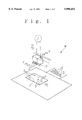
- FIG. 1 is a schematic perspective view illustrating an embodiment of an electronic component packaging unit adopting the method of packaging an electronic component of the present invention
- FIGS. 2(a) and 2(b) are descriptive view illustrating examples of a printed circuit board divided in the packaging method shown in FIG. 1;
- FIGS. 3(a) and 3(b) are descriptive views illustrating another embodiment of the reference origin shown in FIG. 1;
- FIG. 4 is a descriptive view illustrating an embodiment of the packaging method shown in FIG. 1;
- FIG. 5 is a descriptive view illustrating another configuration of the printed circuit board adopted in the method shown in FIG. 1;
- FIG. 6 is a descriptive view illustrating the relationship between the mechanical origin and the reference origin in the packaging method shown in FIG. 1;
- FIGS. 7(a) and 7(b) are descriptive view illustrating examples having different reference origins of areas in the packaging method shown in FIG. 1;
- FIGS. 8(a) and 8(b) are descriptive view illustrating another examples having different reference origins in the packaging method shown in FIG. 1;
- FIG. 9 is a descriptive view illustrating a conventional method of packaging an electronic component.
- the present invention having the construction as described above have the following functions.
- a printed circuit board placed on a packaging section is divided on control means into a plurality of areas, and a reference origin previously determined for each of the areas is entered into the control means.
- the individual reference origins provided on the printed circuit board are measured with detecting means, and the set origin value and the actual measured origin value are compared. When these set and measured values are different, the mounting origin coordinates are corrected through addition or subtraction of these values, and the result is entered into the control means.
- the electronic components received from the supply section are mounted for each area on the basis of the corrected origin for each area.
- An embodiment of the present invention comprises the steps, as shown in FIG. 1, of transferring electronic components b such as chip components or IC components received from the supply section n to a packaging section m, and mounting a prescribed number of such components onto appropriate positions on a printed circuit board c. Mounting at a prescribed position is accomplished by means of a packaging machine provided with a mounting head 2 movable in the X-axis and the Y-axis directions in accordance with a predetermined program entered into the control means 1 via a known computer.
- the mounting position is detected with detecting means 3 comprising a visual sensor such as a CCD camera, and the resultant signal is sent to the control means 1.
- the detected value is compared with a value of the previously set program for calculation, and when these values are different, correction is made in compliance with the difference.
- Packaging of the electronic component b in this embodiment of the present invention is accomplished through the steps of first dividing the printed circuit board c to be placed onto the packaging section m, for example, into a plurality of prescribed areas c1, c2, c3, c4, c5 and c6 as shown in FIGS. 2A and 2B on the control means 1, determining reference origins a1, a2, a3, a4, a5 and a6 for mounting an electronic component b for each of these areas c1, c2, c3, c4, c5 and c6, and previously setting the resultant values of coordinates in the control means 1.
- the number of areas c1, c2, . . . is set in response to the size and/or the extent of expansion/contraction of the printed circuit board c, or the mounting conditions of the electronic component b, and the board may be divided into more areas.
- the mounting head 2 is transferred to above the printed circuit board c, and the reference origins a1, a2, a3, a4, a5 and a6 for the individual areas c1, c2, c3, c4, c5 and c6 are measured with the detecting means 3.
- any of shapes recognizable by the CCD camera such as ⁇ , ⁇ , ⁇ and + may be selected.
- An origin may be marked by printing directly on the printed circuit board c, or a sharp corner of a circuit provided on the printed circuit board c as shown in FIG. 3A or a corner of an LSI lead pad on the printed circuit board c as shown in FIG. 3B may be employed.
- corrected origins for the areas c1, c2, c3, c4, c5 and c6 available from the control means 1, respectively, are calculated and set on the basis of the reference origins a1', a2', a3', a4', a5' and a6' resulting from the measurement.
- a deformation of the printed circuit board c is a material change brought about by an interior or exterior cause such as heat. Apart from a heat deformation, a deformation may be caused by the printed circuit board c itself, and in such a case, deformation is not always uniform throughout the entire surface of the printed circuit board c.
- the electronic component b is thus mounted on the packaging section m by controlling the mounting head 2 on the basis of this correction.
- the coordinates (X', Y') for the reference origin a1' on the packaging section m resulting from detection are compared with the coordinates (X, Y) for the reference origin on the packaging section m corresponding to the coordinates a1 for the reference origin on the printed circuit board c.
- the coordinates (X", Y") for the reference origin a1" on the packaging section m derived from detection are compared with the coordinates a1 (X, Y) for the reference origin on the packaging section m corresponding to the coordinates a1 of one of the reference origins on the printed circuit board c.
- the coordinates (X"', Y"') based on the reference origin a4"' on the packaging section m resulting from detection are compared with the coordinates (X4, Y4) based on the reference origin on the packaging section m corresponding to the coordinates a4 of one of the reference origins on the printed circuit board c.
- correction is made by adding the coordinates in the X and the Y directions (X"'-X4, Y"'-Y4) of the mounting position of the electronic component b based on the reference origin on the printed circuit board c in the area c4 to which the reference origin on the printed circuit board c in the program belongs.
- the coordinates (X"", Y”") based on the reference origin a4"" on the packaging section m resulting from detection are compared with the coordinates (X4, Y4) based on the reference origin on the packaging section m corresponding to the coordinates a4 of one of the reference origins on the printed circuit board c.
- correction is made by subtracting the mounting position of the electronic component b based on the reference origin on the printed circuit board c in the area to which the reference origin on the printed circuit board c in the program belongs.
- p is a mounting position of the electronic component b in the printed circuit board c, and the amount of deformation is uniform within the area c1. It is further assumed that the previously set mounting point p displaces by the same amount in the same direction.
- the printed circuit board c is placed at a prescribed position on the packaging section m so that the coordinates a1 (0, 0) of the reference origin of the divided area c1 on the printed circuit board c agree with the coordinates (40, 30) based on the reference origin on the packaging section m corresponding to the coordinates a1 (0, 0), i.e., so that the corner of the printed circuit board c takes coordinates (X-a, Y-b) based on the reference origin on the packaging section m.
- This a1 is expressed in mechanical coordinates, i.e., coordinates based on the reference origin on the packaging section m as a1(0+40, 0+30), i.e., a1(40, 30).
- the value of coordinates of the mounting point p i.e., the coordinates based on the reference origin on the printed circuit board take the value of p(20, 60), and this is expressed by mechanical coordinates of p as p(20+40, 60+30), hence p(60, 90).
- a1 and a1' are expressed as a(40, 30) and a1'(45, 40), respectively.
- the step of mounting the prescribed electronic component b is accomplished by controlling the mounting head 2 individually for each of the areas c1, c2, c3, c4, c5 and c6 with reference to the foregoing corrected origins for the areas c1, c2, c3, c4, c5 and c6.
- an actual mounting origin is determined by dividing a printed circuit board is divided into a plurality of areas, and carrying out measurement of reference origins provided for the individual areas, thereby determining an actual mounting origin on the basis of the data of such measurement. It is therefore possible to conduct a highly accurate numerical correction against a non-uniform deformation of the printed circuit board in the X and the Y directions, thus permitting mounting of an electronic component at a high accuracy.
- the correction is based on addition or subtraction of measured origin of coordinates and reference origins, an error in calculation can be inhibited to the slightest level.
- the correction is made through a simple operation comprising only an offset correction.
Landscapes
- Engineering & Computer Science (AREA)
- Manufacturing & Machinery (AREA)
- Microelectronics & Electronic Packaging (AREA)
- Operations Research (AREA)
- Supply And Installment Of Electrical Components (AREA)
Applications Claiming Priority (4)
| Application Number | Priority Date | Filing Date | Title |
|---|---|---|---|
| JP11331196 | 1996-05-08 | ||
| JP8-113311 | 1996-05-08 | ||
| JP9-098547 | 1997-04-16 | ||
| JP9098547A JPH1051198A (ja) | 1996-05-08 | 1997-04-16 | 電子部品実装方法 |
Publications (1)
| Publication Number | Publication Date |
|---|---|
| US5896652A true US5896652A (en) | 1999-04-27 |
Family
ID=26439695
Family Applications (1)
| Application Number | Title | Priority Date | Filing Date |
|---|---|---|---|
| US08/848,297 Expired - Fee Related US5896652A (en) | 1996-05-08 | 1997-04-29 | Method of packaging electronic components |
Country Status (3)
| Country | Link |
|---|---|
| US (1) | US5896652A (de) |
| EP (1) | EP0808092A2 (de) |
| JP (1) | JPH1051198A (de) |
Cited By (8)
| Publication number | Priority date | Publication date | Assignee | Title |
|---|---|---|---|---|
| US6141599A (en) * | 1996-07-16 | 2000-10-31 | Kabushiki Kaisha Shinkawa | Method for setting conveying data for a lead frame |
| US6397456B1 (en) * | 1996-10-14 | 2002-06-04 | Mydata Automation Ab | Method and a machine for automatic mounting of components and a pick-up head for such a machine |
| US6409642B2 (en) * | 1998-05-25 | 2002-06-25 | Sony Corporation | Assembling device |
| US6591486B1 (en) * | 1999-10-15 | 2003-07-15 | Data I/O Corporation | Manufacturing and carrier system with feeder/Programming/buffer system |
| US20080059329A1 (en) * | 2000-02-22 | 2008-03-06 | Luchene Andrew S V | Systems and methods wherein a transfer code facilitates a transaction between a seller and a buyer |
| US20080231905A1 (en) * | 2007-03-21 | 2008-09-25 | Industrial Technology Research Institute | Method for calculating ink-jet printing data |
| US7472737B1 (en) | 2003-01-15 | 2009-01-06 | Leannoux Properties Ag L.L.C. | Adjustable micro device feeder |
| US20150310161A1 (en) * | 2014-04-24 | 2015-10-29 | Nidec-Read Corporation | Method of designing circuit board inspecting jig, circuit board inspecting jig, and circuit board inspecting apparatus |
Families Citing this family (4)
| Publication number | Priority date | Publication date | Assignee | Title |
|---|---|---|---|---|
| SE516551C2 (sv) * | 1999-02-17 | 2002-01-29 | Ericsson Telefon Ab L M | Förfarande och anordning för precisionsmontering av en första apparatdel på en andra apparatdel |
| JP5040808B2 (ja) * | 2008-05-26 | 2012-10-03 | パナソニック株式会社 | 電子部品実装用装置および電子部品実装用作業実行方法 |
| JP2016174110A (ja) * | 2015-03-17 | 2016-09-29 | 東レエンジニアリング株式会社 | 実装位置補正方法および実装位置補正装置 |
| JP7436251B2 (ja) * | 2020-03-16 | 2024-02-21 | ファスフォードテクノロジ株式会社 | ダイボンディング装置および半導体装置の製造方法 |
Citations (16)
| Publication number | Priority date | Publication date | Assignee | Title |
|---|---|---|---|---|
| US4348276A (en) * | 1979-05-08 | 1982-09-07 | Tokyo Shibaura Denki Kabushiki Kaisha | Automatic testing apparatus for automatically testing a printed circuit board |
| JPS59107202A (ja) * | 1982-12-10 | 1984-06-21 | Matsushita Electric Ind Co Ltd | 微小部品装着位置検査装置 |
| FR2569935A1 (fr) * | 1984-08-31 | 1986-03-07 | Amaury Georges | Procede d'equipement de cartes a circuit imprime et machine pour la mise en oeuvre de ce procede |
| US4738025A (en) * | 1986-12-23 | 1988-04-19 | Northern Telecom Limited | Automated apparatus and method for positioning multicontact component |
| US4809430A (en) * | 1986-06-12 | 1989-03-07 | Matsushita Electric Industrial Co., Ltd. | Method and apparatus for mounting electronic parts |
| US4979290A (en) * | 1986-12-29 | 1990-12-25 | Kabushiki Kaisha Toshiba | Method for soldering electronic component |
| US5003692A (en) * | 1989-05-17 | 1991-04-02 | Matsushita Electric Industrial Co., Ltd. | Electric component mounting method |
| US5048178A (en) * | 1990-10-23 | 1991-09-17 | International Business Machines Corp. | Alignment--registration tool for fabricating multi-layer electronic packages |
| US5079834A (en) * | 1989-01-11 | 1992-01-14 | Hitachi, Ltd. | Apparatus for and method of mounting electronic components |
| US5379514A (en) * | 1992-11-19 | 1995-01-10 | Matsushita Electric Industrial Co., Ltd. | Electronic component installing apparatus and method |
| US5384956A (en) * | 1992-07-01 | 1995-01-31 | Yamaha Hatsudoki Kabushiki Kaisha | Method for mounting components |
| US5456003A (en) * | 1992-06-18 | 1995-10-10 | Matsushita Electric Industrial Co., Ltd. | Method for packaging a semiconductor device having projected electrodes |
| US5457880A (en) * | 1994-02-08 | 1995-10-17 | Digital Equipment Corporation | Embedded features for monitoring electronics assembly manufacturing processes |
| US5501005A (en) * | 1993-09-30 | 1996-03-26 | Matsushita Electric Industrial Co., Ltd. | Mounting device of electronic components and a mounting method |
| US5649356A (en) * | 1995-09-22 | 1997-07-22 | Universal Instruments Corporation | Method and apparatus for supplying and placing components |
| US5787577A (en) * | 1996-08-16 | 1998-08-04 | Motorola, Inc. | Method for adjusting an electronic part template |
-
1997
- 1997-04-16 JP JP9098547A patent/JPH1051198A/ja active Pending
- 1997-04-29 US US08/848,297 patent/US5896652A/en not_active Expired - Fee Related
- 1997-05-05 EP EP97107354A patent/EP0808092A2/de not_active Withdrawn
Patent Citations (17)
| Publication number | Priority date | Publication date | Assignee | Title |
|---|---|---|---|---|
| US4348276A (en) * | 1979-05-08 | 1982-09-07 | Tokyo Shibaura Denki Kabushiki Kaisha | Automatic testing apparatus for automatically testing a printed circuit board |
| JPS59107202A (ja) * | 1982-12-10 | 1984-06-21 | Matsushita Electric Ind Co Ltd | 微小部品装着位置検査装置 |
| FR2569935A1 (fr) * | 1984-08-31 | 1986-03-07 | Amaury Georges | Procede d'equipement de cartes a circuit imprime et machine pour la mise en oeuvre de ce procede |
| US4809430A (en) * | 1986-06-12 | 1989-03-07 | Matsushita Electric Industrial Co., Ltd. | Method and apparatus for mounting electronic parts |
| US4738025A (en) * | 1986-12-23 | 1988-04-19 | Northern Telecom Limited | Automated apparatus and method for positioning multicontact component |
| US4979290A (en) * | 1986-12-29 | 1990-12-25 | Kabushiki Kaisha Toshiba | Method for soldering electronic component |
| US5079834A (en) * | 1989-01-11 | 1992-01-14 | Hitachi, Ltd. | Apparatus for and method of mounting electronic components |
| US5003692A (en) * | 1989-05-17 | 1991-04-02 | Matsushita Electric Industrial Co., Ltd. | Electric component mounting method |
| US5048178A (en) * | 1990-10-23 | 1991-09-17 | International Business Machines Corp. | Alignment--registration tool for fabricating multi-layer electronic packages |
| US5456003A (en) * | 1992-06-18 | 1995-10-10 | Matsushita Electric Industrial Co., Ltd. | Method for packaging a semiconductor device having projected electrodes |
| US5384956A (en) * | 1992-07-01 | 1995-01-31 | Yamaha Hatsudoki Kabushiki Kaisha | Method for mounting components |
| US5379514A (en) * | 1992-11-19 | 1995-01-10 | Matsushita Electric Industrial Co., Ltd. | Electronic component installing apparatus and method |
| US5501005A (en) * | 1993-09-30 | 1996-03-26 | Matsushita Electric Industrial Co., Ltd. | Mounting device of electronic components and a mounting method |
| US5501005C1 (en) * | 1993-09-30 | 2002-05-28 | Matsushita Electric Industrial Co Ltd | Mounting device of electronic components and a mounting method |
| US5457880A (en) * | 1994-02-08 | 1995-10-17 | Digital Equipment Corporation | Embedded features for monitoring electronics assembly manufacturing processes |
| US5649356A (en) * | 1995-09-22 | 1997-07-22 | Universal Instruments Corporation | Method and apparatus for supplying and placing components |
| US5787577A (en) * | 1996-08-16 | 1998-08-04 | Motorola, Inc. | Method for adjusting an electronic part template |
Cited By (16)
| Publication number | Priority date | Publication date | Assignee | Title |
|---|---|---|---|---|
| US6141599A (en) * | 1996-07-16 | 2000-10-31 | Kabushiki Kaisha Shinkawa | Method for setting conveying data for a lead frame |
| US6397456B1 (en) * | 1996-10-14 | 2002-06-04 | Mydata Automation Ab | Method and a machine for automatic mounting of components and a pick-up head for such a machine |
| US6409642B2 (en) * | 1998-05-25 | 2002-06-25 | Sony Corporation | Assembling device |
| US6591486B1 (en) * | 1999-10-15 | 2003-07-15 | Data I/O Corporation | Manufacturing and carrier system with feeder/Programming/buffer system |
| US20030233749A1 (en) * | 1999-10-15 | 2003-12-25 | Data I/O Corporation | Manufacturing and carrier system with feeder/programming/buffer system |
| US6807727B2 (en) * | 1999-10-15 | 2004-10-26 | Data I/O Corporation | Manufacturing and carrier system with feeder/programming/buffer system |
| US20080059329A1 (en) * | 2000-02-22 | 2008-03-06 | Luchene Andrew S V | Systems and methods wherein a transfer code facilitates a transaction between a seller and a buyer |
| US7472737B1 (en) | 2003-01-15 | 2009-01-06 | Leannoux Properties Ag L.L.C. | Adjustable micro device feeder |
| US20090107638A1 (en) * | 2003-01-15 | 2009-04-30 | Leannoux Properties Ag L.L.C. | Adjustable Micro Device Feeder |
| US8079396B2 (en) | 2003-01-15 | 2011-12-20 | Leannoux Properties Ag L.L.C. | Adjustable micro device feeder |
| US20080231905A1 (en) * | 2007-03-21 | 2008-09-25 | Industrial Technology Research Institute | Method for calculating ink-jet printing data |
| US20150310161A1 (en) * | 2014-04-24 | 2015-10-29 | Nidec-Read Corporation | Method of designing circuit board inspecting jig, circuit board inspecting jig, and circuit board inspecting apparatus |
| KR20150123180A (ko) * | 2014-04-24 | 2015-11-03 | 니혼덴산리드가부시키가이샤 | 기판 검사 지그 설계 방법, 기판 검사 지그 및 기판 검사 장치 |
| CN105044392A (zh) * | 2014-04-24 | 2015-11-11 | 日本电产理德股份有限公司 | 基板检测夹具设计方法,基板检测夹具及基板检测装置 |
| TWI663682B (zh) * | 2014-04-24 | 2019-06-21 | 日商日本電產理德股份有限公司 | 基板檢測夾具設計方法,基板檢測夾具及基板檢測裝置 |
| CN105044392B (zh) * | 2014-04-24 | 2019-07-16 | 日本电产理德股份有限公司 | 基板检测夹具设计方法,基板检测夹具及基板检测装置 |
Also Published As
| Publication number | Publication date |
|---|---|
| JPH1051198A (ja) | 1998-02-20 |
| EP0808092A2 (de) | 1997-11-19 |
Similar Documents
| Publication | Publication Date | Title |
|---|---|---|
| JP3092809B2 (ja) | 検査方法、並びに検査プログラムデータの自動作成機能を有する検査装置 | |
| EP0808092A2 (de) | Methode zur Bestückung elektronischer Bauteile | |
| US4999764A (en) | Method of setting up apparatus for handling electrical or electronic components | |
| CN112318503B (zh) | 一种机器人校准系统和校准方法 | |
| US6710867B2 (en) | Device and method for inspecting a three-dimensional surface structure | |
| JP3500124B2 (ja) | 電気的な構成群の製作装置に設けられた保持装置の移動距離及び/又は角度位置を校正するための方法及び装置並びに校正基板 | |
| CN112147951B (zh) | 机加工设备热误差补偿方法及其装置、系统、介质、终端 | |
| US4922434A (en) | Linear interpolation for a component placement robot | |
| KR20010074993A (ko) | 기판 처리 방법 및 장치 | |
| CN1251256A (zh) | 一种制造电气部件的装置的测量方法和装置 | |
| KR0176662B1 (ko) | 칩마운터용 직교로봇의 칩마운팅 위치제어방법 및 위치제어장치 | |
| JP2793947B2 (ja) | 半田付け状態の外観検査方法 | |
| JP3334568B2 (ja) | 位置検出装置 | |
| KR100260490B1 (ko) | 부품실장기 및 그 실장방법 | |
| US20030193560A1 (en) | Precise position control apparatus and precise position control method using the same | |
| JPS6374530A (ja) | 部品の自動マウント方法 | |
| JP2000258121A (ja) | 複数カメラ校正用のマスター基板及び画像認識カメラの校正方法 | |
| JPS63133700A (ja) | 電子部品自動挿入機における部品挿入位置補正方法 | |
| JPH038400A (ja) | プリント基板の位置補正方法 | |
| JPH06190687A (ja) | 工作機械の熱変位補正装置 | |
| EP0326235A2 (de) | Verfahren zum Aufstellen einer Einrichtung zur Handhabung von elektrischen oder elektronischen Bauelementen | |
| JPH11168297A (ja) | 作業機での作業位置の判定方法と補正方法、それらを用いた作業機 | |
| KR100203329B1 (ko) | 포토센서를 이용한 기판의 틀어짐 보정방법 및 그 장치 | |
| JPS6230519B2 (de) | ||
| JPS63139679A (ja) | 部品搭載機 |
Legal Events
| Date | Code | Title | Description |
|---|---|---|---|
| AS | Assignment |
Owner name: TENRYU TECHNICS CO., LTD., JAPAN Free format text: ASSIGNMENT OF ASSIGNORS INTEREST;ASSIGNORS:TAGATA, GENICHI;UCHIDA, TOMIHIDE;REEL/FRAME:008991/0456 Effective date: 19970612 |
|
| AS | Assignment |
Owner name: TENRYU TECHNICS CO., LTD., JAPAN Free format text: CORRECTIVE ASSIGNMENT TO CORRECT ASSIGNEE'S ADDRESS AN ASSIGNMENT WAS PREVIOUSLY RECORDED ON REEL 8991 FRAME 0456;ASSIGNORS:TAGATA, GENICHI;UCHIDA, TOMIHIDE;REEL/FRAME:009354/0995 Effective date: 19970612 |
|
| REMI | Maintenance fee reminder mailed | ||
| LAPS | Lapse for failure to pay maintenance fees | ||
| LAPS | Lapse for failure to pay maintenance fees |
Free format text: PATENT EXPIRED FOR FAILURE TO PAY MAINTENANCE FEES (ORIGINAL EVENT CODE: EXP.); ENTITY STATUS OF PATENT OWNER: LARGE ENTITY |
|
| STCH | Information on status: patent discontinuation |
Free format text: PATENT EXPIRED DUE TO NONPAYMENT OF MAINTENANCE FEES UNDER 37 CFR 1.362 |
|
| FP | Lapsed due to failure to pay maintenance fee |
Effective date: 20030427 |