US5898416A - Display device - Google Patents
Display device Download PDFInfo
- Publication number
- US5898416A US5898416A US08/812,221 US81222197A US5898416A US 5898416 A US5898416 A US 5898416A US 81222197 A US81222197 A US 81222197A US 5898416 A US5898416 A US 5898416A
- Authority
- US
- United States
- Prior art keywords
- row
- electrodes
- display device
- rows
- supporting plate
- Prior art date
- Legal status (The legal status is an assumption and is not a legal conclusion. Google has not performed a legal analysis and makes no representation as to the accuracy of the status listed.)
- Expired - Fee Related
Links
- 229910021417 amorphous silicon Inorganic materials 0.000 claims description 2
- 239000000463 material Substances 0.000 description 6
- 239000004973 liquid crystal related substance Substances 0.000 description 5
- 230000005540 biological transmission Effects 0.000 description 2
- 238000010586 diagram Methods 0.000 description 2
- 238000005286 illumination Methods 0.000 description 2
- 230000010287 polarization Effects 0.000 description 2
- 239000000758 substrate Substances 0.000 description 2
- 239000004988 Nematic liquid crystal Substances 0.000 description 1
- 230000015556 catabolic process Effects 0.000 description 1
- 238000006731 degradation reaction Methods 0.000 description 1
- 230000001419 dependent effect Effects 0.000 description 1
- 230000000694 effects Effects 0.000 description 1
- 239000011521 glass Substances 0.000 description 1
- 239000011159 matrix material Substances 0.000 description 1
- 238000000034 method Methods 0.000 description 1
- 230000003287 optical effect Effects 0.000 description 1
Images


Classifications
-
- G—PHYSICS
- G09—EDUCATION; CRYPTOGRAPHY; DISPLAY; ADVERTISING; SEALS
- G09G—ARRANGEMENTS OR CIRCUITS FOR CONTROL OF INDICATING DEVICES USING STATIC MEANS TO PRESENT VARIABLE INFORMATION
- G09G3/00—Control arrangements or circuits, of interest only in connection with visual indicators other than cathode-ray tubes
- G09G3/20—Control arrangements or circuits, of interest only in connection with visual indicators other than cathode-ray tubes for presentation of an assembly of a number of characters, e.g. a page, by composing the assembly by combination of individual elements arranged in a matrix no fixed position being assigned to or needed to be assigned to the individual characters or partial characters
- G09G3/34—Control arrangements or circuits, of interest only in connection with visual indicators other than cathode-ray tubes for presentation of an assembly of a number of characters, e.g. a page, by composing the assembly by combination of individual elements arranged in a matrix no fixed position being assigned to or needed to be assigned to the individual characters or partial characters by control of light from an independent source
- G09G3/36—Control arrangements or circuits, of interest only in connection with visual indicators other than cathode-ray tubes for presentation of an assembly of a number of characters, e.g. a page, by composing the assembly by combination of individual elements arranged in a matrix no fixed position being assigned to or needed to be assigned to the individual characters or partial characters by control of light from an independent source using liquid crystals
- G09G3/3611—Control of matrices with row and column drivers
- G09G3/367—Control of matrices with row and column drivers with a nonlinear element in series with the liquid crystal cell, e.g. a diode, or M.I.M. element
-
- G—PHYSICS
- G09—EDUCATION; CRYPTOGRAPHY; DISPLAY; ADVERTISING; SEALS
- G09G—ARRANGEMENTS OR CIRCUITS FOR CONTROL OF INDICATING DEVICES USING STATIC MEANS TO PRESENT VARIABLE INFORMATION
- G09G2300/00—Aspects of the constitution of display devices
- G09G2300/08—Active matrix structure, i.e. with use of active elements, inclusive of non-linear two terminal elements, in the pixels together with light emitting or modulating elements
- G09G2300/088—Active matrix structure, i.e. with use of active elements, inclusive of non-linear two terminal elements, in the pixels together with light emitting or modulating elements using a non-linear two-terminal element
- G09G2300/0895—Active matrix structure, i.e. with use of active elements, inclusive of non-linear two terminal elements, in the pixels together with light emitting or modulating elements using a non-linear two-terminal element having more than one selection line for a two-terminal active matrix LCD, e.g. Lechner and D2R circuits
Definitions
- the invention relates to a display device comprising an electro-optical medium between a first supporting plate and a second supporting plate, which display device is provided with row electrodes on the first supporting plate and column electrodes on the second supporting plate.
- Such a display device can suitably be used, for example, to display alpha-numerical information and to display video information by means of passive electro-optical media such as liquid crystals, electrophoretic materials and electrochromic materials.
- a display device of the type mentioned in the opening paragraph is described in U.S. Pat. No. 5,151,691.
- Means for charging the pixel, prior to selection, to a voltage at the boundary of or beyond the range for picture display (also referred to as "resetting") are provided, comprising a distributed capacitance between the row electrode and the common electrode for each row of pixels.
- each common electrode is connected to a reference voltage via an additional diode to periodically recharge the capacitance.
- the charge stored in said capacitance for resetting must be large enough to supply the current necessary for resetting.
- the voltage drop across the pixel as a result of switching effects must be minimized.
- the width of the row electrode in U.S. Pat. No. 5,151,691 is approximately 1/15 of the height of a pixel. This is at the expense of the aperture (effective viewing area).
- the provision of the capacitance requires additional process steps, while recharging the capacitances requires an additional diode for each row of pixels.
- auxiliary row electrodes are mutually interconnected in groups of auxilliary row electrodes, each group having a common driving connection.
- row of pixels can be reset without the (distributed) capacitance being required.
- the external reset voltage can be chosen to be such that said additional diodes can be dispensed with. Since no (distributed) capacitance is required now, the width of the row electrodes (the dimension of the pixels remaining the same) can be smaller, resulting in a larger aperture. This has the advantage that the brightness increases while the power of an illumination source (of the type customary in this kind of display devices) remains the same, or the same brightness is obtained with less power. This has advantages, in particular, in display devices having a high-power illumination source, particularly if the picture diameters are larger than 40 cm, but also if the picture diameters are larger than, for example, 25 cm, an improvement is obtained.
- the number of mutually interconnected auxiliary row electrodes within a group, which are provided with a control voltage via the same common driving connection, can be chosen to be such (for example 10) that the number of additional external connections remains acceptable.
- FIG. 1 schematically shows an equivalent circuit diagram of a part of the device in accordance with the invention
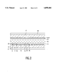
- FIG. 2 schematically shows, in section, a part of the device in accordance with the invention.
- FIGS. 3 to 6 show some control signals for a device in accordance with FIGS. 1 and 2.
- FIG. 1 schematically shows an electrical equivalent circuit diagram of a part of a display device 1.
- This device comprises a matrix of pixels 2 which are arranged in m rows and k columns.
- the pixels 2 are connected to row electrodes 5 via non-linear, two-pole switching elements, in this example diodes 3.
- a row of pixels is selected via the row electrodes 5, which select the relevant rows.
- the row electrodes are successively selected by means of a multiplex circuit 16.
- Incoming (video) information 7 is stored in a data register 9, if necessary after having been processed in a processing/control unit 8.
- the voltages supplied by the data register 9 to column electrodes 6 cover a voltage range which is sufficient to adjust the desired range of grey levels.
- the picture electrodes 14 form a common column electrode 6.
- the pixels 2 are further connected to an auxiliary row electrode 25 via non-linear, two-pole switching elements, in this example diodes 23.
- several electrodes 25 are mutually interconnected and connected to a common driving connection 24.
- FIG. 2 schematically shows, in cross-section, a part of a liquid-crystal display device 1 in accordance with the invention, which comprises a twisted-nematic liquid-crystal material 10 which is sandwiched between two substrates 4, 4', for example, of glass, which are provided with picture electrodes 13 and 14.
- Said picture electrodes 13 are connected on the one hand, via diodes 3 and via (schematically drawn) interconnections 15, to row electrodes 5 for supplying selection signals.
- the picture electrodes 14 are connected to column electrodes 6 which, in this example, are in the form of common, strip-shaped electrodes.
- the picture electrodes 13 on the first supporting plate 2 are connected on the other hand, via diodes 23 and interconnections 15, to (successive) auxiliary row electrodes 25 for supplying reset signals, a number of said electrodes 25 being mutually interconnected.
- the diodes are in this case made from amorphous silicon and may be, for example, pin diodes or Schottky diodes. Said diodes may be in the form of lateral diodes as described e.g. in U.S. Pat. No. 4,997,788 or ledge-diodes while, in addition, redundancy (for example two diodes arranged in series or in parallel) can be used.
- the device further comprises two polarizers 17, 18 having mutually perpendicular directions of polarization.
- the device also comprises orientation layers 11, 12, which orient the liquid-crystal material at the inner surfaces of the substrate, in this example, in the direction of the polarization axes of the polarizers, so that the cell has a twist angle of 90 degrees.
- the liquid-crystal material has a positive optical anisotropy and a positive dielectric anisotropy.
- FIGS. 3, 4, 5 and 6 show, in succession, the drive signals for resetting (connections 24) and selecting a single block, for example the first block of m' lines.
- the reset signal V reset has an amplitude which is sufficiently high to charge all pixels in the first m' rows to a voltage at the boundary of the voltage range for picture display or even beyond said range, irrespective of the voltage on the columns.
- the connection 24 of the relevant block acquires a voltage V nr .
- the first m' rows of pixels are reset again at the beginning of the next picture period (FIG. 3).
- a first row within a block is selected during a line period (or a part thereof) via a row electrode 5 by means of a selection voltage V s1 .
- the row electrode acquires a voltage V ns2 .
- the device is preferably operated by means of an AC voltage across the pixels.
- the data voltages in every subsequent picture period are presented in an inverted manner and, in the next picture period, row 1 is selected by means of a selection voltage V s2 (FIG. 4).
- FIG. 5 shows the selection signal for row 2; this is identical to that of row 1, yet shifted by a picture period plus a line period.
- the selection signal for row 3 is identical again to that for row 1 (FIG. 6), yet shifted by two line periods.
- the voltages across the pixels are presented with reversed sign (row inversion).
- dashed lines are used to indicate yet another variation of the selection voltages, with the row electrodes, after selection, first acquiring a non-selection voltage V ns1 via the voltage V s1 ; this is the minimum voltage necessary to preclude that the diodes 3 are conducting between the selection periods.
- m' can vary between 1/50 m and 1/200 m, depending on the required quality of the picture. For one display several values of m' may be used, e.g. in case different pictures are provided on one screen, while one of the pictures may be displayed with less quality than the other.
- the rows of pixels within one block are successively provided with the proper pixel voltage.
- the first row of each block retains this voltage (apart from leakage loss, etc.) during a period which is equal to a frame period minus the reset period (in the above example 1 line period), hence during (m-1) line periods, whereafter this row is selected again and provided with the proper information.
- the second row of each block retains the pixel voltage for a period equal to a frame period minus the reset period (1 line period) and 1 line period, in all (m-2) line periods, whereafter this row is selected again and provided with the proper information.
- the tenth row of each block retains the pixel voltage during a period which is equal to a frame period minus the reset period (1 line period) and 9 line periods, in all 10 line periods, whereafter this row is selected again and provided with the proper information.
- the row or column voltage within a block can advantageously be adapted for every subsequent selection of a row within said block, in such a manner that the transmission is adjusted so as to be slightly different.
- the amplitude of the column voltage during writing of the row selected as the second one is changed relative to the column voltage during writing of the row selected as the first row
- the column voltage during writing of the row selected as the third one is changed relative to the column voltage during writing of the row selected as the second row, etc.
- the invention provides a display device, which is based on a number of pixels which are arranged in rows and columns, each pixel having a two-pole switching element between an electrode of a pixel and a row electrode, and a second two-pole switching element between said electrode of the pixel and an auxiliary row electrode used for resetting, said auxiliary row electrode for resetting having a mutually common connection for a plurality of rows of pixels.
Landscapes
- Engineering & Computer Science (AREA)
- Chemical & Material Sciences (AREA)
- Crystallography & Structural Chemistry (AREA)
- Physics & Mathematics (AREA)
- Computer Hardware Design (AREA)
- General Physics & Mathematics (AREA)
- Theoretical Computer Science (AREA)
- Liquid Crystal (AREA)
- Devices For Indicating Variable Information By Combining Individual Elements (AREA)
- Liquid Crystal Display Device Control (AREA)
Applications Claiming Priority (2)
| Application Number | Priority Date | Filing Date | Title |
|---|---|---|---|
| EP96200744 | 1996-03-18 | ||
| EP96200744 | 1996-03-18 |
Publications (1)
| Publication Number | Publication Date |
|---|---|
| US5898416A true US5898416A (en) | 1999-04-27 |
Family
ID=8223791
Family Applications (1)
| Application Number | Title | Priority Date | Filing Date |
|---|---|---|---|
| US08/812,221 Expired - Fee Related US5898416A (en) | 1996-03-18 | 1997-03-06 | Display device |
Country Status (4)
| Country | Link |
|---|---|
| US (1) | US5898416A (fr) |
| EP (1) | EP0832479A1 (fr) |
| JP (1) | JPH11505635A (fr) |
| WO (1) | WO1997035298A2 (fr) |
Cited By (14)
| Publication number | Priority date | Publication date | Assignee | Title |
|---|---|---|---|---|
| US20020063661A1 (en) * | 2000-11-29 | 2002-05-30 | E Ink Corporation | Addressing schemes for electronic displays |
| US6421033B1 (en) * | 1999-09-30 | 2002-07-16 | Innovative Technology Licensing, Llc | Current-driven emissive display addressing and fabrication scheme |
| US20040054031A1 (en) * | 1996-07-19 | 2004-03-18 | E Ink Corporation | Electronically addressable microencapsulated ink and display thereof |
| US6825068B2 (en) | 2000-04-18 | 2004-11-30 | E Ink Corporation | Process for fabricating thin film transistors |
| US20050134554A1 (en) * | 2001-07-27 | 2005-06-23 | E Ink Corporation | Microencapsulated electrophoretic display with integrated driver |
| US20060139308A1 (en) * | 1995-07-20 | 2006-06-29 | E Ink Corporation | Addressing schemes for electronic displays |
| WO2006085241A1 (fr) * | 2005-02-14 | 2006-08-17 | Koninklijke Philips Electronics N.V. | Dispositifs a matrice active |
| US7176880B2 (en) | 1999-07-21 | 2007-02-13 | E Ink Corporation | Use of a storage capacitor to enhance the performance of an active matrix driven electronic display |
| US20070052757A1 (en) * | 1996-07-19 | 2007-03-08 | E Ink Corporation | Electronically addressable microencapsulated ink and display thereof |
| US20070222725A1 (en) * | 2006-03-24 | 2007-09-27 | Wintek Corporation | Structure and driving method for active photoelectric element |
| US7893435B2 (en) | 2000-04-18 | 2011-02-22 | E Ink Corporation | Flexible electronic circuits and displays including a backplane comprising a patterned metal foil having a plurality of apertures extending therethrough |
| US20140339400A1 (en) * | 2011-12-07 | 2014-11-20 | Sharp Kabushiki Kaisha | Method for operating optical sensor circuit, and method for operating display apparatus provided with optical sensor circuit |
| US9293511B2 (en) | 1998-07-08 | 2016-03-22 | E Ink Corporation | Methods for achieving improved color in microencapsulated electrophoretic devices |
| US10331005B2 (en) | 2002-10-16 | 2019-06-25 | E Ink Corporation | Electrophoretic displays |
Families Citing this family (14)
| Publication number | Priority date | Publication date | Assignee | Title |
|---|---|---|---|---|
| US7304634B2 (en) | 1995-07-20 | 2007-12-04 | E Ink Corporation | Rear electrode structures for electrophoretic displays |
| US7352353B2 (en) | 1995-07-20 | 2008-04-01 | E Ink Corporation | Electrostatically addressable electrophoretic display |
| US6710540B1 (en) | 1995-07-20 | 2004-03-23 | E Ink Corporation | Electrostatically-addressable electrophoretic display |
| US6664944B1 (en) | 1995-07-20 | 2003-12-16 | E-Ink Corporation | Rear electrode structures for electrophoretic displays |
| US7167155B1 (en) | 1995-07-20 | 2007-01-23 | E Ink Corporation | Color electrophoretic displays |
| US6839158B2 (en) | 1997-08-28 | 2005-01-04 | E Ink Corporation | Encapsulated electrophoretic displays having a monolayer of capsules and materials and methods for making the same |
| US6232950B1 (en) | 1997-08-28 | 2001-05-15 | E Ink Corporation | Rear electrode structures for displays |
| US6177921B1 (en) | 1997-08-28 | 2001-01-23 | E Ink Corporation | Printable electrode structures for displays |
| US7075502B1 (en) | 1998-04-10 | 2006-07-11 | E Ink Corporation | Full color reflective display with multichromatic sub-pixels |
| US7256766B2 (en) | 1998-08-27 | 2007-08-14 | E Ink Corporation | Electrophoretic display comprising optical biasing element |
| US6724519B1 (en) | 1998-12-21 | 2004-04-20 | E-Ink Corporation | Protective electrodes for electrophoretic displays |
| US6842657B1 (en) | 1999-04-09 | 2005-01-11 | E Ink Corporation | Reactive formation of dielectric layers and protection of organic layers in organic semiconductor device fabrication |
| US7030412B1 (en) | 1999-05-05 | 2006-04-18 | E Ink Corporation | Minimally-patterned semiconductor devices for display applications |
| US6900851B2 (en) | 2002-02-08 | 2005-05-31 | E Ink Corporation | Electro-optic displays and optical systems for addressing such displays |
Citations (4)
| Publication number | Priority date | Publication date | Assignee | Title |
|---|---|---|---|---|
| US4731610A (en) * | 1986-01-21 | 1988-03-15 | Ovonic Imaging Systems, Inc. | Balanced drive electronic matrix system and method of operating the same |
| US4997788A (en) * | 1987-10-19 | 1991-03-05 | U.S. Philips Corporation | Display device including lateral Schottky diodes |
| US5151691A (en) * | 1989-11-27 | 1992-09-29 | U.S. Philips Corporation | Active display device |
| US5666133A (en) * | 1991-12-13 | 1997-09-09 | Kyocera Corporation | Method for driving liquid crystal display unit |
-
1997
- 1997-02-26 JP JP9533289A patent/JPH11505635A/ja active Pending
- 1997-02-26 EP EP97902546A patent/EP0832479A1/fr not_active Withdrawn
- 1997-02-26 WO PCT/IB1997/000169 patent/WO1997035298A2/fr not_active Ceased
- 1997-03-06 US US08/812,221 patent/US5898416A/en not_active Expired - Fee Related
Patent Citations (4)
| Publication number | Priority date | Publication date | Assignee | Title |
|---|---|---|---|---|
| US4731610A (en) * | 1986-01-21 | 1988-03-15 | Ovonic Imaging Systems, Inc. | Balanced drive electronic matrix system and method of operating the same |
| US4997788A (en) * | 1987-10-19 | 1991-03-05 | U.S. Philips Corporation | Display device including lateral Schottky diodes |
| US5151691A (en) * | 1989-11-27 | 1992-09-29 | U.S. Philips Corporation | Active display device |
| US5666133A (en) * | 1991-12-13 | 1997-09-09 | Kyocera Corporation | Method for driving liquid crystal display unit |
Cited By (26)
| Publication number | Priority date | Publication date | Assignee | Title |
|---|---|---|---|---|
| US8139050B2 (en) | 1995-07-20 | 2012-03-20 | E Ink Corporation | Addressing schemes for electronic displays |
| US20090174651A1 (en) * | 1995-07-20 | 2009-07-09 | E Ink Corporation | Addressing schemes for electronic displays |
| US20060139308A1 (en) * | 1995-07-20 | 2006-06-29 | E Ink Corporation | Addressing schemes for electronic displays |
| US7148128B2 (en) | 1996-07-19 | 2006-12-12 | E Ink Corporation | Electronically addressable microencapsulated ink and display thereof |
| US20040054031A1 (en) * | 1996-07-19 | 2004-03-18 | E Ink Corporation | Electronically addressable microencapsulated ink and display thereof |
| US8035886B2 (en) | 1996-07-19 | 2011-10-11 | E Ink Corporation | Electronically addressable microencapsulated ink and display thereof |
| US20070057908A1 (en) * | 1996-07-19 | 2007-03-15 | E Ink Corporation | Electronically addressable microencapsulated ink and display thereof |
| US20070052757A1 (en) * | 1996-07-19 | 2007-03-08 | E Ink Corporation | Electronically addressable microencapsulated ink and display thereof |
| US9293511B2 (en) | 1998-07-08 | 2016-03-22 | E Ink Corporation | Methods for achieving improved color in microencapsulated electrophoretic devices |
| US7859637B2 (en) | 1999-07-21 | 2010-12-28 | E Ink Corporation | Use of a storage capacitor to enhance the performance of an active matrix driven electronic display |
| US7176880B2 (en) | 1999-07-21 | 2007-02-13 | E Ink Corporation | Use of a storage capacitor to enhance the performance of an active matrix driven electronic display |
| US6421033B1 (en) * | 1999-09-30 | 2002-07-16 | Innovative Technology Licensing, Llc | Current-driven emissive display addressing and fabrication scheme |
| US6825068B2 (en) | 2000-04-18 | 2004-11-30 | E Ink Corporation | Process for fabricating thin film transistors |
| US20050067656A1 (en) * | 2000-04-18 | 2005-03-31 | E Ink Corporation | Process for fabricating thin film transistors |
| US7365394B2 (en) | 2000-04-18 | 2008-04-29 | E Ink Corporation | Process for fabricating thin film transistors |
| US7893435B2 (en) | 2000-04-18 | 2011-02-22 | E Ink Corporation | Flexible electronic circuits and displays including a backplane comprising a patterned metal foil having a plurality of apertures extending therethrough |
| US20020063661A1 (en) * | 2000-11-29 | 2002-05-30 | E Ink Corporation | Addressing schemes for electronic displays |
| US7023420B2 (en) | 2000-11-29 | 2006-04-04 | E Ink Corporation | Electronic display with photo-addressing means |
| US20050134554A1 (en) * | 2001-07-27 | 2005-06-23 | E Ink Corporation | Microencapsulated electrophoretic display with integrated driver |
| US7382363B2 (en) | 2001-07-27 | 2008-06-03 | E Ink Corporation | Microencapsulated electrophoretic display with integrated driver |
| US10331005B2 (en) | 2002-10-16 | 2019-06-25 | E Ink Corporation | Electrophoretic displays |
| WO2006085241A1 (fr) * | 2005-02-14 | 2006-08-17 | Koninklijke Philips Electronics N.V. | Dispositifs a matrice active |
| US7629954B2 (en) * | 2006-03-24 | 2009-12-08 | Wintek Corporation | Structure and driving method for active photoelectric element |
| US20070222725A1 (en) * | 2006-03-24 | 2007-09-27 | Wintek Corporation | Structure and driving method for active photoelectric element |
| US20140339400A1 (en) * | 2011-12-07 | 2014-11-20 | Sharp Kabushiki Kaisha | Method for operating optical sensor circuit, and method for operating display apparatus provided with optical sensor circuit |
| US9488521B2 (en) * | 2011-12-07 | 2016-11-08 | Sharp Kabushiki Kaisha | Method for operating optical sensor circuit, and method for operating display apparatus provided with optical sensor circuit |
Also Published As
| Publication number | Publication date |
|---|---|
| JPH11505635A (ja) | 1999-05-21 |
| WO1997035298A3 (fr) | 1997-11-13 |
| WO1997035298A2 (fr) | 1997-09-25 |
| EP0832479A1 (fr) | 1998-04-01 |
Similar Documents
| Publication | Publication Date | Title |
|---|---|---|
| US5898416A (en) | Display device | |
| EP0299546B1 (fr) | Dispositif d'affichage et méthode de commande d'un tel dispositif | |
| EP0284134B1 (fr) | Méthode de commande d'un dispositif d'affichage à cristal liquide et dispositif d'affichage associé | |
| US5689282A (en) | Display device with compensation for stray capacitance | |
| KR0147917B1 (ko) | 전력 손실의 감소와 프레임 제어시의 수직 스트라이프 세이드의 감소를 도모한 액정 디스플레이 및 그의 제어 방법 | |
| US5781164A (en) | Matrix display systems | |
| US5838290A (en) | Display device with photovoltaic converter | |
| US4811006A (en) | Display arrangement with improved drive | |
| US5193018A (en) | Active matrix liquid crystal display system using complementary thin film transistors | |
| JP3248949B2 (ja) | マトリクス・ディスプレイ装置 | |
| US5767829A (en) | Liquid crystal display device including drive circuit for predetermining polarization state | |
| WO1990007768A1 (fr) | Systeme d'attaque d'affichage a cristaux liquides exempt de scintillement | |
| EP0324997B1 (fr) | Procédé permettant de commander un dispositif de reproduction | |
| EP0296663B1 (fr) | Dispositif d'affichage | |
| JPH04269792A (ja) | マトリクス表示装置の駆動方法及びこの方法で動作し得るマトリクス表示装置 | |
| JPS6327894A (ja) | 表示装置 | |
| US20030107544A1 (en) | Display devices and driving method therefor | |
| JPH02134618A (ja) | 表示装置 | |
| US6169531B1 (en) | Liquid-crystal control circuit display device with selection signal | |
| US4958152A (en) | Display device and method of driving such a device | |
| WO1997031359A2 (fr) | Dispositif d'affichage | |
| GB2217891A (en) | Matrix display device | |
| WO1996016392A1 (fr) | Circuit de correction destine a compenser des changements de parametres dans un affichage a matrice active |
Legal Events
| Date | Code | Title | Description |
|---|---|---|---|
| AS | Assignment |
Owner name: U.S. PHILIPS CORPORATION, NEW YORK Free format text: ASSIGNMENT OF ASSIGNORS INTEREST;ASSIGNORS:KUIJK, KAREL E.;OVERSLUIZEN, GERRIT;REEL/FRAME:009929/0903;SIGNING DATES FROM 19970206 TO 19970210 |
|
| REMI | Maintenance fee reminder mailed | ||
| LAPS | Lapse for failure to pay maintenance fees | ||
| STCH | Information on status: patent discontinuation |
Free format text: PATENT EXPIRED DUE TO NONPAYMENT OF MAINTENANCE FEES UNDER 37 CFR 1.362 |
|
| FP | Expired due to failure to pay maintenance fee |
Effective date: 20030427 |