US5900780A - Amplifier circuit for CMOS operational amplifier - Google Patents
Amplifier circuit for CMOS operational amplifier Download PDFInfo
- Publication number
- US5900780A US5900780A US08/692,275 US69227596A US5900780A US 5900780 A US5900780 A US 5900780A US 69227596 A US69227596 A US 69227596A US 5900780 A US5900780 A US 5900780A
- Authority
- US
- United States
- Prior art keywords
- voltage
- output
- node
- transistor
- current
- Prior art date
- Legal status (The legal status is an assumption and is not a legal conclusion. Google has not performed a legal analysis and makes no representation as to the accuracy of the status listed.)
- Expired - Lifetime
Links
Images

Classifications
-
- H—ELECTRICITY
- H03—ELECTRONIC CIRCUITRY
- H03F—AMPLIFIERS
- H03F3/00—Amplifiers with only discharge tubes or only semiconductor devices as amplifying elements
- H03F3/30—Single-ended push-pull [SEPP] amplifiers; Phase-splitters therefor
-
- H—ELECTRICITY
- H03—ELECTRONIC CIRCUITRY
- H03F—AMPLIFIERS
- H03F3/00—Amplifiers with only discharge tubes or only semiconductor devices as amplifying elements
- H03F3/45—Differential amplifiers
- H03F3/45071—Differential amplifiers with semiconductor devices only
- H03F3/45076—Differential amplifiers with semiconductor devices only characterised by the way of implementation of the active amplifying circuit in the differential amplifier
- H03F3/45179—Differential amplifiers with semiconductor devices only characterised by the way of implementation of the active amplifying circuit in the differential amplifier using MOSFET transistors as the active amplifying circuit
- H03F3/45183—Long tailed pairs
-
- H—ELECTRICITY
- H03—ELECTRONIC CIRCUITRY
- H03F—AMPLIFIERS
- H03F3/00—Amplifiers with only discharge tubes or only semiconductor devices as amplifying elements
- H03F3/30—Single-ended push-pull [SEPP] amplifiers; Phase-splitters therefor
- H03F3/3001—Single-ended push-pull [SEPP] amplifiers; Phase-splitters therefor with field-effect transistors
-
- H—ELECTRICITY
- H03—ELECTRONIC CIRCUITRY
- H03F—AMPLIFIERS
- H03F2203/00—Indexing scheme relating to amplifiers with only discharge tubes or only semiconductor devices as amplifying elements covered by H03F3/00
- H03F2203/30—Indexing scheme relating to single-ended push-pull [SEPP]; Phase-splitters therefor
- H03F2203/30021—A capacitor being coupled in a feedback circuit of a SEPP amplifier
Definitions
- the present invention relates to an amplifier circuit using a class-AB CMOS operational amplifier, in particular, an amplifier circuit suitable for use as an audio amplifier circuit for a portable telephone.
- An amplifier circuit using a class-AB CMOS amplifier has been widely utilized as an audio amplifier circuit, because of its various advantages as follows.
- the output current namely, the current consumed by the amplifier
- the current flowing through the loads connected to the output of the amplifier is determined according to the current flowing through the loads connected to the output of the amplifier.
- the amplifier has small distortion in the output waveform and relatively low current flows when no signal is applied to the amplifier.
- the amplifier features an output waveform with a small distortion and low power consumption during idle periods.
- the amplifier has a relatively high output drive capacity.
- the amplifier can provide an output having a relatively large voltage amplitude.
- the present invention has been created to solve the foregoing problems.
- An amplifier circuit comprises an output circuit having a p-type MOS transistor connected between a first power-voltage node and an output node, the gate electrode thereof being connected to a first input node, and an n-type MOS transistor connected between a ground-voltage node and the output node, the gate electrode thereof being connected to a second input node; a voltage-current conversion circuit having an inverted-input node to which an input signal is input and a non-inverted-input node to which a comparison or reference voltage is applied, the voltage-current conversion circuit outputting a value according to the voltage difference between the input signal and the comparison voltage; a signal conversion circuit for controlling the voltage of the second input node in the output circuit using as a reference a second specified voltage and also for controlling the voltage of the first input node in the output circuit using as a reference a first specified voltage, according to the output of the voltage-current conversion circuit; and a feedback circuit connected between the output node of the output circuit and the inverted-input node
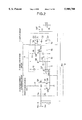
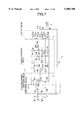
- FIG. 1 is a block diagram of an amplifier circuit showing a first embodiment of the present invention.
- FIG. 2 is a circuit diagram of an amplifier circuit shown in FIG. 1, using class AB-CMOS operational amplifier.
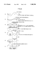
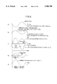
- FIGS. 3(a)-3(f) are diagrams showing the waveforms of the main sections in the first embodiment of the present invention.
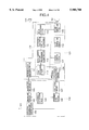
- FIG. 4 is a block diagram showing an embodiment of a semiconductor integrated circuit device for a portable telephone to which an embodiment of an amplifier circuit of the present invention is applied.
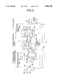
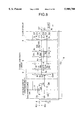
- FIG. 5 is a circuit diagram showing a second embodiment of the present invention.
- FIGS. 6(a)-6(e) are diagrams showing the waveforms of the main sections in the second embodiment of the present invention.
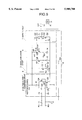
- FIG. 7 is a circuit diagram showing a third embodiment of the present invention.
- FIG. 8 is a circuit diagram showing a fourth embodiment of the present invention.
- FIG. 9 is a circuit diagram showing a fifth embodiment of the present invention.
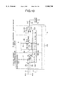
- FIG. 10 is a circuit diagram showing a sixth embodiment of the present invention.
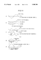
- FIGS. 11(a)-11(e) are diagrams showing the waveforms of the main sections in the sixth embodiment of the present invention.
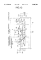
- FIG. 12 is a circuit diagram showing a seventh embodiment of the present invention.
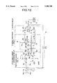
- FIG. 13 is a circuit diagram showing an eighth embodiment of the present invention.
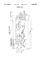
- FIG. 14 is a circuit diagram showing a ninth embodiment of the present invention.
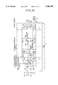
- FIG. 15 is a circuit diagram showing a tenth embodiment of the present invention.
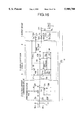
- FIG. 16 is a circuit diagram showing an eleventh embodiment of the present invention.
- FIGS. 1 and 2 are block and schematic diagrams of an amplifier circuit using a class-AB CMOS operational amplifier (hereinafter called op amp).
- op amp CMOS operational amplifier
- FIG. 1 an output circuit 1 for driving a load RL, such as a speaker or earphone, connected via capacitor C0 which is used for removing d.c. current.
- a load RL such as a speaker or earphone
- capacitor C0 which is used for removing d.c. current.
- the output circuit 1 comprises a first transistor Q1, e.g., a p-type MOS transistor, of which the gate electrode serving as a control electrode is connected to a first input node 1a, the source electrode serving as one main electrode is connected to a first power-voltage node to which a power voltage V DD (for example, 3 V in the first embodiment) is applied, and the drain electrode serving as the other main electrode is connected to an output node 1c.
- the output node 1c is the output OUT of the op amp.
- the output circuit 1 further includes a second transistor Q2, e.g., an n-type MOS transistor, of which the gate electrode serving as a control electrode is connected to a second input node 1b, the source electrode serving as one main electrode is connected to a ground-voltage node to which the ground voltage is applied, and the drain electrode serving as the other main electrode is connected to the output node 1c.
- a first capacitive component C1 such as a MOS capacitor, is connected between the control electrode and a main electrode connected to the output node 1c of the first transistor Q1, and a second capacitor C2, such as a MOS capacitor, is connected between the control electrode and a main electrode connected to the output node 1c of the second transistor Q2.
- the first and second capacitive components C1 and C2 are provided to adjust a phase shift between the signals input to the first input node 1a and the second input node 1b. For example, they are used for adjusting a phase of a system in order to prevent oscillation caused by signal composition of the output and inverted input, for example, when the output terminal and the inverted input terminal of the op amp are connected to configure a feedback circuit.
- a voltage-current conversion circuit 2 for outputting a value proportional to the voltage difference between the signal (the signal biased by V DD /2, i.e., half of the power voltage, V DD ) input to the inverted-input node 2a via an input resistor 6 from an inverted-input terminal IN(-) and the comparison or reference voltage (V DD /2, half of the power voltage, V DD ) specified by a comparison-voltage generating means 7 and input to a non-inverted-input node 2b connected to a non-inverted-input terminal IN(+).
- V DD the signal biased by V DD /2, i.e., half of the power voltage, V DD
- the voltage-current conversion circuit 2 controls the current flowing in transistors connected to the inverted-input node 2a and the non-inverted-input node 2b, and outputs current to the output node 2c according to the controlled current In other words, current flows from the output node 2c to an external circuit, or current flows from the external circuit into the output node 2c.
- the voltage-current conversion circuit 2 comprises a third transistor Q3, e.g., a p-type MOS transistor, of which the gate electrode serving as a control electrode is connected to the inverted-input node 2a, and a fourth transistor Q4, e.g., a p-type MOS transistor.
- the gate electrode of the fourth transistor Q4 serves as a control electrode and is connected to the non-inverted-input node 2b.
- the source electrode of the fourth transistor Q4 serves as one main electrode and is connected to the source electrode serving as one main electrode of the first transistor Q1.
- the drain electrode of the fourth transistor Q4 serves as the other main electrode is connected to an output node 2c.
- the fourth transistor Q4 is formed such that it has the same size as the third transistor Q3, namely, the same gate length and gate width to provide the same characteristics, and both transistors are configured as a pair of differential transistors.
- the voltage-current conversion circuit 2 also comprises a fifth transistor Q5, e.g., an n-type MOS transistor, of which the source electrode is connected to the ground voltage node, the drain electrode is connected to the drain electrode of the first transistor Q1, and the gate electrode serving as a control electrode is connected to the drain electrode.
- the voltage-current conversion circuit 2 further includes a sixth transistor Q6, e.g., an n-type transistor, of which the source electrode is connected to the second power-voltage node, the drain electrode is connected to the drain electrode of the fourth transistor Q4, and the gate electrode is connected to the control gate of the fifth transistor Q5.
- the fifth and sixth transistors Q5 and Q6 form a current mirror circuit.
- the sixth transistor Q6 is made such that it has the same size as the fifth transistor Q5, that is, the same gate length and same gate width to provide the same characteristics. The same current as that flowing through the fifth transistor Q5 flows through the sixth transistor Q6.
- a first constant-current power supply I1 for supplying constant current i1 to the third transistor Q3 and the fourth transistor Q4, with the first power voltage V DD being supplied from the power-voltage node.
- the first specified voltage is obtained by subtracting the gate-source voltage V GS1 (idle) of the first transistor Q1 from the power voltage V DD applied to the first power-voltage node, in the state when no input signal is applied. No input signal is applied when an input signal is not applied to the inverted-input terminal IN(-), current does not flow from the output terminal OUT to load RL connected to the output terminal OUT via capacitor C0 or vice verse, and the specified current I.sub.(idle) flows through the first and second transistors Q1 and Q2.
- the first specified voltage is used as a reference.
- the signal conversion circuit 3 is also for controlling the gate voltage of the second transistor Q2 in the output circuit 1 with the second specified voltage.
- the second specified voltage is the gate-source voltage V GS2 (idle) of the second transistor Q2 in the state when no signal is applied, which is lower than the first specified voltage, being used as a reference.
- the signal conversion circuit 3 receives the current flowing into the output node 2c of the voltage-current conversion circuit 2 and controls the current flowing into the first input node 1a and that flowing into the second input node 1b of the output circuit 1 and its corresponding voltages.
- the signal control circuit 3 comprises a first conversion section 4 for controlling the gate electrode of the first transistor Q1 in the output circuit 1, and a second conversion section 5 for controlling the gate electrode of the second transistor Q2 in the output circuit 1.
- the output voltage of the first conversion section 4 is generated according to that of the second conversion section 5.
- the first conversion section 4 has an input node 4a connected to the output node 2c of the voltage-current conversion circuit 2, and an output node 4b connected to the first input node 1a of the output circuit 1. According to the output of the voltage-current conversion circuit 2 (in this embodiment, it is also the output of the second conversion section 5), the conversion section 4 controls the gate electrode of the first transistor Q1 in the output circuit 1 with the first specified voltage being used as a reference. In other words, the first conversion section 4 controls the current flowing into the first input node 1a in the output circuit 1 and its corresponding voltage by controlling the flow of current to the output node 4b.
- the current flowing to the output node 4b is controlled according to the voltage of the input node 4a, which is controlled in accordance with the current flowing into the output node 2c of the voltage-current conversion circuit 2. That is, the current flowing from the output node 2c to the input node 4a or the current flowing from the input node 4a to the output node 2c is controlled by the first conversion section 4.
- the second conversion section 5 has an input node 5a connected to the output node 2c of the voltage-current conversion circuit 2, and an output node 5b connected to the second input node 1b of the output circuit 1. According to the output of the voltage-current conversion circuit 2, the conversion section 5 controls the gate electrode of the second transistor Q2 in the output circuit 1 with the second specified voltage being used as a reference. In other words, the conversion section 5 controls the current flowing into the first input node 1b in the output circuit 1 and its corresponding voltage, by controlling the flow of current to the output node 5b according to the voltage of the input node 5a, which is controlled in accordance with the current flowing into the output node 2c of the voltage-current conversion circuit 2. That is, the current flowing from the output node 2c to the input node 5a or the current flowing from the input node 5a to the output node 2c is controlled by the conversion section 5.
- FIG. 2 A detailed circuit of the signal conversion circuit 3 is shown in FIG. 2.
- a seventh transistor Q7 e.g. a p-type MOS transistor, of which the gate electrode is connected to the input node 4a, and the drain electrode is connected to the ground-voltage node, and a second constant-current power source I2 for supplying constant current i2 to a constant-current supply node, with the power voltage V DD being supplied from the first power-voltage node.
- the constant-current supply node is connected to the source electrode of the seventh transistor Q7.
- an eighth transistor Q8 e.g. an n-type MOS transistor, of which the gate electrode is connected to the connection point of the constant-current supply node of the second constant-current power source I2 and the source electrode of the seventh transistor Q7, and the drain electrode is connected to the first power-voltage node, and a third constant-current power source I3 for drawing constant current i3 to the ground-voltage node from a constant-current drawing node, which is connected to the source electrode of the eighth transistor Q8.
- the eighth transistor Q8 e.g. an n-type MOS transistor, of which the gate electrode is connected to the connection point of the constant-current supply node of the second constant-current power source I2 and the source electrode of the seventh transistor Q7, and the drain electrode is connected to the first power-voltage node, and a third constant-current power source I3 for drawing constant current i3 to the ground-voltage node from a constant-current drawing node, which is connected to the source electrode of the eighth transistor Q8.
- a load component R1 comprising a resistor component connected between the first power-voltage node and the output node 4b, and a ninth transistor Q9, e.g., an n-type MOS transistor, of which the drain electrode is connected to the load component R1.
- the specified bias voltage in this embodiment, the sum of the gate-source voltage, V GS2 (idle), of the second transistor Q2 and the gate-source voltage, V GS7 , of the seventh transistor Q7) is applied to the gate electrode of the ninth transistor Q9.
- a fourth constant-current power source I4 for drawing constant current i4 to the ground-voltage node from a constant-current drawing node which is connected to the source electrode of the ninth transistor Q9.
- a resistor component R2 connected between one main electrode of the eighth transistor Q8 and one main electrode of the ninth transistor Q9.
- Resistance r1 of load component R1 is specified such that the product of r1 and i4 equals the gate-source voltage, V GS1 (idle) of the first transistor Q1, obtained when no signal is applied.
- the first conversion section 4 of the signal conversion circuit 3 comprises the seventh transistor Q7, the second constant-current power source I2, the eighth transistor Q8, the third constant-current power source I3, load component R1, the ninth transistor Q9, the fourth constant-current power source I4, and resistor component R2.
- Wire 5c connects the input node 5a to the output node 5b.
- the current corresponding to the voltage at the input node 5a which is controlled by the current flowing into the output node 2c from input node 5a or the current flowing from the output node 2c to the input node 5a, flows across wire 5c to the output node 5b.
- the wire 5c is a part of the second conversion circuit 5, which controls the current flowing through the first input node 1b of the output circuit 1 and its corresponding voltage in the signal conversion circuit 3.
- the second conversion circuit 5 may be configured such that the input node 5a is also used as the output node 5b without using the wire 5c.
- FIG. 1 there is also shown a feedback circuit 8 connected between the output node 1c of the output circuit 1 and the non-inverted-input node 2a of the voltage-current conversion circuit 2. It is used for feeding back the voltage at the output node 1c in the output circuit 1 to the non-inverted-input node 2a in the voltage-current conversion circuit 2, and comprises another resistive component R3 as shown in FIG. 2, for example.
- a control circuit 9 which comprises the voltage-current conversion circuit 2 and the signal conversion circuit 3 controls the voltage at the second input node 1b with the second specified voltage being used as a reference, as well as the voltage at the first input node 1a of the output circuit 1 with the first specified voltage being used as a reference, according to the voltage difference between the signal input to the non-inverted-input terminal IN(-) and the comparison voltage output from the comparison-voltage generating means 7.
- the bias voltage, V DD /2 is applied to the inverted-input terminal IN(-), and the comparison voltage, V DD /2, is applied to the non-inverted-input terminal IN(+).
- the output node 5b which is directly connected to the input node 5a, is in the same state as the node 5a. Since the voltage at the output node 5b is set to the gate-source voltage, V GS2 (idle), of the second transistor Q2 at the state in which the specified current, I.sub.(idle), flows into the second transistor Q2, the second input node 1b of the output circuit 1 has a voltage of V GS2 (idle). This voltage is applied to the gate electrode of the second transistor Q2, the specified current, I.sub.(idle), flowing into the second transistor Q2.
- the second transistor Q2 is an n-type MOS transistor, it can operate in a slight conductivity state close to the non-conductivity state (the gate voltage is set to near the threshold voltage of the n-type MOS transistor), and the specified current can be very low current.
- the seventh transistor Q7 a p-type MOS transistor, of which the control electrode is connected to the input node 4a, becomes conductive since a low voltage of V GS2 (idle) is applied to the gate electrode. Constant current i2 flows into the seventh transistor Q7 from the second constant-current power source I2. As a result, the voltage of the gate electrode of the eighth transistor Q8 is higher than that of the gate electrode of the seventh transistor Q7 by the gate-source voltage of the seventh transistor Q7, V GS7 , that is, V GS2 (idle) +V GS7 .
- the magnitude ratio of the current flowing through the eighth transistor Q8 and that flowing through the ninth transistor Q9 is 1:n, as explained above.
- This voltage drop, i4 ⁇ r1 is set to the same voltage as the gate-source voltage, V GS1 (idle), of the first transistor Q1 in the state in which very low current I.sub.(idle) flows through the first transistor Q1 under a slight-conductivity state close to non-conductivity state (the gate voltage of the first transistor Q1, a p-type MOS transistor, is set to near the threshold voltage of the first transistor Q1).
- the voltage at the output node 4b is equal to the power voltage V DD applied to the power-voltage node minus i4 times r1
- the first transistor Q1 is a p-type MOS transistor, it can operate in a slight conductivity state close to the non-conductivity state, and the specified current can be very low current.
- the output nodes 5b and 4b of the signal conversion circuit 3 are maintained to be V GS2 (idle) and V DD -V GS1 (idle), respectively, when no signal is applied.
- V GS2 the voltage at the output node 2c of the voltage-current conversion circuit 2 becomes higher than V GS2 (idle)
- the voltages at the output nodes 5b and 4b are made higher to increase the conductivity level of the second transistor Q2, causing the current flowing through the second transistor Q2 to be higher than I.sub.(idle), and to reduce the conductivity level of the first transistor Q1, causing the current flowing through the first transistor Q1 to be lower than I.sub.(idle).
- the voltages at the output nodes 5b and 4b are made lower to reduce the conductivity level of the second transistor Q2, causing the current flowing through the second Q2 to be lower than I.sub.(idle), and to increase the conductivity level of the first transistor Q1, causing the current flowing through the first transistor Q1 to be higher than I.sub.(idle).
- the voltage at the output node 1c in the output circuit 1 is increased, the voltage at the non-inverted-input node 2a of the voltage-current conversion circuit 2 is increased, and the voltage of the output node 2c of the voltage-current conversion circuit 2 is increased, keeping the voltages at the output nodes 5b and 4b at V GS2 (idle) and V DD -V GS1 (idle), respectively.
- a current of i1/2+ ⁇ i1 flows into the fifth transistor Q5 and a current of i1/2+ ⁇ i1 also flows into the sixth transistor Q6, which forms the current mirror circuit together with the fifth transistor Q5.
- a current of i1/2- ⁇ i1 flows into the fourth transistor Q4 and a current of i1/2+ ⁇ i1 flows into the sixth transistor Q6. Then, a current of 2 ⁇ i1 flows into the sixth transistor Q6 from the input node 4a of the first conversion section 4 and the input node 5a of the second conversion section 5 of the signal conversion circuit 3.
- the voltage at the input node 4a of the first conversion section 4 and the input node 5a of the second conversion section 5 changes to a level lower than the gate-source voltage, V GS2 (idle), obtained when no signal is applied, of the second transistor Q2, according to the current difference 2 ⁇ i1.
- the voltage change at the input node 5a of the second conversion section 5 is the same as that at the output node 5b.
- the voltage, V GS2 , applied to the gate electrode of the second transistor Q2 is made lower than V GS2 (idle).
- the second transistor Q2 an n-type MOS transistor, is in a state which falls in the range from the non-conductivity state to a slight conductivity state close to the non-conductivity state.
- the current flowing through the second transistor Q2 is set to a value ranging from a level further lower than very low current I.sub.(idle) to 0 (see FIG. 3(d)).
- the seventh transistor Q7 which connects at its gate electrode to the input node 4a of the signal conversion circuit 3, remains conductive and constant current i2 continues flowing from the second constant-current power source I2, because a lower voltage than V GS2 (idle) is applied to the gate electrode.
- the voltage at the gate electrode of the eighth transistor Q8 becomes V GS2 +V GS7 , which is lower than V GS2 (idle) +V GS7 , because the voltage at the input node 4a is V GS2 , which is lower than V GS2 (idle).
- the voltage drop across load component R1 becomes large, making the voltage at the first input node 1a of the output circuit 1, that is, the gate voltage of the first transistor Q1, lower than V DD -V GS1 (idle) (see FIG. 3(d)).
- Voltage changes at the first and second input nodes 1a and 1b of the output circuit are negatively fed back to the non-inverted-input node 2a through capacitors C1 and C2 and feedback resistor R3 to stabilize the voltage at the non-inverted-input node 2a.
- FIG. 3(f) shows the current consumed in the output circuit 1.
- a current of i1/2- ⁇ i1 flows into the fifth transistor Q5 and a current of i1/2- ⁇ i1 also flows into the sixth transistor Q6, which forms the current mirror circuit together with the fifth transistor Q5.
- a current of i1/2+ ⁇ i1 flows into the fourth transistor Q4 and a current of i1/2- ⁇ i1 flows into the sixth transistor Q6. Then, a current of 2 ⁇ i1 flows from the fourth transistor Q4 into the input node 4a of the first conversion section 4 and the input node 5a of the second conversion section 5 of the signal conversion circuit 3.
- the voltage at the input node 4a of the first conversion section 4 and the input node 5a of the second conversion section 5 changes to a level higher than the gate-source voltage, V GS2 (idle), obtained when no signal is applied, of the second transistor Q2 according to the current difference 2 ⁇ i1.
- the voltage change at the input node 5a of the second conversion section 5 is the same as that at the output node 5b.
- the voltage applied to the gate electrode of the second transistor Q2 is made higher than V GS2 (idle).
- the second transistor Q2 an n-type MOS transistor, is then in a conductivity state which has a higher conductivity level than a slight conductivity state close to the non-conductivity state.
- the current flowing through the second transistor Q2 is set to a value higher than current I.sub.(idle) (see FIG. 3(d)).
- the seventh transistor Q7 which connects to the input node 4a at its gate electrode, remains conductive because a higher voltage applied to the gate electrode than V GS2 (idle) is not high enough to change the conductivity level, and constant current i2 continues flowing from the second constant-current power source I2.
- the voltage at the gate electrode of the eighth transistor Q8 becomes V GS2 +V GS7 , which is higher than V GS2 (idle) +V GS7 , because the voltage at the input node 4a is V GS2 , which is higher than V GS2 (idle).
- the gate voltage of the eighth transistor Q8 is higher than that (V GS2 (idle) +V GS7 ) of the ninth transistor Q9. More current (see FIG. 3(c)) than constant current i3 of the third constant-current power source I3 flows into the eighth transistor Q8, and less current (see FIG. 3(c)) than constant current i4 of the fourth constant-current power source I4 flows into the ninth transistor Q9. Current flows from the eighth transistor Q8 to the fourth constant-current power source I4 via resistive component R2.
- the voltage drop across load component R1 becomes small, making the voltage at the first input node 1a of the output circuit 1, that is, the gate voltage of the first transistor Q1, higher than V DD -V GS1 (idle) (see FIG. 3(d)).
- Voltage changes at the first and second input nodes 1a and 1b of the output circuit are negatively fed back to the non-inverted-input node 2a through capacitors C1 and C2 and feedback resistor R3 to stabilize the voltage at the non-inverted-input node 2a.
- FIG. 3(f) shows the current consumed in the output circuit 1.
- I.sub.(idle) flows when no signal is applied in order to obtain stable output waveform at the output node 1c
- I.sub.(idle) can be a stable and very low current since the p-type MOS transistor Q1 is connected between the power-voltage node and the output node 1c, and the n-type MOS transistor Q2 is connected between the output node 1c of the output circuit 1 and the ground node.
- the signal conversion circuit 3 receives the output of the voltage-current conversion circuit 2 comprising the differential amplifier circuit which receives the input signal, applies signals changing in phase to the gate electrode of the n-type MOS transistor Q2 and the gate electrode of the p-type MOS transistor Q1 according to the output of the circuit 2.
- the voltage appearing at the output node 1c is not influenced by the gate electrode of the first, p-type MOS transistor Q1 or the gate electrode of the second, n-type MOS transistor Q2.
- the amplitude can be stably obtained between the power voltage, V DD , applied to the power-voltage node and the ground voltage applied to the ground-voltage node.
- This lower limit corresponds to the voltage drop (50 mA ⁇ 6 ⁇ ) across the second, n-type MOS transistor Q2 (its "on” resistance is 6 ⁇ ) by the maximum current of 50 mA which is required to drive load RL, such as an earphone or a speaker, and flows into the second transistor Q2.
- the upper limit corresponds to the voltage obtained by subtracting from the power voltage V DD the voltage drop (50 mA ⁇ 6 ⁇ ) across the first, p-type MOS transistor Q1 (its "on” resistance is 6 ⁇ ) by the maximum current of 50 mA which is required to drive an earphone and speaker and flowing from the first transistor Q1.
- the receiving circuit for receiving and demodulated a signal according to a signal received by an antenna 101 and for outputting the sound signal to the earphone and speaker can be configured as one semiconductor integrated circuit device using MOS transistors.
- FIG. 4 there is shown the antenna 101, an earphone and speaker 102 serving as load RL, a microphone 103, a high-speed changeover switch 104 for selecting whether receiving a signal received by the antenna or sending a transmission signal to the antenna 101, a receiving circuit 105 for receiving, via the switch 104, the signal received by the antenna 101, a demodulating circuit 106 for demodulating the signal received by the receiving circuit, a modulating circuit 107 for modulating the signal based on the signal sent from the microphone 103, a transmission circuit 108 for outputting a transmission signal for sending the modulated signal of the modulating circuit 107 to the antenna 101 via the switch circuit 104, and a frequency synthesizer circuit 109 for controlling the receiving circuit 105 and the transmission circuit 108.
- a receiving circuit 105 for receiving, via the switch 104, the signal received by the antenna 101
- a demodulating circuit 106 for demodulating the signal received by the receiving circuit
- a modulating circuit 107 for modulating the signal based on the
- the modulating and demodulating circuit 110 can include the switch circuit 104, the receiving circuit 105, the demodulating circuit 106, the modulating circuit 107, the transmission circuit 108, and the frequency synthesizer circuit 109 formed as one semiconductor integrated circuit device comprising GaAs semiconductor substrate.
- a received-signal analyzing circuit 111 for receiving the demodulated signal from the demodulating circuit 106, a transmission-signal generating circuit 112 for outputting to the modulating circuit 107 by receiving and processing an analog signal based on the signal from the microphone 103, and a TDMA processing circuit 113 for outputting the digital signal by receiving and processing the signal processed in the received-signal analyzing circuit 111, and for outputting the analog signal to the transmission-signal generating circuit 112 by receiving and processing a digital signal based on a signal from the microphone 103.
- a data compression and enlargement circuit (ADPCM) 114 enlarges and outputs the digital signal processed in the TDMA processing circuit 113, and receives and compresses the digital signal based on the signal from the microphone 103 to output to the TDMA processing circuit 114.
- An A/D and D/A conversion circuit (PCMCODEC) 115 converts the enlarged signal from the data compression and enlargement circuit to the analog signal and outputs it, and converts the analog signal based on the signal from the microphone 103 to the digital signal and outputs it to the data compression and enlargement circuit 114.
- a sound processing circuit 116 for receiving and processing the analog signal converted in the A/D and D/A conversion circuit 115 to output to the sound amplifier circuit 100 comprising the amplifier circuit shown in FIGS. 1 and 2 as the input signal, and for receiving and processing the signal from the microphone 103 to output it to the A/D and D/A conversion circuit 115.
- a system control circuit (MCU) 117 for outputting control signals to control the received-signal analyzing circuit 111, the transmission-signal generating circuit 112, the TDMA processing circuit 113, the data compression and enlargement circuit 114, the A/D and D/A conversion circuit 115, the sound processing circuit 116, and the sound amplifier circuit 100, a clock generating circuit 118 for outputting clock signals to the received-signal analyzing circuit 111, the transmission-signal generating circuit 112, the TDMA processing circuit 113, the data compression and enlargement circuit 114, the A/D and D/A conversion circuit 115, the sound processing circuit 116, and the sound amplifier circuit 100.
- MCU system control circuit
- a receiving circuit 119 for receiving and processing the demodulated signal from the demodulating circuit 106 to output to the earphone or speaker 102 as a sound signal comprises the sound amplifier circuit 100 and the receiving-system circuit for processing the demodulated signal from the demodulating circuit 106 including the received-signal analyzing circuit 111, the TDMA processing circuit 113, the data compression and enlargement circuit 114, the A/D and D/A conversion circuit 115, and the sound processing circuit 116.
- a transmission circuit 120 for receiving and processing the signal from the microphone 103 to output the signal to be sent from the antenna 101 to the modulating circuit 107 comprises the transmission-system circuit for processing the signal from the microphone 103 including the transmission-signal generating circuit 112, the TDMA processing circuit 113, the data compression and enlargement circuit 114, the A/D and D/A conversion circuit 115, and the sound processing circuit 116.
- the receiving and transmission circuit 121 comprises the receiving circuit 119, the transmission circuit 120, the system control circuit 117, and the clock generating circuit 118.
- the receiving and transmission circuit 121 uses MOS transistors for all transistors and is formed as one semiconductor integrated circuit device using a silicon semiconductor substrate.
- FIG. 5 shows an amplifier circuit using a class-AB CMOS operational amplifier (hereinafter called op amp) according to a second embodiment of the present invention.
- the second embodiment differs from the first embodiment, shown in FIGS. 1 and 2, in that the power-voltage ranges for the voltage-current conversion circuit 2 and the signal conversion circuit 3 are greater than that for the output circuit 1, and consequently the circuit configuration of the signal conversion circuit 3 is slightly different. The other portions are the same.
- An output circuit 1 is connected between a ground-voltage node and a first power-voltage node to which a first power voltage V DD1 (in this embodiment, for example, 1.0 V) is applied.
- the output circuit 1 is driven by a power voltage of V DD and has the same detailed configuration as that described in the first embodiment.
- a voltage-current conversion circuit 2 is connected between the ground-voltage node and a second power-voltage node to which a second power voltage V DD2 (in this embodiment, for example, 2.5 V) which is higher than the first power voltage, V DD1 , is applied.
- the voltage-current conversion circuit 2 is driven by a power voltage of V DD2 and has the same detailed configuration as that described the first embodiment.
- a signal conversion circuit 3 is connected between the second power-voltage node and a third power-voltage node to which a negative voltage, V DD3 (in this embodiment, for example, -1.0 V), which is lower than the ground voltage, is applied.
- V DD3 negative voltage
- the signal conversion circuit 3 is driven by a power voltage of V DD2 -V DD3 , which has a greater power-voltage range than that of the output circuit 1, V DD1 , and that of the voltage-current conversion circuit 2, V DD2 .
- the signal conversion circuit 3 controls the gate voltage of the first transistor Q1 in the output circuit 1 with the first specified voltage (in this embodiment, the voltage obtained by subtracting the gate-source voltage V GS1 (idle) of the first transistor Q1, in the state when no input signal is applied, from the power voltage V DD1 applied to the first power-voltage node) being used as a reference, and controls the gate voltage of the second transistor Q2 in the output circuit 1 with the second specified voltage (in this embodiment, which is equal to the gate-source voltage V GS2 (idle) of the second transistor Q2 in the state when no signal is applied), which is lower than the first specified voltage, being used as a reference.
- the first specified voltage in this embodiment, the voltage obtained by subtracting the gate-source voltage V GS1 (idle) of the first transistor Q1, in the state when no input signal is applied, from the power voltage V DD1 applied to the first power-voltage node
- the second specified voltage in this embodiment, which is equal to the gate-source voltage V GS2
- the signal conversion circuit 3 comprises a first conversion section 4 for controlling the gate electrode of the first transistor Q1 in the output circuit 1, and a second conversion section 5, which is the same as that used in the first embodiment for controlling the gate electrode of the second transistor Q2 in the output circuit 1.
- the output voltage of the first conversion section 4 is generated according to that of the second conversion section 5.
- a first conversion section 4 comprises the 10th to 13th transistors Q10 to Q13, the fifth and sixth constant-current power sources I5 and I6, load component R1 and resistive component R4.
- the tenth transistor Q10 is a p-type MOS transistor in which the gate electrode serving as a control electrode is connected to the input node 4a.
- the fifth constant-current power source I5 supplies constant current i5 by receiving the second power voltage, V DD2 , from the second power-voltage node.
- the constant-current supply node is connected to the source electrode serving as one main electrode of the tenth transistor Q10.
- the eleventh transistor Q11 is an n-type MOS transistor in which the source electrode serving as one main electrode is connected to the third power-voltage node, and the drain electrode serving as the other main electrode and the gate electrode serving as a control electrode are connected to the drain electrode serving as one main electrode of the tenth transistor Q10.
- the twelfth transistor Q12 is a p-type MOS transistor in which the drain electrode serving as one main electrode is connected to the ground-voltage node, and the specified bias voltage is applied to the gate electrode serving as a control electrode.
- the sixth constant-current power source I6 supplies constant current i6 by receiving the second power voltage, V DD2 , from the second power-voltage node.
- the constant-current supply node is connected to the source electrode serving as one main electrode of the twelfth transistor Q12.
- the resistive component R4 is connected between one main electrode of the tenth transistor Q10 and one main electrode of the eleventh transistor Q11.
- Load component R1 is connected between the first power-voltage node and the output node 4b.
- the drain electrode serving as one main electrode is connected to the load component
- the gate electrode serving as a control electrode is connected to the control electrode of the eleventh transistor Q11
- the other main electrode is connected to the third power-voltage node.
- the thirteenth transistor Q13 forms a current mirror circuit together with the eleventh transistor Q11.
- the thirteenth transistor Q13 is formed such that it has the same size and the same characteristics as the eleventh transistor Q11 and the current having the same amplitude as the current flowing through the eleventh transistor Q11 flows through the thirteenth transistor Q13.
- Resistance r1 of the load component R1 is specified such that the product of r1 and i5 equals the gate-source voltage, V GS1 (idle), obtained when no signal is applied, of the first transistor Q1.
- power voltage V DD1 supplied to the first power-voltage node is supplied from, for example, one manganese dry cell or nickel-cadmium (Ni-Cd) dry cell
- the power voltages V DD2 and V DD3 supplied to the second and third power-voltage nodes are supplied from a DC-DC converter (not shown) for increasing and decreasing voltages, which is integrated with the amplifier circuit, by manipulating the power voltage supplied from, for example, one manganese dry cell or nickel-cadmium (Ni-Cd) dry cell.
- the desired operations can be obtained with no difficulty by directly supplying the power to the output circuit 1, which requires high current as drive current, and by supplying from the DC-DC converter or the like the power to the voltage-current conversion circuit 2 and the signal conversion circuit 3, which does not require high current.
- V DD /2 Since the same voltage, V DD /2, is applied to the inverted-input node 2a and the non-inverted-input node 2b of the voltage-current conversion circuit 2, the same voltage is applied to the gate electrodes of the third transistor Q3 and the fourth transistor Q4, causing the same current to flow through the third transistor Q3 and the fourth transistor Q4.
- the current is half of constant current i1 output from the first constant-current power source I1.
- the output node 5b which is directly connected to the input node 5a, is in the same state as the node 5a. Since the voltage at the output node 5b is set to the gate-source voltage, V GS2 (idle), of the second transistor Q2 at the state in which the specified current, I.sub.(idle), flows into the second transistor Q2, the second input node 1b of the output circuit 1 has a voltage of V GS2 (idle). This voltage is applied to the gate electrode of the second transistor Q2, the specified current, I.sub.(idle), flowing into the second transistor Q2.
- the second transistor Q2 is an n-type MOS transistor, it can operate in a slight conductivity state close to the non-conductivity state (the gate voltage is set to near the threshold voltage of the n-type MOS transistor), and the specified current can be very low current.
- a low voltage of V GS2 (idle) is applied to the gate electrode of the tenth transistor Q10, a p-type MOS transistor of which the gate electrode is connected to the input node 4a.
- the specified bias voltage is applied to the gate electrode of the twelfth transistor Q12, which forms a differential pair together with the tenth transistor Q10. Since substantially the same voltage is applied to the gate electrodes of the tenth and twelfth transistors Q10 and Q12 in this case, the magnitude ratio of the current flowing through the tenth transistor Q10 and that flowing through the twelfth transistor Q12 is 1:n.
- This voltage drop, i5 ⁇ r1 is set to the same voltage as the gate-source voltage, V GS1 (idle), of the first transistor Q1 in the state in which very low current I.sub.(idle) flows through the first transistor Q1 under a slight-conductivity state close to non-conductivity state (the gate voltage of the first transistor Q1, a p-type OS transistor, is set to near the threshold voltage of the first transistor Q1).
- the specified current, I.sub.(idle) flows into the first transistor Q1. Since the first transistor Q1 is a p-type MOS transistor, it can operate in a slight conductivity state close to the non-conductivity state, and the specified current can be very low current.
- the output nodes 5b and 4b of the signal conversion circuit 3 are maintained to be V GS2 (idle) and V DD -V GS1 (idle), respectively, when no signal is applied. That is, when the voltage at the output node 2c of the voltage-current conversion circuit 2 becomes higher than V GS2 (idle), the voltages at the output nodes 5b and 4b are made higher to increase the conductivity level of the second transistor Q2.
- the voltage at the non-inverted-input node 2a of the voltage-current conversion circuit 2 is increased, and the voltage of the output node 2c of the voltage-current conversion circuit 2 is increased, keeping the voltages at the output nodes 5b and 4b at V GS2 (idle) and V DD -V GS1 (idle), respectively.
- a current of i1/2+ ⁇ i1 flows into the fifth transistor Q5 and a current of i1/2+ ⁇ i1 also flows into the sixth transistor Q6, which forms the current mirror circuit together with the fifth transistor Q5.
- a current of i1/2- ⁇ i1 flows into the fourth transistor Q4 and a current of i1/2+ ⁇ i1 flows into the sixth transistor Q6. Then, a current of 2 ⁇ i1 flows into the sixth transistor Q6 from the input node 4a of the first conversion section 4 and the input node 5a of the second conversion section 5 of the signal conversion circuit 3.
- the voltage at the input node 4a of the first conversion section 4 and the input node 5a of the second conversion section 5 changes to a level lower than the gate-source voltage, V GS2 (idle), obtained when no signal is applied, of the second transistor Q2, according to the current difference 2 ⁇ i1.
- the voltage change at the input node 5a of the second conversion section 5 is the same as that at the output node 5b.
- the voltage, V GS2 , applied to the gate electrode of the second transistor Q2 is made lower than V GS2 (idle).
- the second transistor Q2 an n-type MOS transistor, is in a state which falls in the range from the non-conductivity state to a slight conductivity state close to the non-conductivity state.
- the current flowing through the second transistor Q2 is set to a value ranging from a level further lower than very low current I.sub.(idle) to 0 (see FIG. 6(c)).
- a lower voltage than V GS2 (idle) is applied to the gate electrode of the tenth transistor Q10, which is connected to the input node 4a at the gate electrode. According to the voltage difference, the conductivity level of the tenth transistor Q10 is higher than that of the twelfth transistor Q12.
- a current of i5+ ⁇ i flows into the tenth transistor Q10, and a current of i6- ⁇ i flows into the twelfth transistor Q12, where ⁇ i1 is a current increment increasing or decreasing depending on the voltage difference. It flows into the tenth transistor Q10 through resistive component R4 from the sixth constant-current power source I6.
- the voltage drop across load component R1 becomes large, making the voltage at the first input node 1a of the output circuit 1, that is the gate voltage of the first transistor Q1, lower than V DD -V GS1 (idle) (see FIG. 6(c)).
- the voltage (output signal) at the output node 1c of the output circuit 1 becomes higher than V DD /2 (see FIG. 6(c)).
- Voltage changes at the first and second input nodes 1a and 1b of the output circuit are negatively fed back to the non-inverted-input node 2a through capacitors C1 and C2 and feedback resistor R3 to stabilize the voltage at the non-inverted-input node 2a.
- FIG. 6(e) shows the current consumed in the output circuit 1.
- a current of i1/2- ⁇ i1 flows into the fifth transistor Q5 and a current of i1/2- ⁇ i1 also flows into the sixth transistor Q6, which forms the current mirror circuit together with the fifth transistor Q5.
- a current of i1/2+ ⁇ i1 flows into the fourth transistor Q4 and a current of i1/2- ⁇ i1 flows into the sixth transistor Q6. Then, a current of 2 ⁇ i1 flows from the fourth transistor Q4 into the input node 4a of the first conversion section 4 and the input node 5a of the second conversion section 5 in the signal conversion circuit 3.
- the voltage at the input node 4a of the first conversion section 4 and the input node 5a of the second conversion section 5 changes to a level higher than the gate-source voltage, V GS2 (idle), obtained when no signal is applied, of the second transistor Q2, according to the current difference 2 ⁇ i1.
- the voltage change at the input node 5a of the second conversion section 5 is the same as that at the output node 5b.
- the voltage applied to the gate electrode of the second transistor Q2 is made higher than V GS2 (idle).
- the second transistor Q2 an n-type MOS transistor, is in a state which has higher conductivity than a slight conductivity state close to the non-conductivity state.
- the current flowing through the second transistor Q2 is set to a value higher than current I.sub.(idle) (see FIG. 6(c)).
- a lower voltage than V GS2 (idle) is applied to the gate electrode of the tenth transistor Q10, which is connected to the input node 4a at the gate electrode. According to the voltage difference, the conductivity level of the tenth transistor Q10 is lower than that of the twelfth transistor Q12.
- a current of i5- ⁇ i flows into the tenth transistor Q10, and a current of i6+ ⁇ i flows into the twelfth transistor Q12, where ⁇ i1 is a current increment increasing or decreasing depending on the voltage difference. It flows into the twelfth transistor Q12 through resistive component R4 from the fifth constant-current power source I6.
- the voltage drop across load component R1 becomes small, making the voltage at the first input node 1a of the output circuit 1, that is, the gate voltage of the first transistor Q1, higher than V DD -V GS1 (idle) (see FIG. 6(c)).
- the voltage (output signal) at the output node 1c of the output circuit 1 becomes lower than V DD /2 (see FIG. 6(c)).
- Voltage changes at the first and second input nodes 1a and 1b of the output circuit are negatively fed back to the non-inverted-input node 2a through capacitors C1 and C2 and feedback resistor R3 to stabilize the voltage at the non-inverted-input node 2a.
- FIG. 6(e) shows the current consumed in the output circuit 1.
- An amplifier circuit using the op amp having the structure described above has the same advantages as described in the first embodiment.
- the power-voltage range of the signal conversion circuit 3 is wider than that of the output circuit 1, the gate-voltage amplitudes of the first and second transistors Q1 and Q2 which constitute the output circuit 1 can be set large, and the operation resistance of the first and second transistors Q1 and Q2 can be sufficiently reduced.
- FIG. 7 shows an amplifier circuit using a class-AB CMOS operational amplifier according to a third embodiment of the present invention.
- the third embodiment differs from the first embodiment, shown in FIGS. 1 and 2, in that the circuit configuration of the signal conversion circuit 3 is different. The other portions are the same.
- a signal conversion circuit 3 controls the gate voltage of the first transistor Q1 in the output circuit 1 with the first specified voltage being used as a reference, and controls the gate voltage of the second transistor Q2 in the output circuit 1 with the second specified voltage, which is lower than the first specified voltage, being used as a reference.
- the first specified voltage is obtained by subtracting the gate-source voltage, V GS1 (idle), of the first transistor Q1 in the state when no input signal is applied from the power voltage, V DD1 , applied to the first power-voltage node.
- the second specified voltage is equal to the gate-source voltage, V GS2 (idle), of the second transistor Q2 in the state when no signal is applied.
- the signal conversion circuit 3 comprises a first conversion section 4 which is the similar to that used in the first embodiment for controlling the gate voltage of the first transistor Q1 in the output circuit 1, and a second conversion section 5 which is different from that used in the first embodiment for controlling the gate voltage of the second transistor Q2 in the output circuit 1.
- the first conversion section 4 is the same as that of the first embodiment described above except that the seventh transistor Q7 and the second constant-current power source I2 are removed and the input node 4a connected to the output node 2c of the voltage-current conversion circuit 2 is directly connected to the gate electrode of the eighth transistor Q8.
- the bias voltage applied to the gate electrode of the ninth transistor Q9 can be set to any value.
- the bias voltage is set to the same value as the voltage at the output node 2c of the voltage-current conversion circuit 2, obtained when no signal is applied.
- V DD the power voltage
- the bias voltage is set to the same value, V DD /2, increasing design margin.
- the second conversion section 5 comprises the fourteenth and fifteenth transistors Q14 and Q15, the seventh and eighth constant-current power sources I7 and I8, load component R5 and the resistive component R6.
- the fourteenth transistor Q14 is a p-type MOS transistor in which the gate electrode serving as a control electrode is connected to the input node 5a which is connected to the output node 2c of the voltage-current conversion circuit 2 and the drain electrode serving as one main electrode is connected to the ground node.
- the seventh constant-current power source I7 supplies constant current i7 by receiving the power voltage, V DD , from the power-voltage node.
- the constant-current supply node is connected to the source electrode serving as one main electrode of the fourteenth transistor Q14.
- the fifteenth transistor Q15 is a p-type MOS transistor in which the drain electrode serving as one main electrode is connected to the output node 5b.
- the output node 5b is connected to the second input node of the output circuit 1, and the specified bias voltage is applied to the gate electrode serving as a control electrode.
- the specified bias voltage is the same as the voltage at the output node 2c in the voltage-current conversion circuit 2 with no signal being applied and the same as the bias voltage applied to the gate electrode of the ninth transistor Q9.
- the eighth constant-current power source I8 supplies constant current i8 by receiving the power voltage, V DD , from the power-voltage node.
- the constant-current supply node is connected to the source electrode serving as one main electrode of the fifteenth transistor Q15.
- Load component R5 is a resistive component connected between the ground node and the output node 5b.
- the resistive component R6 is connected between one main electrode of the fourteenth transistor Q14 and one main electrode of the fifteenth transistor Q15.
- Resistance r5 of the load component R5 is specified such that the product of r5 and i8 equals the gate-source voltage, V GS2 (idle), of the second transistor Q2 with no signal being applied.
- a third capacitive component C3, such as a MOS capacitor, is connected between the output node 2c of the voltage-current conversion circuit 2 and the output node 1c of the output circuit 1. It is used for eliminating a phase shift between the output node 2c of the voltage-current conversion circuit 2 and the output node 1c of the output circuit 1.
- V DD /2 Since the same voltage, V DD /2, is applied to the inverted-input node 2a and the non-inverted-input node 2b of the voltage-current conversion circuit 2, the same voltage is applied to the gate electrodes of the third transistor Q3 and the fourth transistor Q4, causing the same current to flow through the third transistor Q3 and the fourth transistor Q4.
- the current is half of constant current i1 output from the first constant-current power source I1.
- the voltage at the output node 2c of the voltage-current conversion circuit 2 in this case is set such that it equals the bias voltage applied to the gate electrodes of the ninth and fifteenth transistors Q9 and Q15.
- the gate voltage of the fourteenth transistor Q14 is the same as that of the fifteenth transistor Q15, therefore, both of which form a differential pair of transistors in the second conversion section 5, the ratio of the amount of current flowing through the fourteenth transistor Q14 to that of current flowing through the fifteenth transistor Q15 is 1:m.
- the second transistor Q2 is an n-type MOS transistor, it can operate in a slight conductivity state close to the non-conductivity state (the gate voltage is set to near the threshold voltage of the n-type MOS transistor), and the specified current can be very low current.
- the gate voltage of the eighth transistor Q8 is the same as that of the ninth transistor Q9, both of which form a differential pair of transistors in the first conversion section 4, the ratio of the amount of current flowing through the eighth transistor Q8 to that of current flowing through the ninth transistor Q9 is 1:n.
- This voltage drop, i4 ⁇ r1 is set to the same voltage as the gate-source voltage, V GS1 (idle), of the first transistor Q1 in the state in which very low current, I.sub.(idle), flows through the first transistor Q1 under a slight-conductivity state close to non-conductivity state (the gate voltage of the first transistor Q1, a p-type MOS transistor, is set to near the threshold voltage of the first transistor Q1).
- the specified current, I.sub.(idle) flows into the first transistor Q1. Since the first transistor Q1 is a p-type MOS transistor, it can operate in a slight conductivity state close to the non-conductivity state, and the specified current can be very low current.
- the output nodes 5b and 4b of the signal conversion circuit 3 are maintained to be V GS2 (idle) and V DD -V GS1 (idle), respectively, when no signal is applied.
- V GS2 the voltages at the output nodes 5b and 4b are made higher to increase the conductivity level of the second transistor Q2, making the current flowing through Q2 higher than I.sub.(idle), and to reduce the conductivity level of the first transistor Q1, making the current flowing through Q1 lower than I.sub.(idle), thereby the voltage at the output node 1c in the output circuit 1 is reduced, the voltage at the non-inverted-input node 2a of the voltage-current conversion circuit 2 is reduced, and the voltage of the output node 2c of the voltage-current conversion circuit 2 is reduced, keeping the voltages at the output nodes 5b and 4b at V GS2
- the voltages at the output nodes 5b and 4b are made lower to reduce the conductivity level of the second transistor Q2, making the current flowing through Q2 lower than I.sub.(idle), and to increase the conductivity level of the first transistor Q1, making the current flowing through Q1 higher than I.sub.(idle), thereby the voltage at the output node 1c in the output circuit 1 is increased, the voltage at the non-inverted-input node 2a of the voltage-current conversion circuit 2 is increased, and the voltage of the output node 2c of the voltage-current conversion circuit 2 is increased, keeping the voltages at the output nodes 5b and 4b at V GS2 (idle) and V DD -V GS1 (idle), respectively.
- a current of i1/2+ ⁇ i1 flows into the fifth transistor Q5 and a current of i1/2+ ⁇ i1 also flows into the sixth transistor Q6, which forms the current mirror circuit together with the fifth transistor Q5.
- a current of i1/2- ⁇ i1 flows into the fourth transistor Q4 and a current of i1/2+ ⁇ i1 flows into the sixth transistor Q6. Then, a current of 2 ⁇ i1 flows into the sixth transistor Q6 from the input node 4a of the first conversion section 4 and the input node 5a of the second conversion section 5 of the signal conversion circuit 3.
- the voltage at the input node 4a of the first conversion section 4 and the input node 5a of the second conversion section 5 changes to a level lower than the bias voltage (in the third embodiment, V DD /2) applied to the ninth and fifteenth transistors Q9 and Q15 according to the current difference 2 ⁇ i1.
- the conductivity level of the fourteenth transistor Q14 is higher than that of the fifteenth transistor Q15 according to this voltage difference.
- a current of i7+ ⁇ i flows into the fourteenth transistor Q14, and a current of i8- ⁇ i flows into the fifteenth transistor Q15, where ⁇ i is a current increment increasing or decreasing depending on the voltage difference and flows into the fourteenth transistor Q14 through resistive component R6 from the eighth constant-current power source I8.
- the voltage drop across load component R5 is reduced.
- the voltage at the second input node 1b of the output circuit 1, namely, the gate voltage, V GS2 , of the second transistor Q2 is lower than V GS2 (idle).
- the second transistor Q2, an n-type MOS transistor, is in a state which falls in the range from the non-conductivity state to a slight conductivity state close to the non-conductivity state.
- the current flowing through the second transistor Q2 is set to a value ranging from a level further lower than very low current I.sub.(idle) to 0.
- a lower voltage than V DD /2 is applied to the gate electrode of the eighth transistor Q8, which is connected to the input node 4a at the gate electrode. According to the voltage difference, the conductivity level of the eighth transistor Q8 is lower than that of the ninth transistor Q9.
- a current of i3- ⁇ i flows into the eighth transistor Q8, and a current of i4+ ⁇ i flows into the ninth transistor Q9, where ⁇ i1 is a current increment increasing or decreasing depending on the voltage difference and flows into the third constant-current power source I3 through resistive component R2 from the ninth transistor Q9.
- the voltage drop across load component R1 becomes large, making the voltage at the first input node 1a of the output circuit 1, that is, the gate voltage of the first transistor Q1, lower than V DD -V GS1 (idle).
- the conductivity level of the first transistor Q1, a p-type MOS transistor, becomes high, and the current flowing through the first transistor Q1 becomes higher than I.sub.(idle).
- the voltage (output signal) at the output node 1c of the output circuit 1 becomes higher than V DD /2.
- Voltage changes at the first and second input nodes 1a and 1b of the output circuit 1 and a voltage change at the output node 2c of the voltage-current conversion circuit 2 are negatively fed back to the non-inverted-input node 2a through capacitors C1, C2, and C3 and feedback resistor R3 to stabilize the voltage at the non-inverted-input node 2a.
- a current of i1/2- ⁇ i1 flows into the fifth transistor Q5 and a current of i1/2- ⁇ i1 also flows into the sixth transistor Q6, which forms the current mirror circuit together with the fifth transistor Q5.
- a current of i1/2+ ⁇ i1 flows into the fourth transistor Q4 and a current of i1/2- ⁇ i1 flows into the sixth transistor Q6. Then, a current of 2 ⁇ i1 flows from the fourth transistor Q4 into the input node 4a of the first conversion section 4 and the input node 5a of the second conversion section 5 in the signal conversion circuit 3.
- the voltage at the input node 4a of the first conversion section 4 and the input node 5a of the second conversion section 5 changes to a level higher than the bias voltage (in the third embodiment, V DD /2) applied to the ninth and fifteenth transistors Q9 and Q15 according to the current difference 2 ⁇ i1.
- the conductivity level of the fourteenth transistor Q14 is lower than that of the fifteenth transistor Q15 according to this voltage difference.
- a current of i7- ⁇ i flows into the fourteenth transistor Q14, and a current of i8+ ⁇ i flows into the fifteenth transistor Q15, where ⁇ i is a current increment increasing or decreasing depending on the voltage difference and flows into the fifteenth transistor Q15 through resistive component R6 from the seventh constant-current power source I7.
- the second transistor Q2 an n-type MOS transistor, is in a conductivity state having a higher conductivity than a slight conductivity state close to the non-conductivity state.
- the current flowing through the second transistor Q2 is set to a value higher than I.sub.(idle).
- a higher voltage than the bias voltage (in the third embodiment, V DD /2) applied to the ninth transistor Q9 is applied to the gate electrode of the eighth transistor Q8, which is connected to the input node 4a at its gate electrode. According to the voltage difference, the conductivity level of the eighth transistor Q8 is higher than that of the ninth transistor Q9.
- a current of i3+ ⁇ i flows into the eighth transistor Q8, and a current of i4- ⁇ i flows into the ninth transistor Q9, where ⁇ i1 is a current increment increasing or decreasing depending on the voltage difference and flows into the fourth constant-current power source I4 through resistive component R2 from the eighth transistor Q8.
- the voltage drop across load component R1 becomes small, making the voltage at the first input node 1a of the output circuit 1, that is, the gate voltage of the first transistor Q1, higher than V DD -V GS1 (idle).
- the voltage (output signal) at the output node 1c of the output circuit 1 becomes lower than V DD /2.
- Voltage changes at the first and second input nodes 1a and 1b of the output circuit 1 and a voltage change at the output node 2c of the voltage-current conversion circuit 2 are negatively fed back to the non-inverted-input node 2a through capacitors C1, C2, and C3 and feedback resistor R3 to stabilize the voltage at the non-inverted-input node 2a.
- An amplifier circuit using the op amp configured as described above has the same advantages as the first embodiment.
- design margin is increased because the voltage at the output node 2c of the voltage-current conversion circuit 2 with no signal being applied and the bias voltage in the first and second conversion sections 4 and 5 of the signal conversion circuit 2 can be set as desired.
- FIG. 8 shows an amplifier circuit using a class-AB CMOS operational amplifier (hereinafter called op amp) according to a fourth embodiment of the present invention.
- the fourth embodiment is the same as the third embodiment, shown in FIG. 7, except that a signal conversion circuit 3 is provided with a level-shift section 9.
- the level-shift section 9 comprises a level-shift circuit disposed between the output node 2c of the voltage-current conversion circuit 2 and the input nodes 4a and 5a of the first and second conversion sections 4 and 5.
- the same symbols as those used in FIG. 7 represent the same or corresponding portions.
- the input node is connected to the output node 2c of the voltage-current conversion circuit 2 and the output node is connected to the input nodes 4a and 5a of the first and second conversion sections 4 and 5.
- the level shift section 9 in the signal conversion circuit 3 shifts the voltage appearing at the output node 2c of the voltage-current conversion circuit 2, in this embodiment increases the voltage in proportion, and applies it to the input nodes 4a and 5a of the first and second conversion sections 4 and 5.
- the level-shift section 9 comprises, e.g., a sixteenth transistor which is a p-type MOS transistor in which the gate electrode serving as a control electrode is connected to the input node 9a, the source electrode serving as one main electrode is connected to the output node, and the drain electrode serving as the other main electrode is connected to the ground-voltage node, and a ninth constant-current power source I9 for supplying constant current i9 by receiving the power voltage, V DD , from the power-voltage node.
- the constant-current supply node is connected to the source electrode of the sixteenth transistor Q16.
- the voltage appearing at the output node of the level-shift section 9 when no signal is applied is specified such that it equals the bias voltage applied to the ninth and fifteenth transistors Q9 and Q15 in the first and second conversion sections.
- the amplifier circuit using the op amp configured as described above has the same advantages as the third embodiment.
- it can increase the voltage at the input nodes 4a and 5a of the first and second conversion sections 4 and 5 in the signal conversion circuit 2 with the use of the level shift section 9 even when the voltage at the output node 2c of the voltage-current conversion circuit 2 with no signal being applied cannot be increased due to circuit design restrictions, and can precisely control the gate voltages of the first and second transistors Q1 and Q2 of the output circuit 1.
- FIG. 9 shows an amplifier circuit using a class-AB CMOS operational amplifier (hereinafter called op amp) according to a fifth embodiment of the present invention.
- the fifth embodiment is the same as the first embodiment, shown in FIGS. 1 and 2, except that the configuration of the signal conversion circuit 3 is different.
- the first conversion section 4 of the signal conversion circuit 3 is the same as that of the first embodiment described above except that the seventh transistor Q7 and the second constant-current power source I2 are removed and the input node 4a connected to the output node 2c of the voltage-current conversion circuit 2 is directly connected to the gate electrode of the eighth transistor Q8.
- the bias voltage applied to the ninth transistor Q9 can be set to any value.
- the bias voltage is set to the same value, V DD /2.
- the second conversion section 5 comprises the seventeenth transistor Q17, the tenth constant-current power source I10, and the resistive component R7.
- the seventeenth transistor Q17 is an n-type MOS transistor in which the gate electrode serving as a control electrode is connected to the input node 5a and the drain electrode serving as one main electrode is connected to the ground node in this exemplary embodiment.
- the input node 5a is connected to the output node 2c of the voltage-current conversion circuit 2.
- a constant-current drawing node is connected to the source electrode serving as one main electrode of the seventeenth transistor Q17.
- Constant current i10 is drawn from the constant-current drawing node to the ground-voltage node.
- the resistive component R7 is connected between the source electrode of the seventeenth transistor Q17 and the second input node 1b of the output circuit 1.
- the transistor When the voltage appearing at the output node 2a of the voltage-current conversion circuit 2 with no signal being applied is applied to the gate electrode of a seventeenth transistor Q17, the transistor has a specified conductivity level, and the same current flow as constant current i10 flowing through the tenth constant-current power source I10. Current does not flow from or into the output node 5b, and the voltage at the output node 5b becomes the gate-source voltage, V GS2 (idle), which is the voltage obtained when the specified current, I.sub.(idle), flows through the second transistor Q2.
- the transistor When a voltage higher than that obtained when no signal is applied is applied to the gate electrode of the seventeenth transistor Q17, the transistor has a higher conductivity level than the specified conductivity level, higher current than i10 flows through resistive component R7 from the output node 5b to the second input node 1b of the output circuit 1, and the voltage at the output node 5b becomes a voltage lower than V GS2 (idle).
- the transistor When a voltage lower than that obtained when no signal is applied is applied to the gate electrode of the seventeenth transistor Q17, the transistor has a lower conductivity level than the specified conductivity level, lower current than i10 flows from the second input node 1b of the output circuit 1 through the output node 5b and resistive component R7 to constant-current power source I10 to make the voltage at the output node 5b to a voltage higher than V GS2 (idle).
- V DD /2 Since the same voltage, V DD /2, is applied to the inverted-input node 2a and the non-inverted-input node 2b of the voltage-current conversion circuit 2, the same voltage is applied to the gate electrodes of the third transistor Q3 and the fourth transistor Q4, causing the same current to flow through the third transistor Q3 and the fourth transistor Q4.
- the current is half of constant current i1 output from the first constant-current power source I1.
- the voltage at the output node 2c of the voltage-current conversion circuit 2 becomes the same voltage as the gate voltage of the seventeenth transistor Q17 obtained when it has the conductivity level at which i10 flows and the bias voltage applied to the ninth transistor Q17, that is, V DD /2 in the fifth embodiment
- the seventeenth transistor Q17 in the second conversion section 5 becomes a conductivity state with the specified conductivity level, and a current of i10 flows Since this current is the same as constant current i10 flowing through the tenth constant-current power source I10, current does not flow from or into the output node 5b, and the voltage at the output node 5b is the same as the gate-source voltage, V GS2 (idle), of the second transistor Q2 obtained when the specified current, I.sub.(idle), flows through the second transistor Q2.
- the voltage applied to the gate electrode of the second transistor Q2 is V GS2 (idle) and the specified current, I.sub.(idle), flows into the second transistor Q2.
- the second transistor Q2 since the second transistor Q2 is an n-type MOS transistor, it can operate in a slight conductivity state close to the non-conductivity state (the gate voltage is set to near the threshold voltage of the n-type MOS transistor), and the specified current can be very low current
- the gate voltage of the eighth transistor Q8 is the same as that of the ninth transistor Q9, both of which form a differential pair of transistors in the first conversion section 4, the ratio of the amount of current flowing through the eighth transistor Q8 to that of current flowing through the ninth transistor Q9 is 1:n.
- This voltage drop, i4 ⁇ r1 is set to the same voltage as the gate-source voltage, V GS1 (idle), of the first transistor Q1 in the state in which very low current, I.sub.(idle), flows through the first transistor Q1 under a slight-conductivity state close to non-conductivity state (the gate voltage of the first transistor Q1, a p-type MOS transistor, is set to near the threshold voltage of the first transistor Q1).
- the specified current, I.sub.(idle) flows into the first transistor Q1. Since the first transistor Q1 is a p-type MOS transistor, it can operate in a slight conductivity state close to the non-conductivity state, and the specified current can be very low current.
- the output nodes 5b and 4b of the signal conversion circuit 3 are maintained to be V GS2 (idle) and V DD -V GS1 (idle), respectively, when no signal is applied.
- V GS2 the voltages at the output nodes 5b and 4b are made higher to increase the conductivity level of the second transistor Q2, making the current flowing through Q2 higher than I.sub.(idle), and to reduce the conductivity level of the first transistor Q1, making the current flowing through Q1 lower than I.sub.(idle), thereby the voltage at the output node 1c in the output circuit 1 is reduced, the voltage at the non-inverted-input node 2a of the voltage-current conversion circuit 2 is reduced, and the voltage of the output node 2c of the voltage-current conversion circuit 2 is reduced, keeping the voltages at the output nodes 5b and 4b at V GS2
- a current of i1/2+ ⁇ i1 flows into the fifth transistor Q5 and a current of i1/2+ ⁇ i1 also flows into the sixth transistor Q6, which forms the current mirror circuit together with the fifth transistor Q5.
- a current of i1/2- ⁇ i1 flows into the fourth transistor Q4 and a current of i1/2+ ⁇ i1 flows into the sixth transistor Q6. Then, a current of 2 ⁇ i1 flows into the sixth transistor Q6 from the input node 4a of the first conversion section 4 and the input node 5a of the second conversion section 5 of the signal conversion circuit 3
- the voltage at the input node 4a of the first conversion section 4 and the input node 5a of the second conversion section 5 changes to a level lower than the bias voltage (in the fifth embodiment, V DD /2) applied to the ninth transistor Q9 according to the current difference 2 ⁇ i1 so as to reduce the conductivity level of the seventeenth transistor Q17.
- the conductivity level of the seventeenth transistor Q17 becomes lower according to the applied voltage. Since the conductivity level of the seventeenth transistor Q17 becomes lower, the current flowing through the seventeenth transistor Q17 becomes lower than the current i1 from the tenth constant current source I10.
- the second transistor Q2 an n-type MOS transistor, is in a state which falls in the range from the non-conductivity state to a slight conductivity state close to the non-conductivity state.
- the current flowing through the second transistor Q2 is set to a value ranging from a level further lower than very low current I.sub.(idle) to 0.
- a lower voltage than V DD /2 is applied to the gate electrode of the eighth transistor Q8, which is connected to the input node 4a at the gate electrode. According to the voltage difference, the conductivity level of the eighth transistor Q8 is lower than that of the ninth transistor Q9.
- a current of i3- ⁇ i flows into the eighth transistor Q8, and a current of i4+ ⁇ i flows into the ninth transistor Q9, where ⁇ i1 is a current increment increasing or decreasing depending on the voltage difference and flows into the third constant-current power source I3 through resistive component R2 from the ninth transistor Q9.
- the voltage drop across load component R1 becomes large, making the voltage at the first input node 1a of the output circuit 1, that is, the gate voltage of the first transistor Q1, lower than V DD -V GS1 (idle).
- the conductivity level of the first transistor Q1, a p-type MOS transistor, becomes high, and the current flowing through the first transistor Q1 becomes higher than I.sub.(idle).
- the voltage (output signal) at the output node 1c of the output circuit 1 becomes higher than V DD /2.
- Voltage changes at the first and second input nodes 1a and 1b of the output circuit 1 and a voltage change at the output node 2c of the voltage-current conversion circuit 2 are negatively fed back to the non-inverted-input node 2a through capacitors C1, C2, and C3 and feedback resistor R3 to stabilize the voltage at the non-inverted-input node 2a.
- a current of i1/2- ⁇ i1 flows into the fifth transistor Q5 and a current of i1/2- ⁇ i1 also flows into the sixth transistor Q6, which forms the current mirror circuit together with the fifth transistor Q5.
- a current of i1/2+ ⁇ i1 flows into the fourth transistor Q4 and a current of i1/2- ⁇ i1 flows into the sixth transistor Q6. Then, a current of 2 ⁇ i1 flows from the fourth transistor Q4 into the input node 4a of the first conversion section 4 and the input node 5a of the second conversion section 5 in the signal conversion circuit 3.
- the voltage at the input node 4a of the first conversion section 4 and the input node 5a of the second conversion section 5 changes to a level higher than the bias voltage (in the fifth embodiment, V DD /2) applied to the ninth transistor Q9 according to the current difference 2 ⁇ i1 so as to increase the conductivity level of the seventeenth transistor Q17.
- the conductivity level of the seventeenth transistor Q17 becomes higher according to the applied voltage. Since the conductivity level of the seventeenth transistor Q17 becomes higher, the current flowing through the seventeenth transistor Q17 becomes higher than current i10 from the tenth constant-current source I10.
- the second transistor Q2 an n-type MOS transistor, enters a conductivity state having a higher conductivity level than a slight conductivity state close to the non-conductivity state.
- the current flowing through the second transistor Q2 is set to a value higher than I.sub.(idle).
- a higher voltage than the bias voltage (in the fifth embodiment, V DD /2) applied to the ninth transistor Q9 is applied to the gate electrode of the eighth transistor Q8, which is connected to the input node 4a at the gate electrode. According to the voltage difference, the conductivity level of the eighth transistor Q8 is higher than that of the ninth transistor Q9.
- a current of i3+ ⁇ i flows into the eighth transistor Q8, and a current of i4- ⁇ i flows into the ninth transistor Q9, where ⁇ i1 is a current increment increasing or decreasing depending on the voltage difference and flows into the fourth constant-current power source I4 through resistive component R2 from the eighth transistor Q8.
- the voltage drop across load component R1 becomes small, making the voltage at the first input node 1a of the output circuit 1, that is, the gate voltage of the first transistor Q1, higher than V DD -V GS1 (idle).
- the voltage (output signal) at the output node 1c of the output circuit 1 becomes lower than V DD /2.
- Voltage changes at the first and second input nodes 1a and 1b of the output circuit 1 and a voltage change at the output node 2c of the voltage-current conversion circuit 2 are negatively fed back to the non-inverted-input node 2a through capacitors C1, C2, and C3 and feedback resistor R3 to stabilize the voltage at the non-inverted-input node 2a.
- An amplifier circuit using the op amp configured as described above has the same advantages as the first embodiment.
- design margin is increased because the voltage at the output node 2c of the voltage-current conversion circuit 2 with no signal being applied and the bias voltage in the first and second conversion sections 4 and 5 of the signal conversion circuit 2 can be set as desired.
- FIG. 10 shows an amplifier circuit using a class-AB CMOS operational amplifier according to a sixth embodiment of the present invention.
- the sixth embodiment is the same as the first embodiment, shown in FIGS. 1 and 2, except that the configurations of a voltage-current conversion circuit 2 and a signal conversion circuit 3 are slightly different
- a voltage-current conversion circuit 2 is the same as that used in the first embodiment except that a voltage-shift means for applying a voltage shifted from that of the output node (hereinafter called the first output node) 2c is connected between the first output node 2c and the second output node 2d.
- the first output node 2c is connected to the drain electrode of the sixth transistor Q6.
- the second node 2d is connected to the drain electrode of the fourth transistor Q4.
- the voltage shift means is between the drain electrode of the sixth transistor Q6 and the drain electrode of the fourth transistor Q4.
- the voltage shift is a second voltage which is different from a first voltage appearing at the first output node 2c and which changes in phase with respect to the first voltage and is applied to the second output node 2d.
- This voltage-shift means comprises a p-type MOS transistor Q18 (hereinafter called the eighteenth transistor) in which the source electrode is connected to the second output node 2d and the drain and gate electrodes are connected to the first output node 2c in common.
- the first conversion section 4 of the signal conversion circuit 3 is the same as that of the first embodiment described above except that the seventh transistor Q7 and the second constant-current power source 12 are removed, the input node 4a is directly connected to the gate electrode of the eighth transistor Q8, and the input node 4a is also connected to the output node 2c of the voltage-current conversion circuit 2.
- the bias voltage applied to the ninth transistor Q9 is set to the same voltage as that of the second output node 2d in the voltage-current conversion circuit 2 obtained when no signal is applied, that is, the voltage (V GS2 (idle)) at the first output node 2c in the voltage-current conversion circuit 2 plus the source-drain voltage, V GS (voltage drop as a diode), of the eighteenth transistor Q18.
- a second conversion section 5 is the same as that used in the first embodiment.
- the input node 5a is connected to the first output node 2c of the voltage-current conversion circuit 2.
- the voltage at the first output node 2c of the voltage-current conversion circuit 2 is set to a specified voltage, that is, the same voltage as the gate-source voltage, V GS2 (idle), of the second transistor Q2 obtained when the specified current, I.sub.(idle), flows into the second transistor Q2.
- the voltage at the second output node 2c of the voltage-current conversion circuit 2 is set to V GS2 (idle) plus V GS .
- the voltage applied to the gate electrode of the second transistor Q2 is V GS2 (idle) and the specified current, I.sub.(idle), flows into the second transistor Q2.
- the second transistor Q2 since the second transistor Q2 is an n-type MOS transistor, it can operate in a slight conductivity state close to the non-conductivity state (the gate voltage is set to near the threshold voltage of the n-type MOS transistor), and the specified current can be very low current.
- the gate voltage of the eighth transistor Q8 is the same as that of the ninth transistor Q9, both of which form a differential pair of transistors in the first conversion section 4, the ratio of the amount of current flowing through the eighth transistor Q8 to that of current flowing through the ninth transistor Q9 is 1:n.
- the specified current, I.sub.(idle) flows into the first transistor Q1. Since the first transistor Q1 is a p-type MOS transistor, it can operate in a slight conductivity state close to the non-conductivity state, and the specified current can be very low current.
- the output nodes 5b and 4b of the signal conversion circuit 3 are maintained to be V GS2 (idle) and V DD -V GS1 (idle), respectively, when no signal is applied.
- V GS2 the voltage at the output node 2c of the voltage-current conversion circuit 2 becomes higher than V GS2 (idle)
- the voltages at the output nodes 5b and 4b are made higher to increase the conductivity level of the second transistor Q2, making the current flowing through Q2 higher than I.sub.(idle), and to reduce the conductivity level of the first transistor Q1.
- this causes the current flowing through the first transistor Q1 to be lower than I.sub.(idle), thereby the voltage at the output node 1c in the output circuit 1 is reduced, the voltage at the non-inverted-input node 2a of the voltage-current conversion circuit 2 is reduced, and the voltage of the output node 2c of the voltage-current conversion circuit 2 is reduced, keeping the voltages at the output nodes 5b and 4b at V GS2 (idle) and V DD -V GS1 (idle), respectively.
- the voltages at the output nodes 5b and 4b are made lower to reduce the conductivity level of the second transistor Q2.
- a current of i1/2+ ⁇ i1 flows into the fifth transistor Q5 and a current of i1/2+ ⁇ i1 also flows into the sixth transistor Q6, which forms the current mirror circuit together with the fifth transistor Q5.
- a current of i1/2- ⁇ i1 flows into the fourth transistor Q4 and a current of i1/2+ ⁇ i1 flows into the sixth transistor Q6. Then, a current of 2 ⁇ i1 flows into the sixth transistor Q6 from the input node 5a of the second conversion section 5 of the signal conversion circuit 3.
- the voltage at the first output node 2c of the voltage-conversion circuit 2 changes according to the current difference, 2 ⁇ i1, with a reference of V GS2 (idle), as shown in FIG. 11(b).
- the voltage at the second output node 2d of the voltage-conversion circuit 2 changes according to the current difference, 2 ⁇ i1, with a reference of V GS2 (idle) plus V GS , as shown in FIG. 11(b).
- V GS2 of the gate electrode of the second transistor Q2, which is directly connected to the first output node 2c through the second conversion section 5, changes, namely lowers, according to the current difference, 2 ⁇ i1, with a reference of V GS2 (idle), as shown in FIG. 11(c).
- the second transistor Q2 an n-type MOS transistor, is in a state which falls in the range from the non-conductivity state to a slight conductivity state close to the non-conductivity state.
- the current flowing through the second transistor Q2 is set to a value ranging from a level lower than very low current I.sub.(idle) to 0.
- the conductivity level of the eighth transistor Q8 is lower than that of the ninth transistor Q9 according to the voltage difference between the voltage applied to the gate electrode of the eighth transistor Q8 and V GS2 (idle) +V GS , which is applied to the gate electrode of the ninth transistor Q9.
- a current of i3- ⁇ i flows into the eighth transistor Q8, and a current of i4+ ⁇ i flows into the ninth transistor Q9, where ⁇ i1 is a current increment increasing or decreasing depending on the voltage difference and flows into the third constant-current power source I3 through resistive component R2 from the ninth transistor Q9.
- the voltage drop across load component R1 becomes large, making the voltage at the first input node 1a of the output circuit 1, that is, the gate voltage of the first transistor Q1, lower than V DD -V GS1 (idle), as shown in FIG. 11(c).
- Voltage changes at the first and second input nodes 1a and 1b of the output circuit 1 are negatively fed back to the non-inverted-input node 2a through capacitors C1 and C2 and feedback resistor R3 to stabilize the voltage at the non-inverted-input node 2a.
- a current of i1/2- ⁇ i1 flows into the fifth transistor Q5 and a current of i1/2- ⁇ i1 also flows into the sixth transistor Q6, which forms the current mirror circuit together with the fifth transistor Q5.
- a current of i1/2+ ⁇ i1 flows into the fourth transistor Q4 and a current of i1/2- ⁇ i1 flows into the sixth transistor Q6. Then, a current of 2 ⁇ i1 flows from the fourth transistor Q4 through the eighteenth transistor Q18 into the input node 5a of the second conversion section 5 in the signal conversion circuit 3.
- the voltage at the first output node 2c of the voltage-conversion circuit 2 changes according to the current difference, 2 ⁇ i1, with a reference of V GS2 (idle), as shown in FIG. 11(b).
- the voltage at the second output node 2d of the voltage-conversion circuit 2 changes according to the current difference, 2 ⁇ i1, with a reference of V GS2 (idle) plus V GS , as shown in FIG. 11(b).
- the second transistor Q2 an n-type MOS transistor, enters a conductivity state having a higher conductivity level than a slight conductivity state close to the non-conductivity state.
- the current flowing through the second transistor Q2 is set to a value higher than I.sub.(idle).
- the conductivity level of the eighth transistor Q8 is higher than that of the ninth transistor Q9 according to the voltage difference between the voltage applied to the gate electrode of the eighth transistor Q8 and V GS2 (idle) +V GS , which is applied to the gate electrode of the ninth transistor Q9.
- a current of i3+ ⁇ 1 flows into the eighth transistor Q8, and a current of i4- ⁇ i flows into the ninth transistor Q9, where ⁇ i1 is a current increment increasing or decreasing depending on the voltage difference and flows into the fourth constant-current power source I4 through resistive component R2 from the eighth transistor Q8.
- the voltage drop across load component R1 becomes small, making the voltage at the first input node 1a of the output circuit 1, that is, the gate voltage, V GS1 , of the first transistor Q1, higher than V DD -V GS1 (idle).
- Voltage changes at the first and second input nodes 1a and 1b of the output circuit 1 and a voltage change at the output node 2c of the voltage-current conversion circuit 2 are negatively fed back to the non-inverted-input node 2a through capacitors C1, C2, and C3 and feedback resistor R3 to stabilize the voltage at the non-inverted-input node 2a.
- the amplifier circuit using the op amp configured as described above has the same advantages as the first embodiment.
- it can increase the bias voltage of the first conversion section 4 in the signal conversion circuit 2 with a simple circuit configuration because the eighteenth transistor Q18 shifts the voltage at the first output node 2c of the voltage-current conversion circuit 2 and applies it to the input node 4a of the first conversion section 4 in the signal conversion circuit 2 when no signal is applied.
- the bias voltage of the first conversion section 4 in the signal conversion circuit 2 can be set as desired.
- FIG. 12 shows an amplifier circuit using a class-AB CMOS operational amplifier according to a seventh embodiment of the present invention.
- the seventh embodiment is the same as the sixth embodiment, shown in FIG. 10, except that voltage-shift means comprises an N-type MOS transistor Q18 whereas, in the sixth embodiment, the voltage-shift means comprises the p-type MOS transistor Q18.
- FIG. 13 shows an amplifier circuit according to an eighth embodiment of the present invention.
- the eighth embodiment is the same as the sixth embodiment, shown in FIG. 10, except that voltage-shift means comprises, for example, a resistive component R8 formed by a polysilicon layer whereas, in the sixth embodiment, the voltage-shift means comprises the p-type MOS transistor Q18.
- the seventh embodiment configured as described above has the same advantages as the sixth embodiment.
- FIG. 14 shows an amplifier circuit according to a ninth embodiment of the present invention.
- the ninth embodiment is the same as the third embodiment, shown in FIG. 7, except that the voltage-current conversion circuit 2 having the first and second output nodes 2c and 2d which is used in the sixth embodiment, shown in FIG. 10, is used as a voltage-current conversion circuit 2 in the ninth embodiment.
- a voltage-current conversion circuit 2 is the same as that used in the sixth embodiment, shown in FIG. 10, except that voltage-shift means for applying a voltage shifted from that of the output node (hereinafter called the first output node) 2c is connected between the first output node 2c and the second output node 2d, that is, between the drain electrode of the sixth transistor Q6 and the drain electrode of the fourth transistor Q4.
- the first input node 2c is connected to the drain electrode of the sixth transistor Q6 and the second output 2d is connected to the drain electrode of the fourth transistor Q4.
- the shifted voltage is a second voltage which is different from a first voltage appearing at the first output node 2c, which changes in phase with respect to the first voltage, and which is applied to the second output node 2d of the voltage-current conversion circuit 2.
- This voltage-shift means comprises a p-type MOS transistor Q18 (hereinafter called the eighteenth transistor) in which the source electrode is connected to the second output node 2d and the drain and gate electrodes are connected to the first output node 2c in common.
- the first output node 2c of the voltage-current conversion circuit 2 is connected to the input node 5a of the second conversion section 5 in the signal conversion circuit 3, and the second output node 2d of the voltage-current conversion circuit 2 is connected to the input node 4a of the first conversion section 4 in the signal conversion circuit 3.
- the voltage appearing at the first output node 2c in the voltage-current conversion circuit 2 when no signal is applied is set such that it equals the bias voltage applied to the gate electrode of the fifteenth transistor Q15 of the second conversion section 5 in the signal conversion circuit 3, and the voltage appearing at the second output node 2d in the voltage-current conversion circuit 2 when no signal is applied is set to the voltage appearing at the first output node 2c when no signal is applied plus the source-drain voltage, V GS (voltage drop as a diode), of the eighteenth transistor Q18, namely, set to the same voltage as the bias voltage applied to the gate electrode of the ninth transistor Q9 in the first conversion section 4 of the signal conversion circuit 3.
- the ninth embodiment configured as above has the same advantages as the third embodiment, shown in FIG. 7.
- FIG. 15 shows an amplifier circuit using a class-AB CMOS operational amplifier (hereinafter called op amp) according to a tenth embodiment of the present invention.
- the tenth embodiment is the same as the ninth embodiment, shown in FIG. 14, except that voltage-shift means comprises an n-type MOS transistor Q18 whereas, in the ninth embodiment, the voltage-shift means comprises the p-type MOS transistor Q18.
- FIG. 16 shows an amplifier circuit according to an eleventh embodiment of the present invention
- the eleventh embodiment is the same as the ninth embodiment, shown in FIG. 14, except that voltage-shift means comprises, for example, a resistive component formed by a polysilicon layer whereas, in the ninth embodiment, the voltage-shift means comprises the p-type MOS transistor Q18.
Landscapes
- Engineering & Computer Science (AREA)
- Power Engineering (AREA)
- Amplifiers (AREA)
Applications Claiming Priority (2)
| Application Number | Priority Date | Filing Date | Title |
|---|---|---|---|
| JP7-241777 | 1995-09-20 | ||
| JP24177795A JP3360501B2 (ja) | 1995-09-20 | 1995-09-20 | 増幅回路及び携帯電話用半導体集積回路装置 |
Publications (1)
| Publication Number | Publication Date |
|---|---|
| US5900780A true US5900780A (en) | 1999-05-04 |
Family
ID=17079374
Family Applications (1)
| Application Number | Title | Priority Date | Filing Date |
|---|---|---|---|
| US08/692,275 Expired - Lifetime US5900780A (en) | 1995-09-20 | 1996-08-05 | Amplifier circuit for CMOS operational amplifier |
Country Status (5)
| Country | Link |
|---|---|
| US (1) | US5900780A (de) |
| EP (1) | EP0765029B1 (de) |
| JP (1) | JP3360501B2 (de) |
| KR (1) | KR100225714B1 (de) |
| DE (1) | DE69625430T2 (de) |
Cited By (51)
| Publication number | Priority date | Publication date | Assignee | Title |
|---|---|---|---|---|
| US6194966B1 (en) * | 1999-02-12 | 2001-02-27 | Tritech Microelectronics, Ltd. | Cmos class ab operational amplifier operating from a single 1.5v cell |
| US6307438B1 (en) * | 1999-07-09 | 2001-10-23 | Stmicroelectronics S.A. | Multistage operational amplifier with stability control |
| US6342814B1 (en) * | 1999-08-10 | 2002-01-29 | Oki Electric Industry Co., Ltd. | Operational amplifier |
| US6346858B1 (en) * | 1998-12-11 | 2002-02-12 | Micron Technology, Inc. | Low power supply CMOS differential amplifier topology |
| US6411162B2 (en) * | 2000-03-23 | 2002-06-25 | Kabushiki Kaisha Toshiba | Amplifier device and LCD device |
| US6489847B1 (en) * | 2000-01-28 | 2002-12-03 | Telefonaktiebolaget Lm Ericsson | Low distoration driving amplifier for integrated filters |
| US20040008084A1 (en) * | 2002-07-09 | 2004-01-15 | Honeywell International Inc. | Wide dynamic range operational amplifier |
| KR100423247B1 (ko) * | 2000-03-23 | 2004-03-18 | 가부시끼가이샤 도시바 | 증폭장치 및 액정표시장치 |
| US6781462B2 (en) * | 2001-10-23 | 2004-08-24 | Fairchild Korea Semiconductor | Power amplifier |
| US20050218982A1 (en) * | 2004-03-30 | 2005-10-06 | Martins Marcus M | Class-AB amplifier for dual voltage supplies |
| US7149316B1 (en) * | 2000-10-26 | 2006-12-12 | Cypress Semiconductor Corporation | Microcontroller having an on-chip high gain amplifier |
| US20090091385A1 (en) * | 2007-10-04 | 2009-04-09 | Fujitsu Microelectronics Limited | Differential amplifier circuit |
| US7737724B2 (en) | 2007-04-17 | 2010-06-15 | Cypress Semiconductor Corporation | Universal digital block interconnection and channel routing |
| US7761845B1 (en) | 2002-09-09 | 2010-07-20 | Cypress Semiconductor Corporation | Method for parameterizing a user module |
| US7765095B1 (en) | 2000-10-26 | 2010-07-27 | Cypress Semiconductor Corporation | Conditional branching in an in-circuit emulation system |
| US7770113B1 (en) | 2001-11-19 | 2010-08-03 | Cypress Semiconductor Corporation | System and method for dynamically generating a configuration datasheet |
| US7774190B1 (en) | 2001-11-19 | 2010-08-10 | Cypress Semiconductor Corporation | Sleep and stall in an in-circuit emulation system |
| US7825688B1 (en) | 2000-10-26 | 2010-11-02 | Cypress Semiconductor Corporation | Programmable microcontroller architecture(mixed analog/digital) |
| US7844437B1 (en) | 2001-11-19 | 2010-11-30 | Cypress Semiconductor Corporation | System and method for performing next placements and pruning of disallowed placements for programming an integrated circuit |
| US7893724B2 (en) | 2004-03-25 | 2011-02-22 | Cypress Semiconductor Corporation | Method and circuit for rapid alignment of signals |
| US8026739B2 (en) | 2007-04-17 | 2011-09-27 | Cypress Semiconductor Corporation | System level interconnect with programmable switching |
| US8040266B2 (en) | 2007-04-17 | 2011-10-18 | Cypress Semiconductor Corporation | Programmable sigma-delta analog-to-digital converter |
| US8049569B1 (en) | 2007-09-05 | 2011-11-01 | Cypress Semiconductor Corporation | Circuit and method for improving the accuracy of a crystal-less oscillator having dual-frequency modes |
| US8067948B2 (en) | 2006-03-27 | 2011-11-29 | Cypress Semiconductor Corporation | Input/output multiplexer bus |
| US8069428B1 (en) | 2001-10-24 | 2011-11-29 | Cypress Semiconductor Corporation | Techniques for generating microcontroller configuration information |
| US8069436B2 (en) | 2004-08-13 | 2011-11-29 | Cypress Semiconductor Corporation | Providing hardware independence to automate code generation of processing device firmware |
| US8069405B1 (en) | 2001-11-19 | 2011-11-29 | Cypress Semiconductor Corporation | User interface for efficiently browsing an electronic document using data-driven tabs |
| US8078894B1 (en) | 2007-04-25 | 2011-12-13 | Cypress Semiconductor Corporation | Power management architecture, method and configuration system |
| US8078970B1 (en) | 2001-11-09 | 2011-12-13 | Cypress Semiconductor Corporation | Graphical user interface with user-selectable list-box |
| US8085067B1 (en) | 2005-12-21 | 2011-12-27 | Cypress Semiconductor Corporation | Differential-to-single ended signal converter circuit and method |
| US8085100B2 (en) | 2005-02-04 | 2011-12-27 | Cypress Semiconductor Corporation | Poly-phase frequency synthesis oscillator |
| US8089461B2 (en) | 2005-06-23 | 2012-01-03 | Cypress Semiconductor Corporation | Touch wake for electronic devices |
| US8092083B2 (en) | 2007-04-17 | 2012-01-10 | Cypress Semiconductor Corporation | Temperature sensor with digital bandgap |
| US8103497B1 (en) | 2002-03-28 | 2012-01-24 | Cypress Semiconductor Corporation | External interface for event architecture |
| US8103496B1 (en) | 2000-10-26 | 2012-01-24 | Cypress Semicondutor Corporation | Breakpoint control in an in-circuit emulation system |
| US8120408B1 (en) | 2005-05-05 | 2012-02-21 | Cypress Semiconductor Corporation | Voltage controlled oscillator delay cell and method |
| US8130025B2 (en) | 2007-04-17 | 2012-03-06 | Cypress Semiconductor Corporation | Numerical band gap |
| US8149048B1 (en) | 2000-10-26 | 2012-04-03 | Cypress Semiconductor Corporation | Apparatus and method for programmable power management in a programmable analog circuit block |
| US8160864B1 (en) | 2000-10-26 | 2012-04-17 | Cypress Semiconductor Corporation | In-circuit emulator and pod synchronized boot |
| US8176296B2 (en) | 2000-10-26 | 2012-05-08 | Cypress Semiconductor Corporation | Programmable microcontroller architecture |
| US8286125B2 (en) | 2004-08-13 | 2012-10-09 | Cypress Semiconductor Corporation | Model for a hardware device-independent method of defining embedded firmware for programmable systems |
| US8402313B1 (en) | 2002-05-01 | 2013-03-19 | Cypress Semiconductor Corporation | Reconfigurable testing system and method |
| US8499270B1 (en) | 2007-04-25 | 2013-07-30 | Cypress Semiconductor Corporation | Configuration of programmable IC design elements |
| US8516025B2 (en) | 2007-04-17 | 2013-08-20 | Cypress Semiconductor Corporation | Clock driven dynamic datapath chaining |
| US8527949B1 (en) | 2001-11-19 | 2013-09-03 | Cypress Semiconductor Corporation | Graphical user interface for dynamically reconfiguring a programmable device |
| US20140266441A1 (en) * | 2013-03-15 | 2014-09-18 | Analog Devices, Inc. | Three stage amplifier |
| US9448964B2 (en) | 2009-05-04 | 2016-09-20 | Cypress Semiconductor Corporation | Autonomous control in a programmable system |
| US9564902B2 (en) | 2007-04-17 | 2017-02-07 | Cypress Semiconductor Corporation | Dynamically configurable and re-configurable data path |
| US9720805B1 (en) | 2007-04-25 | 2017-08-01 | Cypress Semiconductor Corporation | System and method for controlling a target device |
| US10698662B2 (en) | 2001-11-15 | 2020-06-30 | Cypress Semiconductor Corporation | System providing automatic source code generation for personalization and parameterization of user modules |
| US11309843B2 (en) * | 2020-06-23 | 2022-04-19 | Winbond Electronics Corp. | Input receiver |
Families Citing this family (4)
| Publication number | Priority date | Publication date | Assignee | Title |
|---|---|---|---|---|
| JP3920427B2 (ja) * | 1997-11-19 | 2007-05-30 | 富士通株式会社 | 差動増幅回路及びオペアンプ回路 |
| JP2005045702A (ja) * | 2003-07-25 | 2005-02-17 | Matsushita Electric Ind Co Ltd | 差動増幅回路および差動増幅回路を搭載したテスト回路 |
| KR101159045B1 (ko) * | 2006-05-04 | 2012-06-25 | 삼성전자주식회사 | 레귤레이티드 캐스코드 회로 및 이를 구비하는 증폭기 |
| US7501894B2 (en) * | 2007-01-15 | 2009-03-10 | Semiconductor Components Industries, L.L.C. | Method of forming an operational amplifier and structure therefor |
Citations (8)
| Publication number | Priority date | Publication date | Assignee | Title |
|---|---|---|---|---|
| JPS6251305A (ja) * | 1985-08-30 | 1987-03-06 | Asahi Micro Syst Kk | 演算増幅器 |
| JPS6282704A (ja) * | 1985-10-07 | 1987-04-16 | Nec Corp | 増幅回路 |
| JPS62230206A (ja) * | 1986-03-31 | 1987-10-08 | Toshiba Corp | 電力増幅回路 |
| JPS63207209A (ja) * | 1987-02-24 | 1988-08-26 | Asahi Kasei Micro Syst Kk | 演算増幅器 |
| US4800339A (en) * | 1986-08-13 | 1989-01-24 | Kabushiki Kaisha Toshiba | Amplifier circuit |
| US5446412A (en) * | 1994-05-19 | 1995-08-29 | Exar Corporation | Continuously linear pulse amplifier/line driver with large output swing |
| US5537079A (en) * | 1994-12-05 | 1996-07-16 | Analog Devices, Inc. | Integrated-circuit (IC) amplifier with plural complementary stages |
| US5606287A (en) * | 1994-06-17 | 1997-02-25 | Fujitsu Limited | Operational amplifier having stable operations for a wide range of source voltage, and current detector circuit employing a small number of elements |
Family Cites Families (5)
| Publication number | Priority date | Publication date | Assignee | Title |
|---|---|---|---|---|
| US4897611A (en) * | 1988-10-28 | 1990-01-30 | Micro Linear Corporation | Very high gain positive feedback CMOS transconductance amplifier |
| KR950007836B1 (ko) * | 1990-11-27 | 1995-07-20 | 삼성전자주식회사 | 시모스 파워 증폭기 |
| JPH05191162A (ja) * | 1991-09-18 | 1993-07-30 | Hitachi Ltd | 演算増幅器および回線終端装置 |
| JP3320434B2 (ja) * | 1991-11-28 | 2002-09-03 | 沖電気工業株式会社 | 演算増幅回路 |
| US5325069A (en) * | 1992-12-29 | 1994-06-28 | Exar Corporation | CMOS opamp with large sinking and sourcing currents and high slew rate |
-
1995
- 1995-09-20 JP JP24177795A patent/JP3360501B2/ja not_active Expired - Lifetime
-
1996
- 1996-06-26 KR KR1019960024037A patent/KR100225714B1/ko not_active Expired - Fee Related
- 1996-08-05 US US08/692,275 patent/US5900780A/en not_active Expired - Lifetime
- 1996-09-19 EP EP96115090A patent/EP0765029B1/de not_active Expired - Lifetime
- 1996-09-19 DE DE69625430T patent/DE69625430T2/de not_active Expired - Lifetime
Patent Citations (8)
| Publication number | Priority date | Publication date | Assignee | Title |
|---|---|---|---|---|
| JPS6251305A (ja) * | 1985-08-30 | 1987-03-06 | Asahi Micro Syst Kk | 演算増幅器 |
| JPS6282704A (ja) * | 1985-10-07 | 1987-04-16 | Nec Corp | 増幅回路 |
| JPS62230206A (ja) * | 1986-03-31 | 1987-10-08 | Toshiba Corp | 電力増幅回路 |
| US4800339A (en) * | 1986-08-13 | 1989-01-24 | Kabushiki Kaisha Toshiba | Amplifier circuit |
| JPS63207209A (ja) * | 1987-02-24 | 1988-08-26 | Asahi Kasei Micro Syst Kk | 演算増幅器 |
| US5446412A (en) * | 1994-05-19 | 1995-08-29 | Exar Corporation | Continuously linear pulse amplifier/line driver with large output swing |
| US5606287A (en) * | 1994-06-17 | 1997-02-25 | Fujitsu Limited | Operational amplifier having stable operations for a wide range of source voltage, and current detector circuit employing a small number of elements |
| US5537079A (en) * | 1994-12-05 | 1996-07-16 | Analog Devices, Inc. | Integrated-circuit (IC) amplifier with plural complementary stages |
Non-Patent Citations (9)
| Title |
|---|
| P.E. Allen et al., "TP 11.4: A 1V CMOS Opamp Using Bulk-Driven MOSFETs," 1995 IEEE International Solid-State Circuits Conference, pp. 192-193. |
| P.E. Allen et al., TP 11.4: A 1V CMOS Opamp Using Bulk Driven MOSFETs, 1995 IEEE International Solid State Circuits Conference, pp. 192 193. * |
| Patent Abstracts of Japan, Publication No. 59034706 A, which was published on Feb. 25, 1984. * |
| Phillip E. Allen et al., "TP 11.4: A 1V CMOS Opamp Using Bulk-Driven MOSFETs" ISSCC95, Session 11, Technology Directions: RF and Analog, Paper TP 11.4, 1995 IEEE International Solid-State Circuits Conference, Feb. 16, 1995, pp. 192, 193. |
| Phillip E. Allen et al., TP 11.4: A 1V CMOS Opamp Using Bulk Driven MOSFETs ISSCC95, Session 11, Technology Directions: RF and Analog, Paper TP 11.4, 1995 IEEE International Solid State Circuits Conference, Feb. 16, 1995, pp. 192, 193. * |
| R. van Dongen et al., "WP 3.1:A 1.5 V Class AB CMOS Buffer Amplifier for Driving Low-Resistance Loads," 1995 IEEE International Solid State Circuits Conference, pp. 48-49. |
| R. van Dongen et al., WP 3.1:A 1.5 V Class AB CMOS Buffer Amplifier for Driving Low Resistance Loads, 1995 IEEE International Solid State Circuits Conference, pp. 48 49. * |
| Rob van Dongen et al., "WP 3.1: A 1.5 V Class AB CMOS Buffer Amplifier for Driving Low-Resistance Loads, " ISSCC95, Session 3, Analog Techniques, Paper WP 3.1, 1995 IEEE International Solid-State Circuits Conference, Feb 15, 1995, pp. 48, 49. |
| Rob van Dongen et al., WP 3.1: A 1.5 V Class AB CMOS Buffer Amplifier for Driving Low Resistance Loads, ISSCC95, Session 3, Analog Techniques, Paper WP 3.1, 1995 IEEE International Solid State Circuits Conference, Feb 15, 1995, pp. 48, 49. * |
Cited By (80)
| Publication number | Priority date | Publication date | Assignee | Title |
|---|---|---|---|---|
| US6346858B1 (en) * | 1998-12-11 | 2002-02-12 | Micron Technology, Inc. | Low power supply CMOS differential amplifier topology |
| US6472939B2 (en) | 1998-12-11 | 2002-10-29 | Micron Technology, Inc. | Low power supply CMOS differential amplifier topology |
| US6194966B1 (en) * | 1999-02-12 | 2001-02-27 | Tritech Microelectronics, Ltd. | Cmos class ab operational amplifier operating from a single 1.5v cell |
| US6307438B1 (en) * | 1999-07-09 | 2001-10-23 | Stmicroelectronics S.A. | Multistage operational amplifier with stability control |
| US20040104774A1 (en) * | 1999-08-10 | 2004-06-03 | Koji Suzuki | Operational amplifier having large output current with low supply voltage |
| US6342814B1 (en) * | 1999-08-10 | 2002-01-29 | Oki Electric Industry Co., Ltd. | Operational amplifier |
| US20040189389A1 (en) * | 1999-08-10 | 2004-09-30 | Koji Suzuki | Operational amplifier having large output current with low supply voltage |
| US6879212B2 (en) | 1999-08-10 | 2005-04-12 | Oki Electric Industry Co., Ltd. | Operational amplifier having large output current with low supply voltage |
| US6617924B2 (en) * | 1999-08-10 | 2003-09-09 | Oki Electric Industry Co., Ltd. | Operational amplifier having large output current with low supply voltage |
| US7167050B2 (en) | 1999-08-10 | 2007-01-23 | Oki Electric Industry Co., Ltd. | Operational amplifier having large output current with low supply voltage |
| US6714077B2 (en) | 1999-08-10 | 2004-03-30 | Oki Electric Industry Co., Ltd. | Operational amplifier having large output current with low supply voltage |
| US6489847B1 (en) * | 2000-01-28 | 2002-12-03 | Telefonaktiebolaget Lm Ericsson | Low distoration driving amplifier for integrated filters |
| KR100423247B1 (ko) * | 2000-03-23 | 2004-03-18 | 가부시끼가이샤 도시바 | 증폭장치 및 액정표시장치 |
| US6411162B2 (en) * | 2000-03-23 | 2002-06-25 | Kabushiki Kaisha Toshiba | Amplifier device and LCD device |
| US7149316B1 (en) * | 2000-10-26 | 2006-12-12 | Cypress Semiconductor Corporation | Microcontroller having an on-chip high gain amplifier |
| US8103496B1 (en) | 2000-10-26 | 2012-01-24 | Cypress Semicondutor Corporation | Breakpoint control in an in-circuit emulation system |
| US10020810B2 (en) | 2000-10-26 | 2018-07-10 | Cypress Semiconductor Corporation | PSoC architecture |
| US10248604B2 (en) | 2000-10-26 | 2019-04-02 | Cypress Semiconductor Corporation | Microcontroller programmable system on a chip |
| US8176296B2 (en) | 2000-10-26 | 2012-05-08 | Cypress Semiconductor Corporation | Programmable microcontroller architecture |
| US8160864B1 (en) | 2000-10-26 | 2012-04-17 | Cypress Semiconductor Corporation | In-circuit emulator and pod synchronized boot |
| US10725954B2 (en) | 2000-10-26 | 2020-07-28 | Monterey Research, Llc | Microcontroller programmable system on a chip |
| US8149048B1 (en) | 2000-10-26 | 2012-04-03 | Cypress Semiconductor Corporation | Apparatus and method for programmable power management in a programmable analog circuit block |
| US8736303B2 (en) | 2000-10-26 | 2014-05-27 | Cypress Semiconductor Corporation | PSOC architecture |
| US8358150B1 (en) | 2000-10-26 | 2013-01-22 | Cypress Semiconductor Corporation | Programmable microcontroller architecture(mixed analog/digital) |
| US7765095B1 (en) | 2000-10-26 | 2010-07-27 | Cypress Semiconductor Corporation | Conditional branching in an in-circuit emulation system |
| US8555032B2 (en) | 2000-10-26 | 2013-10-08 | Cypress Semiconductor Corporation | Microcontroller programmable system on a chip with programmable interconnect |
| US9286254B2 (en) | 2000-10-26 | 2016-03-15 | Cypress Semiconductor Corporation | Microcontroller programmable system on a chip with programmable interconnect |
| US7825688B1 (en) | 2000-10-26 | 2010-11-02 | Cypress Semiconductor Corporation | Programmable microcontroller architecture(mixed analog/digital) |
| US9766650B2 (en) | 2000-10-26 | 2017-09-19 | Cypress Semiconductor Corporation | Microcontroller programmable system on a chip with programmable interconnect |
| US9843327B1 (en) | 2000-10-26 | 2017-12-12 | Cypress Semiconductor Corporation | PSOC architecture |
| US10261932B2 (en) | 2000-10-26 | 2019-04-16 | Cypress Semiconductor Corporation | Microcontroller programmable system on a chip |
| US6781462B2 (en) * | 2001-10-23 | 2004-08-24 | Fairchild Korea Semiconductor | Power amplifier |
| US8793635B1 (en) | 2001-10-24 | 2014-07-29 | Cypress Semiconductor Corporation | Techniques for generating microcontroller configuration information |
| US10466980B2 (en) | 2001-10-24 | 2019-11-05 | Cypress Semiconductor Corporation | Techniques for generating microcontroller configuration information |
| US8069428B1 (en) | 2001-10-24 | 2011-11-29 | Cypress Semiconductor Corporation | Techniques for generating microcontroller configuration information |
| US8078970B1 (en) | 2001-11-09 | 2011-12-13 | Cypress Semiconductor Corporation | Graphical user interface with user-selectable list-box |
| US10698662B2 (en) | 2001-11-15 | 2020-06-30 | Cypress Semiconductor Corporation | System providing automatic source code generation for personalization and parameterization of user modules |
| US8533677B1 (en) | 2001-11-19 | 2013-09-10 | Cypress Semiconductor Corporation | Graphical user interface for dynamically reconfiguring a programmable device |
| US8069405B1 (en) | 2001-11-19 | 2011-11-29 | Cypress Semiconductor Corporation | User interface for efficiently browsing an electronic document using data-driven tabs |
| US7844437B1 (en) | 2001-11-19 | 2010-11-30 | Cypress Semiconductor Corporation | System and method for performing next placements and pruning of disallowed placements for programming an integrated circuit |
| US7774190B1 (en) | 2001-11-19 | 2010-08-10 | Cypress Semiconductor Corporation | Sleep and stall in an in-circuit emulation system |
| US8370791B2 (en) | 2001-11-19 | 2013-02-05 | Cypress Semiconductor Corporation | System and method for performing next placements and pruning of disallowed placements for programming an integrated circuit |
| US7770113B1 (en) | 2001-11-19 | 2010-08-03 | Cypress Semiconductor Corporation | System and method for dynamically generating a configuration datasheet |
| US8527949B1 (en) | 2001-11-19 | 2013-09-03 | Cypress Semiconductor Corporation | Graphical user interface for dynamically reconfiguring a programmable device |
| US8103497B1 (en) | 2002-03-28 | 2012-01-24 | Cypress Semiconductor Corporation | External interface for event architecture |
| US8402313B1 (en) | 2002-05-01 | 2013-03-19 | Cypress Semiconductor Corporation | Reconfigurable testing system and method |
| US7193448B2 (en) * | 2002-07-09 | 2007-03-20 | Honeywell International, Inc. | Wide dynamic range operational amplifier |
| US20040008084A1 (en) * | 2002-07-09 | 2004-01-15 | Honeywell International Inc. | Wide dynamic range operational amplifier |
| US7761845B1 (en) | 2002-09-09 | 2010-07-20 | Cypress Semiconductor Corporation | Method for parameterizing a user module |
| US7893724B2 (en) | 2004-03-25 | 2011-02-22 | Cypress Semiconductor Corporation | Method and circuit for rapid alignment of signals |
| US7209005B2 (en) * | 2004-03-30 | 2007-04-24 | Texas Instruments Incorporated | Class-AB amplifier for dual voltage supplies |
| US20050218982A1 (en) * | 2004-03-30 | 2005-10-06 | Martins Marcus M | Class-AB amplifier for dual voltage supplies |
| US8286125B2 (en) | 2004-08-13 | 2012-10-09 | Cypress Semiconductor Corporation | Model for a hardware device-independent method of defining embedded firmware for programmable systems |
| US8069436B2 (en) | 2004-08-13 | 2011-11-29 | Cypress Semiconductor Corporation | Providing hardware independence to automate code generation of processing device firmware |
| US8085100B2 (en) | 2005-02-04 | 2011-12-27 | Cypress Semiconductor Corporation | Poly-phase frequency synthesis oscillator |
| US8120408B1 (en) | 2005-05-05 | 2012-02-21 | Cypress Semiconductor Corporation | Voltage controlled oscillator delay cell and method |
| US8089461B2 (en) | 2005-06-23 | 2012-01-03 | Cypress Semiconductor Corporation | Touch wake for electronic devices |
| US8085067B1 (en) | 2005-12-21 | 2011-12-27 | Cypress Semiconductor Corporation | Differential-to-single ended signal converter circuit and method |
| US8067948B2 (en) | 2006-03-27 | 2011-11-29 | Cypress Semiconductor Corporation | Input/output multiplexer bus |
| US8717042B1 (en) | 2006-03-27 | 2014-05-06 | Cypress Semiconductor Corporation | Input/output multiplexer bus |
| US8040266B2 (en) | 2007-04-17 | 2011-10-18 | Cypress Semiconductor Corporation | Programmable sigma-delta analog-to-digital converter |
| US8476928B1 (en) | 2007-04-17 | 2013-07-02 | Cypress Semiconductor Corporation | System level interconnect with programmable switching |
| US8130025B2 (en) | 2007-04-17 | 2012-03-06 | Cypress Semiconductor Corporation | Numerical band gap |
| US8092083B2 (en) | 2007-04-17 | 2012-01-10 | Cypress Semiconductor Corporation | Temperature sensor with digital bandgap |
| US7737724B2 (en) | 2007-04-17 | 2010-06-15 | Cypress Semiconductor Corporation | Universal digital block interconnection and channel routing |
| US8482313B2 (en) | 2007-04-17 | 2013-07-09 | Cypress Semiconductor Corporation | Universal digital block interconnection and channel routing |
| US8026739B2 (en) | 2007-04-17 | 2011-09-27 | Cypress Semiconductor Corporation | System level interconnect with programmable switching |
| US8516025B2 (en) | 2007-04-17 | 2013-08-20 | Cypress Semiconductor Corporation | Clock driven dynamic datapath chaining |
| US9564902B2 (en) | 2007-04-17 | 2017-02-07 | Cypress Semiconductor Corporation | Dynamically configurable and re-configurable data path |
| US8909960B1 (en) | 2007-04-25 | 2014-12-09 | Cypress Semiconductor Corporation | Power management architecture, method and configuration system |
| US9720805B1 (en) | 2007-04-25 | 2017-08-01 | Cypress Semiconductor Corporation | System and method for controlling a target device |
| US8078894B1 (en) | 2007-04-25 | 2011-12-13 | Cypress Semiconductor Corporation | Power management architecture, method and configuration system |
| US8499270B1 (en) | 2007-04-25 | 2013-07-30 | Cypress Semiconductor Corporation | Configuration of programmable IC design elements |
| US8049569B1 (en) | 2007-09-05 | 2011-11-01 | Cypress Semiconductor Corporation | Circuit and method for improving the accuracy of a crystal-less oscillator having dual-frequency modes |
| US7663438B2 (en) * | 2007-10-04 | 2010-02-16 | Fujitsu Microelectronics Limited | Differential amplifier circuit |
| US20090091385A1 (en) * | 2007-10-04 | 2009-04-09 | Fujitsu Microelectronics Limited | Differential amplifier circuit |
| US9448964B2 (en) | 2009-05-04 | 2016-09-20 | Cypress Semiconductor Corporation | Autonomous control in a programmable system |
| US9246455B2 (en) * | 2013-03-15 | 2016-01-26 | Analog Devices, Inc. | Three stage amplifier |
| US20140266441A1 (en) * | 2013-03-15 | 2014-09-18 | Analog Devices, Inc. | Three stage amplifier |
| US11309843B2 (en) * | 2020-06-23 | 2022-04-19 | Winbond Electronics Corp. | Input receiver |
Also Published As
| Publication number | Publication date |
|---|---|
| KR100225714B1 (ko) | 1999-10-15 |
| EP0765029A3 (de) | 1999-05-12 |
| KR970018993A (ko) | 1997-04-30 |
| DE69625430T2 (de) | 2003-09-25 |
| EP0765029B1 (de) | 2002-12-18 |
| JP3360501B2 (ja) | 2002-12-24 |
| DE69625430D1 (de) | 2003-01-30 |
| EP0765029A2 (de) | 1997-03-26 |
| JPH0983264A (ja) | 1997-03-28 |
Similar Documents
| Publication | Publication Date | Title |
|---|---|---|
| US5900780A (en) | Amplifier circuit for CMOS operational amplifier | |
| US5760652A (en) | Integrated circuit device | |
| US6686772B2 (en) | Voltage mode differential driver and method | |
| KR100460721B1 (ko) | 전력 증폭기의 동작전류 제어 회로 | |
| US6885234B2 (en) | Resistance load source follower circuit | |
| JP2543872B2 (ja) | 増幅回路 | |
| WO1992020160A1 (en) | Bicmos logic gate | |
| JPH02162812A (ja) | 相補形カレント・ミラー回路を用いたダイアモンド・フォロワ回路及びゼロ・オフセットの増幅器 | |
| USRE30948E (en) | Dynamic current supply | |
| US5057789A (en) | Class AB CMOS amplifier | |
| JP3491910B2 (ja) | 演算増幅器 | |
| US7623839B2 (en) | Semiconductor integrated circuit | |
| US5371421A (en) | Low power BiMOS amplifier and ECL-CMOS level converter | |
| US3946325A (en) | Transistor amplifier | |
| IL118632A (en) | Output stage of operational amplifier | |
| US5880637A (en) | Low-power operational amplifier having fast setting time and high voltage gain suitable for use in sampled data systems | |
| KR0160572B1 (ko) | 저 전원 전압의 출력 구동기 | |
| US6888444B1 (en) | Signal transmitting circuit, signal receiving circuit, signal transmitting/receiving circuit, signal transmitting method, signal receiving method, signal transmitting/receiving method, semiconductor integrated circuit, and control method thereof | |
| US5717347A (en) | Logic circuit of the emitter-coupled type, operating at a low supply voltage | |
| US6380805B1 (en) | Operational amplifier with multiple complementary P-channel and N-channel input pairs to reduce transconductance variation | |
| US6268771B1 (en) | Amplifying device | |
| EP1429456A1 (de) | Regelverstärker mit niedrigem stromverbrauch | |
| JP2005101993A (ja) | 論理回路 | |
| US6400184B1 (en) | Transistor output circuit | |
| KR20000028635A (ko) | 제조 방법 및 동작 상태의 변화로 인한 동작 변화를dc바이어싱의 변화를 트래킹해서 트랙하는 게인 제어신호 발생기 |
Legal Events
| Date | Code | Title | Description |
|---|---|---|---|
| AS | Assignment |
Owner name: MITSUBISHI DENKI KABUSHIKI KAISHA, JAPAN Free format text: ASSIGNMENT OF ASSIGNORS INTEREST;ASSIGNORS:HIROSE, MIKI;KANOH, KENJI;REEL/FRAME:008275/0739;SIGNING DATES FROM 19960827 TO 19960829 |
|
| FEPP | Fee payment procedure |
Free format text: PAYOR NUMBER ASSIGNED (ORIGINAL EVENT CODE: ASPN); ENTITY STATUS OF PATENT OWNER: LARGE ENTITY |
|
| STCF | Information on status: patent grant |
Free format text: PATENTED CASE |
|
| FPAY | Fee payment |
Year of fee payment: 4 |
|
| FPAY | Fee payment |
Year of fee payment: 8 |
|
| FPAY | Fee payment |
Year of fee payment: 12 |
|
| AS | Assignment |
Owner name: RENESAS ELECTRONICS CORPORATION, JAPAN Free format text: ASSIGNMENT OF ASSIGNORS INTEREST;ASSIGNOR:MITSUBISHI DENKI KABUSHIKI KAISHA;REEL/FRAME:025980/0219 Effective date: 20110307 |