US6147591A - Process for transmitting data between a read/write device and a transponder - Google Patents
Process for transmitting data between a read/write device and a transponder Download PDFInfo
- Publication number
- US6147591A US6147591A US09/174,531 US17453198A US6147591A US 6147591 A US6147591 A US 6147591A US 17453198 A US17453198 A US 17453198A US 6147591 A US6147591 A US 6147591A
- Authority
- US
- United States
- Prior art keywords
- field strength
- correction value
- time
- transponder
- read
- Prior art date
- Legal status (The legal status is an assumption and is not a legal conclusion. Google has not performed a legal analysis and makes no representation as to the accuracy of the status listed.)
- Expired - Fee Related
Links
Images
Classifications
-
- G—PHYSICS
- G06—COMPUTING OR CALCULATING; COUNTING
- G06K—GRAPHICAL DATA READING; PRESENTATION OF DATA; RECORD CARRIERS; HANDLING RECORD CARRIERS
- G06K7/00—Methods or arrangements for sensing record carriers, e.g. for reading patterns
- G06K7/0008—General problems related to the reading of electronic memory record carriers, independent of its reading method, e.g. power transfer
Definitions
- the present invention relates to a process to transmit data between a read/write device and a transponder.
- the read/write device sends data to the transponder through induction.
- transponder Systems consisting of read/write devices and transponders are for identifying objects, persons and animals without contact.
- the transponder is a data memory whose information can be read out and changed remotely with the read/write device.
- Passive transponder systems have become particularly wide-spread where the transponder is supplied with energy from the read/write device, and the transponder does not contain an energy source.
- the detected pulse times depend on the coupling between the oscillating circuits of the read/write device and the transponder, the parameters of the oscillating circuits, and the transmission strength of the read/write device. A fixed compensation for the changes or distortions is not possible, either in the read/write device or the transponder.
- a first set of set points are created by an initial transmission of the signal of a set duration from the read/write device to the transponder. Therefore, the target difference between the two states' pulse times must be greater than the maximum possible time deviation of the times at which the field strengths change from the setpoints when transmitting two logical states. This increases the pulse times and consequently reduces the possible data rates that otherwise would only be determined by the smallest recognizable difference between the different pulse lengths.
- the invention is designed to improve a process to transmit data between a read/write device and a transponder.
- One effect is to increase the data rate despite the negative effects of the transmitting and receiving components. These negative effects are from the influence of the oscillating circuits coupled together in the read/write device and the transponder, the parameters of the oscillating circuits, and the limited transmission strength of the read/write device on the pulse lengths.
- the system requires a certain amount of time to change the field strength or voltage at the oscillating circuits from a minimum to a maximum and visa versa.
- the amplitude is limited at the transponder oscillating circuit, one can no longer determine when the maximum field strength has been reached.
- the cited parameters that lead to variable pulse times while decoding the data behave in a systematic manner. When the pulse times detected by the transponder deviate from setpoints, they are all either too long or too short by an equal amount. In addition, the cited parameters are comparatively slow in comparison to the data rates, i.e., they only change slowly and have relatively high time constants under practical operating conditions.
- a calibration pulse from the read/write device to the transponder.
- the pulse is of a set duration delimited by two field strength changes.
- the transponder determines the interval between the switching thresholds of the field strength changes. The difference between the measured interval and the setpoint then forms the correction value or a measure for the correction value.
- the compensation can occur at the beginning of data transmission by the special calibration pulse at the start of data transmission. Since the calibration pulse is transmitted under the same operating conditions as the subsequent data transmission, the determined deviation from the setpoint can be used as a highly precise measure for the compensation during the subsequent data transmission.
- the systematic time deviation from the setpoint that arises when passing through switching thresholds of the field strength changes can be determined during data transmission.
- the correction value determined beforehand can be updated.
- the time windows should be measured according to the foreseeable field strength changes and evaluated with the prior correction values. Since the drift of the switching thresholds for the field strength changes is relatively slow, they can be compensated correspondingly slowly and in small steps. Since only the tendency of a drift needs to be known, it is sufficient to use the prior correction value as a basis for calculating an updated correction value.
- three time windows are formed whose overall length is less than or equal to the pulse length of the logical states.
- the limits of a middle window are formed by the permissible tolerances of the pulse times that are symmetrical with the foreseeable time of the field strength change.
- Two other time windows are before and after the middle time window.
- the prior correction value is retained when the field strength changes in the middle time window.
- the correction value is increased or lowered.
- the field strength change is evaluated only when it falls in one of the time windows.
- the correction values are not changed when there is only a slight deviation within a tolerance range.
- the tolerance range is left and the field strength changes within one of the two neighboring windows, the correction value can be changed more strongly to allow fast readjustment.
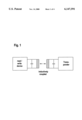
- FIG. 1 is a block diagram of a read/write device and a transponder whose oscillator coils are coupled inductively;
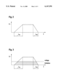
- FIG. 2 is a time chart that illustrates the voltage characteristic of the oscillator coils of the transponder
- FIG. 3 is the same time chart from FIG. 2 but with voltage limiting
- FIG. 4 is a time chart with evaluation of the pulse length
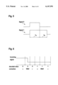
- FIG. 5 is a time chart representing different logical states
- FIG. 6 is a time chart with time windows to evaluate field strength changes.
- FIG. 1 there is shown a block diagram of a read/write device and a transponder with oscillating circuits. These oscillating circuits are harmonized with the carrier frequency of the carrier emitted by the read/write device.
- the oscillator coils are inductively coupled. When the devices are parallel and a short distance from each other, the coupling is very tight. The coupling becomes weaker with distance or when the devices are turned in relation to each other.
- the transponder comprises a voltage limiter, wherein the maximum value of the field strength is no longer always identical with the maximum oscillating circuit voltage.
- the voltage limiter can be simultaneously used to form a switching threshold to recognize field strength changes. It is also possible to operate the voltage limiter only as a protective circuit and additionally provide a voltage comparator that determines a switching threshold to independently recognize field strength changes. This switching threshold must, however, be less than or equal to the value of the voltage limiter.
- FIG. 2 shows a time chart that represents the voltage characteristic of the transponders oscillating circuit coil.
- the read/write device's and transponder's oscillating circuit coil has a oscillating circuit voltage that only gradually rises and falls.
- the rise time from the minimum to the maximum is identified as t an
- the decay time from the maximum to the minimum is identified as t ab .
- the final edge slopes necessarily result from an oscillating circuits limited bandwidth circuit, and depend on its circuit quality.
- FIG. 3 shows the same time chart from FIG. 2 but with voltage limiting.
- a voltage limiter cannot detect the time at which a pulse attains an absolute maximum. Rather it only detects the time at which the field strength change or voltage change reaches or falls below the maximum value set by the voltage limiter. This occurs when it passes through a fixed switching threshold of a voltage comparator.
- different edge slopes of the leading edge and the trailing edge of the pulse arise when the rise time t an and the decay time t ab are largely constant, and that the switching threshold is also constant but that the maximum of the pulse can fluctuate. This leads to different times at which the field strength changes pass through the switching thresholds.
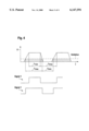
- FIG. 4 shows a time diagram with an evaluation of the pulse length.
- Signal 1 results when the transponder correctly recognizes when the transponder oscillating circuit reaches its maximum field strength or voltage.
- Signal 2 results when the same voltage characteristic at the transponder oscillating circuit is limited.
- Signal 1 can also arise when the voltage is limited when the maximum field strength or voltage coincides with the switching threshold of the voltage limitation.
- Signal 1 and signal 2 contain the same information, but can be interpreted differently.
- the pulse times must therefore be selected to allow sufficient differentiation of different logical states so that possible distortions do not change the information of the transmitted data.
- a pulse with a known duration is sent by the read/write device to the transponder at the beginning of data transmission.
- the transponder measures the pulse length and calibrates the decoder with the measured value. All following pulse times are then evaluated based on this correction value.
- the coupling can fluctuate between the read/write device and the transponder, and the received pulse times can also fluctuate.
- the calibration therefore has to be adjusted. Since the difference between the pulse times of different logical states is constant, the distortions of the pulse times only have an effect on the absolute times and not on their differences.
- FIG. 5 shows two different signals, 0 and 1.
- the signals consist of a constant portion t A , and a portion t B that serves as a differentiating feature between the two signals. Only portion t A is affected by the possible distortions. Therefore only one time must be determined for correction and compensation, and it is subtracted from all the incoming pulse times or added to the incoming pulse times to compensate for the distortions.
- Specific times are expected for the different information (e.g., binary data transmission 0 and 1) after compensation. If the received pulse times no longer correspond to the expected ideal values, the compensation value must be adapted.
- the adaptation can be carried out by forming the difference between the received time and the ideal time or by simply increasing or lowering the compensation value by a step.
- FIG. 6 shows a time diagram with time windows to evaluate field strength changes by classifying an incoming pulse and deriving a correction value.
- the edge of the example pulse falls at an ideal time within range 0.
- the pulse is decoded as 0 or 1 depending on the duration. Limits of a middle time window for ideal field strength changes are formed by permissible tolerances that are symmetrical to the foreseeable time of the field strength change. A slight change in the pulse time therefore does not lead to a misinterpretation. If the pulse time lies outside of the ideal value, the correction value is adapted. In the windows marked with +, the correction value must be changed so that the pulse times to be evaluated are longer, and the opposite is true for the windows marked with -.
- the time range for the ideal pulse width can also be selected as 0 to reduce switching.
Landscapes
- Engineering & Computer Science (AREA)
- Artificial Intelligence (AREA)
- Computer Vision & Pattern Recognition (AREA)
- Physics & Mathematics (AREA)
- General Physics & Mathematics (AREA)
- Theoretical Computer Science (AREA)
- Near-Field Transmission Systems (AREA)
- Radar Systems Or Details Thereof (AREA)
Priority Applications (3)
| Application Number | Priority Date | Filing Date | Title |
|---|---|---|---|
| DE19731035A DE19731035B4 (de) | 1997-07-18 | 1997-07-18 | Verfahren zur Datenübertragung zwischen einem Schreib-Lesegerät und einem Transponder |
| EP98111399A EP0892358A3 (de) | 1997-07-18 | 1998-06-20 | Verfahren zur Datenübertragung zwischen einem Schreib-Lesegerät und einem Transponder |
| US09/174,531 US6147591A (en) | 1997-07-18 | 1998-10-16 | Process for transmitting data between a read/write device and a transponder |
Applications Claiming Priority (2)
| Application Number | Priority Date | Filing Date | Title |
|---|---|---|---|
| DE19731035A DE19731035B4 (de) | 1997-07-18 | 1997-07-18 | Verfahren zur Datenübertragung zwischen einem Schreib-Lesegerät und einem Transponder |
| US09/174,531 US6147591A (en) | 1997-07-18 | 1998-10-16 | Process for transmitting data between a read/write device and a transponder |
Publications (1)
| Publication Number | Publication Date |
|---|---|
| US6147591A true US6147591A (en) | 2000-11-14 |
Family
ID=26038421
Family Applications (1)
| Application Number | Title | Priority Date | Filing Date |
|---|---|---|---|
| US09/174,531 Expired - Fee Related US6147591A (en) | 1997-07-18 | 1998-10-16 | Process for transmitting data between a read/write device and a transponder |
Country Status (3)
| Country | Link |
|---|---|
| US (1) | US6147591A (de) |
| EP (1) | EP0892358A3 (de) |
| DE (1) | DE19731035B4 (de) |
Cited By (8)
| Publication number | Priority date | Publication date | Assignee | Title |
|---|---|---|---|---|
| US20050225447A1 (en) * | 2004-04-13 | 2005-10-13 | Impinj, Inc., A Delaware Corporation | RFID readers transmitting preambles denoting communication parameters and RFID tags interpreting the same and methods |
| US20050237162A1 (en) * | 2004-04-13 | 2005-10-27 | Impinj, Inc., A Delaware Corporation | RFID readers transmitting preambles denoting data rate and methods |
| US20070126584A1 (en) * | 2004-04-13 | 2007-06-07 | Impimj, Inc. | Adaptable Detection Threshold for RFID Tags and Chips |
| US20080031317A1 (en) * | 2006-02-10 | 2008-02-07 | Atmel Germany Gmbh | Method for wireless data transmission between a base station and a transponder via inductive coupling |
| US20090009291A1 (en) * | 2006-11-27 | 2009-01-08 | Martin Berhorst | Method for wireless data transmission between a base station and a passive transponder, as well as a passive transponder |
| US20100182129A1 (en) * | 2005-04-29 | 2010-07-22 | Impinj, Inc. | Interference rejection in rfid tags |
| US7928843B2 (en) | 2001-02-12 | 2011-04-19 | Symbol Technologies, Inc. | Method, system, and apparatus for communications in a RFID system |
| US8763915B2 (en) | 2011-02-01 | 2014-07-01 | Eyes Open Corporation | Identification plate with adjustable damping |
Families Citing this family (7)
| Publication number | Priority date | Publication date | Assignee | Title |
|---|---|---|---|---|
| DE19927318A1 (de) * | 1999-06-15 | 2000-12-21 | Mannesmann Vdo Ag | Verfahren zur drahtlosen Übertragung von Daten |
| US6396438B1 (en) | 1999-09-24 | 2002-05-28 | Slc Technologies | System and method for locating radio frequency identification tags using three-phase antenna |
| US6452504B1 (en) | 1999-09-24 | 2002-09-17 | Ge Interlogix, Inc. | System and method for communication with radio frequency identification tags using tow message DFM protocol |
| US6661335B1 (en) | 1999-09-24 | 2003-12-09 | Ge Interlogix, Inc. | System and method for locating radio frequency identification tags |
| US6693511B1 (en) | 1999-09-24 | 2004-02-17 | Ge Interlogix, Inc. | System and method for communicating with dormant radio frequency identification tags |
| ATE344502T1 (de) * | 2000-03-24 | 2006-11-15 | Infineon Technologies Ag | Dekodiervorrichtung |
| DE10060800A1 (de) * | 2000-12-07 | 2002-06-13 | Tbn Identifikation Und Netzwer | System zur Abfrage von Transpondern und Verfahren zur Ansteuerung eines Gates |
Citations (4)
| Publication number | Priority date | Publication date | Assignee | Title |
|---|---|---|---|---|
| US4206421A (en) * | 1976-09-17 | 1980-06-03 | Siemens Aktiengesellschaft | Arrangement for synchronizing a free-swinging oscillator |
| US5105190A (en) * | 1986-04-22 | 1992-04-14 | N.V. Nederlandsche Apparatenfabriek Nedap | Electromagnetic identification system |
| US5124699A (en) * | 1989-06-30 | 1992-06-23 | N.V. Netherlandsche Apparatenfabriek Nedap | Electromagnetic identification system for identifying a plurality of coded responders simultaneously present in an interrogation field |
| US5491471A (en) * | 1991-10-23 | 1996-02-13 | Stobbe; Anatoli | Access control system where the card controls the transmission format of the card reader |
Family Cites Families (7)
| Publication number | Priority date | Publication date | Assignee | Title |
|---|---|---|---|---|
| DE3447560A1 (de) * | 1984-12-21 | 1986-07-10 | Angewandte Digital Elektronik Gmbh, 2051 Brunstorf | Einrichtung zur beruehrungslosen signal- und energieuebertragung |
| US5091729A (en) * | 1988-12-23 | 1992-02-25 | Hughes Aircraft Company | Adaptive threshold detector |
| DE4003410A1 (de) * | 1990-02-05 | 1991-08-08 | Anatoli Stobbe | Tragbares feldprogrammierbares detektierplaettchen |
| DE4104040C2 (de) * | 1991-02-09 | 2002-08-14 | Thomson Brandt Gmbh | Verfahren zum Abgleich und Betrieb einer Schaltungsanordnung sowie Schaltungsanordnung zur Durchführung des Verfahrens |
| DE69323460T2 (de) * | 1992-09-07 | 1999-07-08 | Denso Corp., Kariya, Aichi | Kommunikationssystem |
| US5450088A (en) * | 1992-11-25 | 1995-09-12 | Texas Instruments Deutschland Gmbh | Transponder arrangement |
| JPH09142257A (ja) * | 1995-11-22 | 1997-06-03 | Tokai Rika Co Ltd | 送受信システム |
-
1997
- 1997-07-18 DE DE19731035A patent/DE19731035B4/de not_active Expired - Fee Related
-
1998
- 1998-06-20 EP EP98111399A patent/EP0892358A3/de not_active Withdrawn
- 1998-10-16 US US09/174,531 patent/US6147591A/en not_active Expired - Fee Related
Patent Citations (4)
| Publication number | Priority date | Publication date | Assignee | Title |
|---|---|---|---|---|
| US4206421A (en) * | 1976-09-17 | 1980-06-03 | Siemens Aktiengesellschaft | Arrangement for synchronizing a free-swinging oscillator |
| US5105190A (en) * | 1986-04-22 | 1992-04-14 | N.V. Nederlandsche Apparatenfabriek Nedap | Electromagnetic identification system |
| US5124699A (en) * | 1989-06-30 | 1992-06-23 | N.V. Netherlandsche Apparatenfabriek Nedap | Electromagnetic identification system for identifying a plurality of coded responders simultaneously present in an interrogation field |
| US5491471A (en) * | 1991-10-23 | 1996-02-13 | Stobbe; Anatoli | Access control system where the card controls the transmission format of the card reader |
Cited By (19)
| Publication number | Priority date | Publication date | Assignee | Title |
|---|---|---|---|---|
| US7928843B2 (en) | 2001-02-12 | 2011-04-19 | Symbol Technologies, Inc. | Method, system, and apparatus for communications in a RFID system |
| US7965189B2 (en) | 2001-02-12 | 2011-06-21 | Symbol Technologies, Inc. | Radio frequency identification architecture |
| US7973643B2 (en) | 2004-04-13 | 2011-07-05 | Impinj, Inc. | RFID readers transmitting preambles denoting data rate and methods |
| US20050237162A1 (en) * | 2004-04-13 | 2005-10-27 | Impinj, Inc., A Delaware Corporation | RFID readers transmitting preambles denoting data rate and methods |
| US20070126584A1 (en) * | 2004-04-13 | 2007-06-07 | Impimj, Inc. | Adaptable Detection Threshold for RFID Tags and Chips |
| US8258955B1 (en) | 2004-04-13 | 2012-09-04 | Impinj, Inc. | Adaptable detection threshold for RFID tags and chips |
| US20050225447A1 (en) * | 2004-04-13 | 2005-10-13 | Impinj, Inc., A Delaware Corporation | RFID readers transmitting preambles denoting communication parameters and RFID tags interpreting the same and methods |
| US7501953B2 (en) * | 2004-04-13 | 2009-03-10 | Impinj Inc | RFID readers transmitting preambles denoting communication parameters and RFID tags interpreting the same and methods |
| US7917088B2 (en) | 2004-04-13 | 2011-03-29 | Impinj, Inc. | Adaptable detection threshold for RFID tags and chips |
| US20100182129A1 (en) * | 2005-04-29 | 2010-07-22 | Impinj, Inc. | Interference rejection in rfid tags |
| US8391785B2 (en) | 2005-04-29 | 2013-03-05 | Impinj, Inc. | Interference rejection in RFID tags |
| US20080031317A1 (en) * | 2006-02-10 | 2008-02-07 | Atmel Germany Gmbh | Method for wireless data transmission between a base station and a transponder via inductive coupling |
| US7953146B2 (en) * | 2006-02-10 | 2011-05-31 | Atmel Corporation | Method for wireless data transmission between a base station and a transponder via inductive coupling |
| US8363737B2 (en) | 2006-02-10 | 2013-01-29 | Atmel Corporation | Wireless data transmission between a base station and a transponder via inductive coupling |
| US20090009291A1 (en) * | 2006-11-27 | 2009-01-08 | Martin Berhorst | Method for wireless data transmission between a base station and a passive transponder, as well as a passive transponder |
| US20120194323A1 (en) * | 2006-11-27 | 2012-08-02 | Martin Berhorst | Method for Wireless Data Transmission Between a Base Station and a Passive Transponder, as Well as a Passive Transponder |
| US8165193B2 (en) * | 2006-11-27 | 2012-04-24 | Atmel Corporation | Method for wireless data transmission between a base station and a passive transponder, as well as a passive transponder |
| US8699560B2 (en) * | 2006-11-27 | 2014-04-15 | Atmel Corporation | Method for wireless data transmission between a base station and a passive transponder, as well as a passive transponder |
| US8763915B2 (en) | 2011-02-01 | 2014-07-01 | Eyes Open Corporation | Identification plate with adjustable damping |
Also Published As
| Publication number | Publication date |
|---|---|
| EP0892358A2 (de) | 1999-01-20 |
| EP0892358A3 (de) | 2000-06-28 |
| DE19731035A1 (de) | 1999-01-28 |
| DE19731035B4 (de) | 2004-09-02 |
Similar Documents
| Publication | Publication Date | Title |
|---|---|---|
| US6147591A (en) | Process for transmitting data between a read/write device and a transponder | |
| EP0242906B1 (de) | Elektromagnetisches Identifizierungssystem | |
| CN100350753C (zh) | 在基站与应答器之间无线数据传输的方法 | |
| US8314685B2 (en) | Data detector for UHF RFID tags | |
| EP0377257A1 (de) | Identifizierungssystem | |
| US6836208B2 (en) | Contactless data transmission system and method for contactless data transmission | |
| US7598872B2 (en) | Method for recognizing identification media | |
| US4495529A (en) | Qualifier circuit | |
| US8727217B2 (en) | Data detector for UHF RFID tags | |
| EP1920381B1 (de) | Verfahren und rfid-lesegerät zur evaluierung eines datenstromsignals in bezug auf daten und / oder kollision | |
| US6633620B2 (en) | Data receiver capable of invalidating erroneous pulses | |
| US5727022A (en) | Method for improving the signal-to-noise ratio in a transmission system by the formation of area equivalents | |
| JP2736830B2 (ja) | データ伝送装置およびこれに用いられる質問装置 | |
| US5969547A (en) | Analog signal processing circuit with noise immunity and reduced delay | |
| US10439659B1 (en) | Device to minimize current overshoot in detuned antenna | |
| JP2001036591A (ja) | データの無線による電磁的伝送方法 | |
| US4653114A (en) | Automatic terminal signal equalization | |
| US7545892B2 (en) | Method and circuit for controlling the input signal for a contactless transponder | |
| GB2623233A (en) | Proximity sensor based communications interface for electronic devices | |
| US6031404A (en) | Analog-signal to square-wave-signal reshaping system with offset compensation | |
| JP4122337B2 (ja) | 非接触トランスポンダの入力信号を調整する方法 | |
| US6751578B2 (en) | Method and apparatus for evaluating a digital information signal | |
| JP2001005922A (ja) | 非接触icカードリーダ装置 | |
| JP3829303B2 (ja) | データの伝送方法 | |
| US20220190792A1 (en) | Wave-shaping for over- and undershoot prevention |
Legal Events
| Date | Code | Title | Description |
|---|---|---|---|
| AS | Assignment |
Owner name: ANATOLI STOBBE, GERMANY Free format text: ASSIGNMENT OF ASSIGNORS INTEREST;ASSIGNOR:SCHEFFLER, HARTMUT;REEL/FRAME:009574/0933 Effective date: 19981015 |
|
| FPAY | Fee payment |
Year of fee payment: 4 |
|
| FPAY | Fee payment |
Year of fee payment: 8 |
|
| REMI | Maintenance fee reminder mailed | ||
| LAPS | Lapse for failure to pay maintenance fees | ||
| LAPS | Lapse for failure to pay maintenance fees |
Free format text: PATENT EXPIRED FOR FAILURE TO PAY MAINTENANCE FEES (ORIGINAL EVENT CODE: EXP.); ENTITY STATUS OF PATENT OWNER: SMALL ENTITY |
|
| STCH | Information on status: patent discontinuation |
Free format text: PATENT EXPIRED DUE TO NONPAYMENT OF MAINTENANCE FEES UNDER 37 CFR 1.362 |
|
| FP | Lapsed due to failure to pay maintenance fee |
Effective date: 20121114 |