US6147633A - Analog-to-digital converter having offset removing function - Google Patents
Analog-to-digital converter having offset removing function Download PDFInfo
- Publication number
- US6147633A US6147633A US09/079,008 US7900898A US6147633A US 6147633 A US6147633 A US 6147633A US 7900898 A US7900898 A US 7900898A US 6147633 A US6147633 A US 6147633A
- Authority
- US
- United States
- Prior art keywords
- filter
- output
- delta
- high pass
- coefficient
- Prior art date
- Legal status (The legal status is an assumption and is not a legal conclusion. Google has not performed a legal analysis and makes no representation as to the accuracy of the status listed.)
- Expired - Lifetime
Links
- 230000008859 change Effects 0.000 claims abstract description 6
- 230000006870 function Effects 0.000 claims description 12
- 238000000034 method Methods 0.000 claims description 6
- 230000009467 reduction Effects 0.000 abstract description 3
- 238000010586 diagram Methods 0.000 description 16
- 238000013459 approach Methods 0.000 description 7
- 230000007704 transition Effects 0.000 description 5
- 238000001914 filtration Methods 0.000 description 3
- 238000006243 chemical reaction Methods 0.000 description 2
- 230000008901 benefit Effects 0.000 description 1
- 230000000295 complement effect Effects 0.000 description 1
- 238000012986 modification Methods 0.000 description 1
- 230000004048 modification Effects 0.000 description 1
- 238000009877 rendering Methods 0.000 description 1
Images



Classifications
-
- H—ELECTRICITY
- H03—ELECTRONIC CIRCUITRY
- H03M—CODING; DECODING; CODE CONVERSION IN GENERAL
- H03M3/00—Conversion of analogue values to or from differential modulation
- H03M3/30—Delta-sigma modulation
- H03M3/322—Continuously compensating for, or preventing, undesired influence of physical parameters
- H03M3/352—Continuously compensating for, or preventing, undesired influence of physical parameters of deviations from the desired transfer characteristic
- H03M3/354—Continuously compensating for, or preventing, undesired influence of physical parameters of deviations from the desired transfer characteristic at one point, i.e. by adjusting a single reference value, e.g. bias or gain error
- H03M3/356—Offset or drift compensation
-
- H—ELECTRICITY
- H03—ELECTRONIC CIRCUITRY
- H03M—CODING; DECODING; CODE CONVERSION IN GENERAL
- H03M3/00—Conversion of analogue values to or from differential modulation
- H03M3/30—Delta-sigma modulation
- H03M3/458—Analogue/digital converters using delta-sigma modulation as an intermediate step
Definitions
- the present invention relates generally to a delta-sigma ( ⁇ ) type analog-to-digital converter, and more particularly to removal of a DC component in a ⁇ type analog-to-digital converter.
- ⁇ delta-sigma
- Prior art approaches for removing a DC component or offset employed in conventional ⁇ type analog-to-digital converters may be roughly classified into two types: an offset calibration method and a method utilizing a high pass filter.
- An example of the offset calibration method is disclosed in U.S. Pat. No. 4,943,807 in which an offset value of a ⁇ A/D converter is stored in a memory, and subtracted from a digitally converted value (a value after passing through a ⁇ modulator and a decimation filter) to remove the DC component.
- the second approach utilizing a high pass filter passes a digitally converted value through a high pass filter to remove a DC component possibly included in the digitally converted value.
- the high pass filter approach In the offset calibration method, if certain external factors or the like cause an offset value to change during a long time operation of an A/D converter, a difference between a value initially stored in a memory and the changed offset value is produced, thereby preventing complete removal of an associated DC component.
- the high pass filter approach is effective to remove an offset varying during operation of an A/D converter as well.
- the high pass filter approach utilizes a filter having an extremely low cut-off frequency which is characteristic required to remove a DC component, it takes a long time to remove the first DC component from the start of operation of the filter. Such a removal time, in fact, occupies a substantial portion within a total time required from power-on of the A/D converter to output of a stable correct value.
- the present invention provides a delta-sigma type digital-to-analog converter for receiving an analog input signal to generate a digital output signal representing the analog input signal in a digital form, comprising: a) a delta-sigma type modulator connected to receive the analog input signal for generating a modulated output; b) a decimation filter connected to receive the modulated output for generating a decimation filter output; c) a high pass filter connected to receive the decimation filter output for generating a high pass filter output, the high pass filter having a variable filter coefficient during operation; and d) filter coefficient control means connected to the high pass filter for generating a coefficient control signal for specifying a change in the variable filter coefficient during operation.
- variable filter coefficients may be changed upon powering up the converter.
- the characteristic of the high pass filter may be represented by using a Z function as follows: ##EQU1## where a l and b l are coefficients, and M and N are positive integers, and the variable filter coefficients may include a first filter coefficient comprising a first combination of values of a l and b l and a second filter coefficient comprising a second combination of values of a 1 and b 1 , where the second combination is different from the first combination.
- the high pass filter is a first-order filter, the characteristic of which is represented by using a Z function as follows: ##EQU2## where k is a coefficient, and the variable filter coefficient may include a first filter coefficient comprising a first value of k and a second filter coefficient comprising a second value of k. In this case, the first filter coefficient has a value close to one; and the second filter coefficient has a value equal or close to zero.
- the high pass filter comprises: a) a subtracter having a first input connected to receive the decimation filter output, a second input, and an output; b) delay means having an input connected to the output of the subtracter and an output; c) an adder having a first input connected to receive the decimation filter output, a second input connected to the output of the delay means, and an output for generating the high pass filter output; and d) a feedback circuit having an input connected to the output of the adder, and an output connected to the second input of the subtracter, the feedback circuit having a variable feedback coefficient during operation, the feedback coefficient acting as the filter coefficients.
- the feedback circuit may be of an adder type or of a multiplier type.
- the filter coefficient control means may include timing control means for supplying a first timing signal as the coefficient control signal; and the first timing signal may indicate that the second filter coefficient is to be used during a first predetermined period of time after the time the converter is reset.
- the delta-sigma type analog-to-digital converter may further comprise dither control means for controlling the application of a DC dither component to the input of the delta-sigma modulator.
- the timing control means may further generate a second timing signal supplied to the dither control means, and the second timing signal may indicate that the DC dither component is not to be applied during a second predetermined period of time after the converter is reset, where the second predetermined period of time is shorter than the first predetermined period of time.
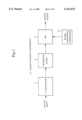
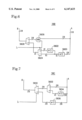
- FIG. 1 is a block diagram illustrating a ⁇ type analog-to-digital converter A according to a first embodiment of the present invention
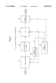
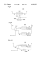
- FIG. 2 is a block diagram illustrating a ⁇ type analog-to-digital converter B according to a second embodiment of the present invention
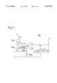
- FIG. 3 is a circuit diagram illustrating in detail a high pass filter shown in FIG. 2;
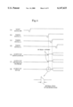
- FIG. 4 is a timing diagram for explaining the operation of the entire ⁇ analog-to-digital converter of FIG. 2 having the high pass filter of FIG. 3;
- FIG. 5 is a circuit diagram illustrating a circuit 38A which is a second embodiment of a feedback circuit 38 within the high pass filter 30 of FIG. 3;
- FIG. 6 is a circuit diagram illustrating a circuit 38B which is a third embodiment of the feedback circuit 38;
- FIG. 7 is a circuit diagram illustrating a circuit 38C which is a fourth embodiment of the feedback circuit 38;
- FIG. 8 is a circuit diagram illustrating a circuit 38D which is a fifth embodiment of the feedback circuit 38;
- FIG. 9 is a circuit diagram illustrating a circuit 38E which is a sixth embodiment of the feedback circuit 38;
- FIG. 10 is a circuit diagram illustrating a circuit 38F which is a seventh embodiment of the feedback circuit 38;
- FIG. 11 is a circuit diagram illustrating a circuit 38G which is an eighth embodiment of the feedback circuit 38;
- FIG. 12 is a circuit diagram illustrating a circuit 38H which is a ninth embodiment of the feedback circuit 38;
- FIG. 13 is a circuit diagram illustrating a circuit 38I which is a tenth embodiment of the feedback circuit 38;
- FIG. 14 is a circuit diagram illustrating a circuit 38J which is an eleventh embodiment of the feedback circuit 38.
- FIG. 15 is a circuit diagram illustrating a circuit 38K which is a twelfth embodiment of the feedback circuit 38.
- FIG. 1 is a block diagram illustrating a first embodiment A of a ⁇ type analog-to-digital (A/D) converter according to the present invention.
- the converter A comprises a ⁇ modulator 1, a decimation filter 2, a high pass filter (HPF) 3, and a filter coefficient controller 4.
- the ⁇ modulator 1 receives an analog input to be converted into a digital form at its input, and generates a modulated output, after being subjected to ⁇ modulation, at its output.
- the modulated output is received by the decimation filter 2 at its input, which decimates the input to generate the result at its output.
- the subsequent HPF 3 has an input, a control input and an output, and also has a group of variable filter coefficients.
- the characteristic of the HPF 3 is generally represented using a Z function as follows: ##EQU3## where a l and b l are coefficients, and M and N are positive integers.
- the variable filter coefficients are constituted by a first group of filter coefficients comprising a first combination of a l and b l values and a second group of filter coefficients comprising a second combination of a l and b l values which are different from those of the first combination.
- the filter coefficients are such that the time constant of the HPF 3 is larger as the cut-off frequency of the HPF 3 approaches to zero.
- the HPF 3 receives the output of the decimation filter 2 at its input, a signal for controlling the filter coefficient at its control input, and generates the result of high pass filtering performed on the received decimation filter output with specified filter coefficients.
- the filter coefficient controller 4 has its output connected to the control input of the HPF 3, so that the filter coefficient controller 4 supplies the HPF 3 with the filter coefficient control signal to cause the HPF 3 to use appropriate values as the HPF coefficients.
- the configuration described above enables the HPF 3 to execute the filtering using a group of filter coefficients specified by the controller 4 during an A/D converting operation of the A/D converter A, thereby making it possible to execute the high pass filtering with an appropriate time constant or a cut-off frequency in accordance with a particular operating situation.
- a large value may be used as the filter time constant when an offset of the A/D converter is to be removed, while a smaller value may be used as the time constant of the HPF 3 when a digital output is to be stabilized as soon as possible, for example, when the A/D converter A is powered on.
- the converter B which comprises the converter A shown in FIG. 1 with a portion thereof being more specific, includes a ⁇ modulator 10, a decimation filter 20 and a HPF 30, similar to the components 1, 2 and 3 in FIG. 1 respectively. Also, the converter B includes a timing controller 40 partially corresponding to the filter coefficient controller 4 (FIG. 1), a serial controller 50 and a dither controller 60.
- the HPF 30 comprises a first-order filter, the characteristic of which can be represented using a Z function as follows: ##EQU4## where k is a coefficient. The coefficient k is a variable coefficient as mentioned above.
- a first filter coefficient equal to a first value of k and a second filter coefficient equal to a second value of k are used.
- the filter coefficient k may take a value, for example, in the range of zero to one.
- the time constant of the HPF 30 becomes larger, with the cut-off frequency of the HPF 30 being closer to zero.
- the filter coefficient approaches zero the time constant of the HPF 30 becomes smaller, with the cut-off frequency of the HPF 30 becoming higher.
- the serial controller 50 converts a parallel filter output from the HPF 30 into a serial form.
- the dither controller 60 controls the application of a DC bias voltage (a bias voltage source (not shown) is provided within the ⁇ modulator 10) of a certain magnitude to an analog input received at an input of the ⁇ modulator 10, so that the tone frequency is moved out of an audio frequency band.
- the ⁇ modulator 10 also has first and second control inputs which are connected to receive a signal from the timing controller 40 and a control input from the dither controller 60, respectively.
- the first control input opens or closes an input gate (not shown) which is provided to receive an analog input to the modulator 10.
- the second control input opens or closes an input gate (not shown) which is provided to pass a dither to an adder (not shown) for the addition of the dither to the received analog input.
- the serial controller 50 also has a control input which activates its serial digital output depending upon the logical state of the control input.
- the timing controller 40 generates several timing signals to control the operation of the converter B.
- a first timing signal I1 is supplied to the control input of the HPF 30 and to the first control input of the modulator 10.
- a second timing signal I2 is supplied to the input of the dither controller 60, while a third timing signal I3 is supplied to the control input of the serial controller 50.
- the HPF 30 comprises a subtracter 32, a one-clock delay 34, an adder 36, and a feedback circuit 38.
- the converter B is operated with a clock having a frequency of 44.1 KHz.
- the subtracter 32 receives at its negative input a 28-bit binary input X which is the output of the decimation filter 20 (see FIG. 2).
- the subtracter 32 subtracts the input X from a value received at its positive input to generate the subtraction result as a 28-bit binary output.
- the output of the subtracter 32 is supplied to one of positive inputs of an adder 36 which also receives the input X at the other positive input.
- the adder 36 adds both the inputs to generate the addition result as a 28-bit binary output Y.
- the output Y is supplied to the input of the subsequent serial controller 50 (see FIG. 2).
- the output Y is also supplied as an input A of the feedback circuit 38 which generates a binary feedback output B applied to the positive input of the subtracter 32.
- the feedback circuit 38 is an adder type in which two non-zero filter coefficients (or feedback coefficients) k1 and k2 are selectively used.
- the filter coefficient k1 is "8191/8192" and therefore approximately equals to one, while the filter coefficient k2 is "1/8192" and therefore is approximately equal to zero.
- the feedback circuit 38 comprises an adder 3800, a shift circuit 3802 for shifting an input to the left by 13 bits (represented by " ⁇ 13"), 41 (indicated by "X41") AND gates 3804, 28 (indicated by "X28”) exclusive OR (EX-OR) gates 3806, and an inverter 3808.
- the adder 3800 internally generates a 41-bit binary signal C[40:0] from a 28-bit input A [27:0] received at its negative input by extending the most significant bit (MSB) of the input A [27:0].
- MSB most significant bit
- the input A is multiplied by one while extending its bit length to 41 bits (it should be noted that binary signals are represented by a two's compliment).
- each bit in a portion [40:28] of the extended binary signal C [40:0] is equal to the bit A[27], while bits C[27:0] are equal to the corresponding bits A[27:0], respectively.
- bits D[40:13] equals to bits A [27:0].
- Bits D[12:0] are all equal to zero.
- the adder 3800 subtracts the binary signal C[40:0] from the binary signal E[40:0] to generate only the upper 28 bits of the subtraction result as F[27:0]. Since the lower 13 bits are not used, this is equivalent to a multiplication by 2 -13 .
- the signal F at this time is equal to (E-C)/8192.
- a reset signal RS (not shown in FIG. 2) which is applied to the timing controller 40 from a system using the A/D converter of the invention, transitions from low to high at time t1 due to the A/D converter being powered on.
- the timing controller 40 Based on the high reset signal RS, the timing controller 40 forms and generates the timing signals I1, I2 and I3 as shown in (c), (b) and (d) of FIG. 4, respectively.
- the timing signals I1, I2 and I3 are initially at low.
- the input gate of the modulator 10 for receiving an analog input is closed, and the input gate within the modulator 10 for the application of a DC dither is also closed.
- the HPF 30 takes the filter coefficient k2 (substantially zero).
- a digital output of the serial controller 50 is not yet activated. With this condition, the timing signal I2 first transitions from low to high at time t2, for example, 300 milliseconds after time t1, whereby the dither controller 60 causes a DC bias to be added to the analog input within the modulator 10.
- the timing signal I1 transitions to high. This opens the input gate of the ⁇ modulator 10 to start A/D conversion of an analog input, while at the same time the filter coefficient of the HPF 30 is switched from k1 to k2 (substantially one). As a result, the offset removing function in the A/D conversion is fully activated.
- the timing signal I3 transitions from low to high, causing the digital output of the serial controller 50 to be active, whereby the A/D converted output is generated in a serial form.
- the A/D converter according to one embodiment of the present invention has been described above.
- the feedback circuit portion of the HPF 30 can be implemented by a variety of circuit configurations, some of which will be described for the purpose of illustration.
- FIG. 5 illustrates a circuit 38A according to a second embodiment of the feedback circuit 38 of the HPF 30.
- the embodiment shown in FIG. 5 is intended to provide a circuit free from a one-bit error which can occur in the circuit of FIG. 3.
- the feedback circuit 38A of FIG. 5 includes an AND gate 3810 and an adder 3812 in addition to the circuit 38 of FIG. 3.
- the AND gate 3810 receives the output of the inverter 3808 at one of the inputs and a binary "1" signal at the other input.
- the output of the AND gate 3810 is received by one of the inputs of the adder 3812 which also receives the output G[27:0] from the EX-OR gates 3806 at the other input.
- FIG. 6 illustrates a feedback circuit 38B according to a third embodiment of adder type which is free from the bit error and has two coefficients k1 and k2 having the same values as the aforementioned non-zero values, i.e., "8191/8192" and "1/8192".
- the coefficients are realized in the following manner.
- a 13-bit left shift circuit 3820 multiplies an input A by 8192.
- the output of the shift circuit 3820 is applied to a shift circuit 3822 which shifts the output to the right by 13 bits (represented by "22 >13"), that is, divides the output by 8192, such that the output of the shift circuit 3822 is equal to the input A multiplied by one.
- a selector 3824 at the next stage receives the output of the shift circuit 3820 at a "1" input, the output of the shift circuit 3822 at a "0" input, and the timing signal I1 at a selection control input.
- An output of the selector 3824 is connected to a positive input of an adder 3826 which has a negative input connected to outputs of a set of 28 AND gates 3828.
- Each of the AND gates 3828 receives a corresponding bit of the input A at one of the inputs and the timing signal I1 at the other input.
- the adder 3826 is similar to the adder 3800 in FIG. 3.
- the adder 3826 performs bit extension at its negative input, and provides an output formed only by the most significant 28 bits of the 41 bits such that the adder 3826 has a function of performing a multiplication by 1/8192.
- FIG. 7 illustrates a feedback circuit 38C according to a fourth embodiment for use in the HPF 30, which is also an adder type one free from bit error and having non-zero coefficients.
- the feedback circuit 38C realizes a coefficient k1 using a signal at a "1" input terminal of a selector 3830 and a coefficient k2 using a signal at a "0" input terminal of the selector 3830.
- an adder 3832 which is similar to the adder 3800 in FIG. 3, has a negative input connected to receive an input A multiplied by one and a positive input connected to receive 8192 ⁇ A generated by a 13-bit left shift circuit 3834 placed at the preceding stage.
- the "0" input terminal of the selector 3830 receives (1/8192) ⁇ A generated by a 13-bit right shift circuit 3836.
- a feedback circuit 38D comprises a multiplier 3840, a k1 coefficient circuit 3842, a k2 coefficient circuit 3844 and a switch 3846.
- the multiplier 3840 receives a signal A at its input and generates a signal B at its output.
- the multiplier 3840 has a coefficient input connected to receive the output of the switch 3846.
- a "1" input terminal of the switch 3846 is connected to receive a coefficient k1 in the form of 13-bit binary signal from the k1 coefficient circuit 3842, while a "0" input terminal of the switch 3846 is connected to receive a coefficient k2 in the form of 13-bit binary signal from the k2 coefficient circuit 3844.
- the control input of the switch 3846 receives a timing signal I1 such that depending upon the status of the timing signal I1, a corresponding one of the input terminals is connected to the output terminal.
- a feedback circuit 38E is the same as the feedback circuit 38D of FIG. 8 except that two multipliers are provided with a coefficient circuit being associated with each multiplier, and that a selector 3847 is provided for selectively generating the outputs of the two multipliers.
- the feedback circuit 38E also functions similar to the feedback circuit 38D, and can advantageously set the coefficient values as desired.
- a feedback circuit 38F is the same as the feedback circuit 38E of FIG. 9 except that a combination of the multiplier and the k2 coefficient circuit is replaced with a ">>13" shift circuit 3848.
- a coefficient k2 is a fixed value of 1/8192.
- Another coefficient k1 can be set as desired.
- a feedback circuit 38G according to an eighth embodiment shown in FIG. 11 comprises an adder 3850 similar to the adder 3800 in FIG. 3, a " ⁇ 13" shift circuit 3852 and a set of 28 AND gates 3854. More specifically, each of the AND gates 3854 receives a corresponding bit of a binary signal A at one of the inputs and a timing signal I1 at the other input. An output from the AND gates 3854 is connected to a negative input of the adder 3850 which has its positive input connected to receive the output from the AND gates 3854 through the left shift circuit 3852.
- a feedback circuit 38H according to a ninth embodiment shown in FIG. 12 is similar to the feedback circuit 38G of FIG. 11 except that AND gates are positioned on the output side of the adder rather than on the input side of the same. More specifically, each of AND gates 3856 has one of the inputs connected to a corresponding one of the 28 bits of the output of the adder 3850, the other input connected to a timing signal I1. The negative input of the adder 3850 and the input of the shift circuit 3852 are connected to receive a signal A.
- the feedback circuit 38H functions in the same manner as the feedback circuit 38G.
- a feedback circuit 38I according to a tenth embodiment comprises a multiplier 3860 which receives a signal A at an input, a k1 coefficient circuit 3862 having an output connected to a coefficient input of the multiplier 3860, and a set of 28 AND gates 3864.
- Each of the AND gates 3864 has one input connected to receive a corresponding one of the 28 bits of an output of the multiplier 3860 and the other input connected to receive a timing signal I1.
- a feedback circuit 38J according to an eleventh embodiment shown in FIG. 14 is similar to the feedback circuit 38I except that a set of 28 AND gates 3866 are not connected to the output side of a multiplier but to the coefficient input of the multiplier.
- the feedback circuit 38J has the same function as the feedback circuit 38I.
- a feedback circuit 38K according to a twelfth embodiment shown in FIG. 15 is also identical to the feedback circuit 38I of FIG. 13 except that a set of 28 AND gates 3868 are positioned on the input side of a multiplier.
- the feedback circuit for use in the HPF 30 can be implemented in a variety of ways, and thus an appropriate one can be employed in accordance with particular use, application, and so on.
- the removal of varying offset and a reduction in time required to generate a stable output of an A/D converter can be realized only by switching filter coefficients of a high pass filter.
- the present invention advantageously reduces a time required to test A/D converters. Further, even when the A/D converter is used in an apparatus having a power down mode for saving power dissipation, the present invention is effective in reducing a time required to generate a stable output every time the apparatus is powered up for recovering from the power down mode.
Landscapes
- Engineering & Computer Science (AREA)
- Theoretical Computer Science (AREA)
- Analogue/Digital Conversion (AREA)
- Compression, Expansion, Code Conversion, And Decoders (AREA)
Applications Claiming Priority (2)
| Application Number | Priority Date | Filing Date | Title |
|---|---|---|---|
| JP9125774A JPH10322214A (ja) | 1997-05-15 | 1997-05-15 | オフセット除去機能付のアナログ−デジタル変換器 |
| JP9-125774 | 1997-05-15 |
Publications (1)
| Publication Number | Publication Date |
|---|---|
| US6147633A true US6147633A (en) | 2000-11-14 |
Family
ID=14918512
Family Applications (1)
| Application Number | Title | Priority Date | Filing Date |
|---|---|---|---|
| US09/079,008 Expired - Lifetime US6147633A (en) | 1997-05-15 | 1998-05-14 | Analog-to-digital converter having offset removing function |
Country Status (2)
| Country | Link |
|---|---|
| US (1) | US6147633A (ja) |
| JP (1) | JPH10322214A (ja) |
Cited By (14)
| Publication number | Priority date | Publication date | Assignee | Title |
|---|---|---|---|---|
| US6661362B2 (en) * | 2000-09-11 | 2003-12-09 | Broadcom Corporation | Methods and systems for high speed quantizers |
| US6839010B1 (en) * | 2002-12-27 | 2005-01-04 | Zilog, Inc. | Sigma-delta analog-to-digital converter with reduced quantization noise |
| US20050030212A1 (en) * | 2000-09-11 | 2005-02-10 | Brooks Todd Lee | Methods and systems for high speed quantizers |
| US6980145B1 (en) * | 2004-07-30 | 2005-12-27 | Broadcom Corporation | System and method for noise cancellation in a signal processing circuit |
| US20060261989A1 (en) * | 2005-05-19 | 2006-11-23 | Neaz Farooqi | Low power sigma delta modulator |
| US7652723B1 (en) | 2004-04-19 | 2010-01-26 | Video Accessory Corporation | Composite video signal correction unit for video imaging and video recording systems |
| US20120025847A1 (en) * | 2009-01-28 | 2012-02-02 | St-Ericsson Sa | Method and sytem for measuring a time constant of an integrated circuit, and integrated circuit provided with such a system |
| US20120043974A1 (en) * | 2010-08-17 | 2012-02-23 | Nxp B.V. | Circuit and method for monitoring a capacitive signal source |
| US8912941B2 (en) | 2012-03-14 | 2014-12-16 | Panasonic Corporation | Analog-digital conversion circuit and method for driving the same |
| US10797715B2 (en) | 2018-11-19 | 2020-10-06 | Infineon Technologies Ag | Filtering method and filter |
| CN112769413A (zh) * | 2019-11-04 | 2021-05-07 | 炬芯科技股份有限公司 | 高通滤波器及其稳定方法以及adc录音系统 |
| CN114070310A (zh) * | 2020-07-30 | 2022-02-18 | 炬芯科技股份有限公司 | 高通滤波方法、高通滤波器和主动降噪系统 |
| US20220206036A1 (en) * | 2020-12-28 | 2022-06-30 | Seiko Epson Corporation | Vibration Rectification Error Correction Device, Sensor Module, And Vibration Rectification Error Correction Method |
| US20230102232A1 (en) * | 2021-09-30 | 2023-03-30 | Nxp B.V. | System and method of replicating and cancelling chopping folding error in delta-sigma modulators |
Families Citing this family (4)
| Publication number | Priority date | Publication date | Assignee | Title |
|---|---|---|---|---|
| JP2002247683A (ja) * | 2001-02-02 | 2002-08-30 | Techtronic As | 内部a/d変換器を備えたマイクロホン |
| US20020106091A1 (en) | 2001-02-02 | 2002-08-08 | Furst Claus Erdmann | Microphone unit with internal A/D converter |
| JP4636926B2 (ja) * | 2005-04-22 | 2011-02-23 | 三洋電機株式会社 | マルチビットδς変調型daコンバータ |
| JP7293744B2 (ja) * | 2019-03-14 | 2023-06-20 | 富士電機株式会社 | 電力変換装置 |
Citations (4)
| Publication number | Priority date | Publication date | Assignee | Title |
|---|---|---|---|---|
| US4943807A (en) * | 1988-04-13 | 1990-07-24 | Crystal Semiconductor | Digitally calibrated delta-sigma analog-to-digital converter |
| US5018429A (en) * | 1988-04-07 | 1991-05-28 | Casio Computer Co., Ltd. | Waveform generating apparatus for an electronic musical instrument using filtered components of a waveform |
| US5144308A (en) * | 1991-05-21 | 1992-09-01 | At&T Bell Laboratories | Idle channel tone and periodic noise suppression for sigma-delta modulators using high-level dither |
| US5327137A (en) * | 1992-04-15 | 1994-07-05 | Joachim Scheerer | Multiple ramp procedure with higher order noise shaping |
-
1997
- 1997-05-15 JP JP9125774A patent/JPH10322214A/ja active Pending
-
1998
- 1998-05-14 US US09/079,008 patent/US6147633A/en not_active Expired - Lifetime
Patent Citations (4)
| Publication number | Priority date | Publication date | Assignee | Title |
|---|---|---|---|---|
| US5018429A (en) * | 1988-04-07 | 1991-05-28 | Casio Computer Co., Ltd. | Waveform generating apparatus for an electronic musical instrument using filtered components of a waveform |
| US4943807A (en) * | 1988-04-13 | 1990-07-24 | Crystal Semiconductor | Digitally calibrated delta-sigma analog-to-digital converter |
| US5144308A (en) * | 1991-05-21 | 1992-09-01 | At&T Bell Laboratories | Idle channel tone and periodic noise suppression for sigma-delta modulators using high-level dither |
| US5327137A (en) * | 1992-04-15 | 1994-07-05 | Joachim Scheerer | Multiple ramp procedure with higher order noise shaping |
Non-Patent Citations (18)
| Title |
|---|
| AD1877 Single Supply 16 Bit Stereo ADC, Analog Devices, pp. 1 17. * |
| AD1877 Single Supply 16-Bit Σ.increment. Stereo ADC, Analog Devices, pp. 1-17. |
| AK4510 Offset Calibration, Asahi Kasei, 1994/5, pp. 1 11. * |
| AK4510 Offset Calibration, Asahi Kasei, 1994/5, pp. 1-11. |
| AK4520 20 Bit Stereo .increment.Σ ADC & DAC, Asahi Kasei, Rev 2.0, 1996/9, pp. 1-20. |
| AK4520 20 Bit Stereo ADC & DAC, Asahi Kasei, Rev 2.0, 1996/9, pp. 1 20. * |
| AK5340 Offset Calibration, Asahi Kasei, 1995/02, pp. 1 18. * |
| AK5340 Offset Calibration, Asahi Kasei, 1995/02, pp. 1-18. |
| AK5350 Enhanced Dual Bit .increment.Σ 20 Bit A/D Converter, Asahi Kasei, 1996/01, pp. 1-15. |
| AK5350 Enhanced Dual Bit 20 Bit A/D Converter, Asahi Kasei, 1996/01, pp. 1 15. * |
| AK5391 Enhanced Dual Bit .increment.Σ 24 Bit ADC, Asahi Kasei, Rev. 1.0, 1995/02, pp. 1-14. |
| AK5391 Enhanced Dual Bit 24 Bit ADC, Asahi Kasei, Rev. 1.0, 1995/02, pp. 1 14. * |
| CS5330/CS5331 8 Pin, Stereo A/D Converter for Digital Audio, Crystal Semiconductor Corporation, Jan. 1995, pp. 1 14. * |
| CS5330/CS5331 8-Pin, Stereo A/D Converter for Digital Audio, Crystal Semiconductor Corporation, Jan. 1995, pp. 1-14. |
| TDA1309H Low Voltage Low Power Stereo Bitstream ADC/DAC, Philips Semiconductors, Jun. 3. 1996, pg. 2 and 3. * |
| TDA1309H Low-Voltage Low-Power Stereo Bitstream ADC/DAC, Philips Semiconductors, Jun. 3. 1996, pg. 2 and 3. |
| TLC320AD57C Sigma Delta Stereo Analog to Digital Converter, Texas Instruments, 1995, 16 pages. * |
| TLC320AD57C Sigma-Delta Stereo Analog-to-Digital Converter, Texas Instruments, 1995, 16 pages. |
Cited By (25)
| Publication number | Priority date | Publication date | Assignee | Title |
|---|---|---|---|---|
| US6661362B2 (en) * | 2000-09-11 | 2003-12-09 | Broadcom Corporation | Methods and systems for high speed quantizers |
| US20050030212A1 (en) * | 2000-09-11 | 2005-02-10 | Brooks Todd Lee | Methods and systems for high speed quantizers |
| US6919832B2 (en) | 2000-09-11 | 2005-07-19 | Broadcom Corporation | Methods and systems for high speed quantizers |
| US7212142B2 (en) | 2000-09-11 | 2007-05-01 | Broadcom Corporation | Methods and systems for high speed quantizers |
| US6839010B1 (en) * | 2002-12-27 | 2005-01-04 | Zilog, Inc. | Sigma-delta analog-to-digital converter with reduced quantization noise |
| US7068197B1 (en) * | 2002-12-27 | 2006-06-27 | Zilog, Inc. | ADC with reduced quantization noise and programmable bit resolution |
| US7652723B1 (en) | 2004-04-19 | 2010-01-26 | Video Accessory Corporation | Composite video signal correction unit for video imaging and video recording systems |
| US6980145B1 (en) * | 2004-07-30 | 2005-12-27 | Broadcom Corporation | System and method for noise cancellation in a signal processing circuit |
| US20060261989A1 (en) * | 2005-05-19 | 2006-11-23 | Neaz Farooqi | Low power sigma delta modulator |
| US7142144B1 (en) * | 2005-05-19 | 2006-11-28 | Ami Semiconductor, Inc. | Low power sigma delta modulator |
| US20070252736A1 (en) * | 2005-05-19 | 2007-11-01 | Neaz Farooqi | Low power sigma delta modulator |
| US7692568B2 (en) | 2005-05-19 | 2010-04-06 | Ami Semiconductor, Inc. | Low power sigma delta modulator with successive approximation converter |
| US20120025847A1 (en) * | 2009-01-28 | 2012-02-02 | St-Ericsson Sa | Method and sytem for measuring a time constant of an integrated circuit, and integrated circuit provided with such a system |
| US9030213B2 (en) * | 2009-01-28 | 2015-05-12 | St-Ericsson Sa | Method and system for measuring a time constant of an integrated circuit, and integrated circuit provided with such a system |
| US20120043974A1 (en) * | 2010-08-17 | 2012-02-23 | Nxp B.V. | Circuit and method for monitoring a capacitive signal source |
| US8912941B2 (en) | 2012-03-14 | 2014-12-16 | Panasonic Corporation | Analog-digital conversion circuit and method for driving the same |
| US10797715B2 (en) | 2018-11-19 | 2020-10-06 | Infineon Technologies Ag | Filtering method and filter |
| CN112769413A (zh) * | 2019-11-04 | 2021-05-07 | 炬芯科技股份有限公司 | 高通滤波器及其稳定方法以及adc录音系统 |
| CN112769413B (zh) * | 2019-11-04 | 2024-02-09 | 炬芯科技股份有限公司 | 高通滤波器及其稳定方法以及adc录音系统 |
| CN114070310A (zh) * | 2020-07-30 | 2022-02-18 | 炬芯科技股份有限公司 | 高通滤波方法、高通滤波器和主动降噪系统 |
| US20220206036A1 (en) * | 2020-12-28 | 2022-06-30 | Seiko Epson Corporation | Vibration Rectification Error Correction Device, Sensor Module, And Vibration Rectification Error Correction Method |
| US11988685B2 (en) * | 2020-12-28 | 2024-05-21 | Seiko Epson Corporation | Vibration rectification error correction device, sensor module, and vibration rectification error correction method |
| US12276673B2 (en) | 2020-12-28 | 2025-04-15 | Seiko Epson Corporation | Vibration rectification error correction device, sensor module, and vibration rectification error correction method |
| US20230102232A1 (en) * | 2021-09-30 | 2023-03-30 | Nxp B.V. | System and method of replicating and cancelling chopping folding error in delta-sigma modulators |
| US11658677B2 (en) * | 2021-09-30 | 2023-05-23 | Nxp B.V. | System and method of replicating and cancelling chopping folding error in delta-sigma modulators |
Also Published As
| Publication number | Publication date |
|---|---|
| JPH10322214A (ja) | 1998-12-04 |
Similar Documents
| Publication | Publication Date | Title |
|---|---|---|
| US6147633A (en) | Analog-to-digital converter having offset removing function | |
| US7429940B2 (en) | Delta-sigma modulator circuit with limiter and method therefor | |
| JPH09121161A (ja) | ディザを利用してシグマ・デルタ変調器の安定性を改善する方法 | |
| US7200187B2 (en) | Modulator for digital amplifier | |
| US20060072657A1 (en) | Pulse width-modulated noise shaper | |
| EP0494738B1 (en) | A sigma-delta modulator for a D/A converter with dither signal | |
| JPH10322214A5 (ja) | ||
| JP4514881B2 (ja) | データ変換器におけるノイズ減衰回路および方法 | |
| EP1665542A1 (en) | A/d converter | |
| EP3776866B1 (en) | Delta sigma modulator systems and methods | |
| US7071860B2 (en) | System and method for noise cancellation in a signal processing circuit | |
| US6147634A (en) | Method and apparatus for digital to analog conversion with reduced noise | |
| JP3303585B2 (ja) | 分散フィードバック式δς変調器 | |
| US6943716B2 (en) | Variable rate sigma delta modulator | |
| WO1999049578A1 (en) | Tone modulation in delta-sigma dac using square wave dither | |
| EP1130786B1 (en) | A digital signal processing device and a method and a delta-sigma modulator using the same method | |
| JP4021333B2 (ja) | デジタル・スイッチング増幅装置 | |
| JPH08139607A (ja) | デルタシグマ変調器のalc回路 | |
| JPH07297646A (ja) | デジタル/アナログ変換回路 | |
| JP2003079134A (ja) | スイッチング電源 | |
| JPH0870251A (ja) | デルタシグマ型ad変換回路 | |
| JP3917190B2 (ja) | 同期シグマ―デルタ変調器 | |
| JP3358728B2 (ja) | Δς変調器 | |
| JP2006503472A (ja) | データコンバータ | |
| JP4361418B2 (ja) | デジタル/アナログ変換回路 |
Legal Events
| Date | Code | Title | Description |
|---|---|---|---|
| AS | Assignment |
Owner name: BURR-BROWN CORPORATION, ARIZONA Free format text: ASSIGNMENT OF ASSIGNORS INTEREST;ASSIGNORS:UKAWA, MASAYUKI;KANAYAMA, HIDEKI;REEL/FRAME:009318/0063 Effective date: 19980622 |
|
| STCF | Information on status: patent grant |
Free format text: PATENTED CASE |
|
| FPAY | Fee payment |
Year of fee payment: 4 |
|
| FPAY | Fee payment |
Year of fee payment: 8 |
|
| FPAY | Fee payment |
Year of fee payment: 12 |
|
| AS | Assignment |
Owner name: TEXAS INSTRUMENTS INCORPORATED, TEXAS Free format text: ASSIGNMENT OF ASSIGNORS INTEREST;ASSIGNOR:TEXAS INSTRUMENTS TUCSON CORPORATION;REEL/FRAME:055382/0476 Effective date: 20210216 |