US6504896B2 - X-ray illumination optical system and x-ray reduction exposure apparatus - Google Patents
X-ray illumination optical system and x-ray reduction exposure apparatus Download PDFInfo
- Publication number
- US6504896B2 US6504896B2 US08/917,373 US91737397A US6504896B2 US 6504896 B2 US6504896 B2 US 6504896B2 US 91737397 A US91737397 A US 91737397A US 6504896 B2 US6504896 B2 US 6504896B2
- Authority
- US
- United States
- Prior art keywords
- reflection type
- ray
- ray beam
- mask
- integrator
- Prior art date
- Legal status (The legal status is an assumption and is not a legal conclusion. Google has not performed a legal analysis and makes no representation as to the accuracy of the status listed.)
- Expired - Fee Related
Links
Images



Classifications
-
- G—PHYSICS
- G03—PHOTOGRAPHY; CINEMATOGRAPHY; ANALOGOUS TECHNIQUES USING WAVES OTHER THAN OPTICAL WAVES; ELECTROGRAPHY; HOLOGRAPHY
- G03F—PHOTOMECHANICAL PRODUCTION OF TEXTURED OR PATTERNED SURFACES, e.g. FOR PRINTING, FOR PROCESSING OF SEMICONDUCTOR DEVICES; MATERIALS THEREFOR; ORIGINALS THEREFOR; APPARATUS SPECIALLY ADAPTED THEREFOR
- G03F7/00—Photomechanical, e.g. photolithographic, production of textured or patterned surfaces, e.g. printing surfaces; Materials therefor, e.g. comprising photoresists; Apparatus specially adapted therefor
- G03F7/70—Microphotolithographic exposure; Apparatus therefor
- G03F7/70058—Mask illumination systems
-
- G—PHYSICS
- G21—NUCLEAR PHYSICS; NUCLEAR ENGINEERING
- G21K—HANDLING OF PARTICLES OR IONISING RADIATION NOT OTHERWISE PROVIDED FOR; IRRADIATION DEVICES; GAMMA RAY OR X-RAY MICROSCOPES
- G21K1/00—Arrangements for handling particles or ionising radiation, e.g. focusing or moderating
- G21K1/06—Arrangements for handling particles or ionising radiation, e.g. focusing or moderating using diffraction, refraction or reflection, e.g. monochromators
Definitions
- This invention relates to an X-ray illumination optical system and an X-ray reduction exposure apparatus using the same and, in another aspect, it relates to a device manufacturing method using such an X-ray reduction exposure apparatus.
- An X-ray reduction projection exposure process is used for the manufacture of microdevices such as semiconductor circuit devices, having fine patterns.
- a mask having a circuit pattern formed thereon is illuminated with X-rays and an image of the pattern of the mask is projected, in a reduced scale, on the surface of a wafer.
- a resist on the wafer surface is sensitized, whereby the pattern is transferred and printed thereon.
- FIG. 12 is a schematic view of a known example of an X-ray reduction projection exposure apparatus
- FIG. 13 is a schematic and perspective view of a reflection type integrator
- FIG. 14 is a schematic view for explaining an illumination region upon the surface of a mask.
- denoted at 1001 is a light emission point for X-rays
- denoted at 1002 is an X-ray beam
- Denoted at 1004 is a first rotational parabolic surface mirror
- denoted at 1005 is a reflection type integrator
- Denoted at 1006 is a second rotational parabolic surface mirror
- denoled at 1007 is a mask.
- Denoted at 1008 is a projection optical system
- denoted at 1009 is a wafer.
- Denoted at 1010 is a mask stage, and denoted at 1011 is a wafer stage.
- Denoted at 1012 is an arcuate aperture, and denoted at 1013 is a laser light source.
- Denoted at 1014 is a laser collecting optical system, and denoted at 1015 is an illumination region defined on the surface of the mask.
- Denoted at 1016 is an arcuate region within which the exposure is performed.
- An X-ray light source may comprise a laser plasma or an undulator.
- X-rays from the light source are collected by means of the first rotational parabolic surface mirror 1004 , and the collected X-ray beam is projected on the reflection type integrator 1005 , whereby secondary light sources are formed.
- X-rays from these secondary light sources are collected by means of the second rotational parabolic surface mirror 1006 , to illuminate the mask 1007 .
- the mask 1007 comprises a multilayered film reflection mirror on which non-reflective portions are defined by use of an X-ray absorptive material, for example, whereby a transfer pattern is formed thereon.
- X-rays reflected by the mask 1007 are imaged by the projection optical system 1008 upon the surface of the wafer 1009 .
- the projection optical system 1008 is designed so as to provide good imaging performance with respect to a narrow arcuate region off the optical axis. In order that the exposure is performed only by use of this narrow arcuate region, an aperture 1012 having an arcuate opening is disposed just before the wafer 1009 .
- the exposure process is performed while scanningly moving the mask 1007 and the wafer 1009 simultaneously.
- the reflection type integrator 1005 may comprise a fly's-eye mirror having a number of small spherical surfaces arrayed two-dimensionally, as is best seen in FIG. 13, which are adapted to define a number of secondary light sources.
- the spatial extension of the secondary light source group is d
- the angular extension of X-rays emitted from each secondary light source is ⁇
- the focal length of the second parabolic surface mirror 1006 is f
- the size of the illumination region 1015 on the mask 1007 surface is f ⁇
- the angular extension of X-rays illuminating a single point on the mask is d/f.
- the coherence factor ⁇ As a parameter which represents the characteristic of the illumination optical system, there is a coherence factor ⁇ . If the mask-side numerical aperture of the projection optical system 1008 is NAp 1 , and the mask-side numerical aperture of the illumination optical system is NAi, the coherence factor can be defined as follows:
- the optimum value of ⁇ is determined by the required resolution and contrast. Generally, if the factor ⁇ is too small, an interference pattern appears at the edge portion of an image of a fine pattern as projected on the wafer 1009 . If the factor ⁇ is too large, the contrast of the projected image reduces.
- ⁇ is zero, it is called coherent illumination.
- a constant value will be shown up to a particular spatial frequency as can be given by NAp 2 / ⁇ where NAp 2 is the wafer-side numerical aperture of the projection optical system and ⁇ is the wavelength of the X-ray beam. For a higher frequency above the particular frequency, it becomes equal to zero, and resolving is not attainable.
- ⁇ is equal to 1, it is called incoherent illumination.
- the transfer function OTF reduces with an increase in the spatial frequency, but it does not become equal to zero unless a particular spatial frequency given by 2 ⁇ NAp 2 / ⁇ is reached. Thus, a more fine pattern can be resolved.
- the illumination region 1015 on the mask surface has a rectangular shape or an elliptical shape, including an arcuate region 1016 through which the exposure is actually made.
- the region outside the exposure region is illuminated with many X-rays.
- These X-rays are not contributable to the exposure process, and they are wasteful.
- the loss of X-ray light quantity is large and it leads to prolongation of the exposure time.
- the throughput is low.
- an X-ray illumination optical system comprising: a reflection type integrator having cylindrical surfaces, for reflecting an X-ray beam; and a concave mirror for reflecting the X-ray beam reflected by said integrator and for illuminating an object with the X-ray beam.
- the system may further comprise a second concave mirror for projecting a parallel X-ray beam onto said integrator.
- Said integrator may provide a secondary light source and said concave mirror may have a focal point which is disposed at the position of said secondary light source.
- Said concave mirror may have a reflection surface of a rotational parabolic shape.
- An axis of said cylindrical surface of said integrator and an axis of the X-ray beam impinging on said integrator may be placed on the same plane.
- Said integrator may have a reflection surface on which a multilayered film is formed.
- the illumination of the object may substantially satisfy the conditions for Koehler illumination.
- the X-ray beam may comprise one of a beam emitted from a laser plasma X-ray source and a beam emitted from an undulator X-ray source.
- an X-ray reduction exposure apparatus comprising: an X-ray illumination optical system as discussed above, for illuminating a mask having a pattern; and an X-ray reduction projection optical system for projecting, in a reduced scale, the pattern of the mask, as illuminated, onto the surface of a wafer.
- the apparatus may further comprise scanning means for relatively scanningly moving the mask and the wafer relative to said X-ray reduction projection optical system, at a predetermined speed ratio.
- FIG. 1 is a schematic and perspective view for explaining reflection of parallel light impinging on a reflection type integrator having convex cylindrical surfaces.
- FIG. 2 is a schematic and sectional view of the reflection type integrator having cylindrical surfaces.
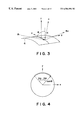
- FIG. 3 is a schematic view for explaining reflection of X-rays at a cylindrical surface of a reflection type integrator having convex cylindrical surfaces.
- FIG. 4 is a schematic view for explaining an angular distribution of X-rays reflected by a cylindrical surface of a reflection type integrator having cylindrical surfaces.
- FIG. 5 is a schematic view of an X-ray reduction projection exposure apparatus according to a first embodiment of the present invention.
- FIG. 6 is a schematic and perspective view of a reflection type integrator with convex cylindrical surfaces, usable in the first embodiment of the present invention.
- FIG. 7 is a schematic view for explaining an illumination region on the surface of a mask, in the first embodiment of the present invention.
- FIG. 8 is a schematic view of an X-ray reduction projection exposure apparatus according to a second embodiment of the present invention.
- FIG. 9 is a schematic and perspective view of a reflection type integrator with concave cylindrical surfaces, usable in the second embodiment of the present invention.
- FIG. 10 is a flow chart of microdevice manufacturing processes.
- FIG. 11 is a flow chart of a wafer process.
- FIG. 12 is a schematic view of an X-ray reduction projection exposure apparatus of a known type.
- FIG. 13 is a schematic and perspective view of a reflection type integrator of a known type.
- FIG. 14 is a schematic view for explaining an illumination region on the surface of a mask.
- FIG. 1 is a schematic and perspective view for explaining reflection of parallel light impinging on a reflection type integrator having convex cylindrical surfaces.
- FIG. 2 is a schematic and sectional view of the reflection type integrator having cylindrical surfaces.
- FIG. 3 is a schematic view for explaining reflection of X-rays at a cylindrical surface of a reflection type integrator having convex cylindrical surfaces.
- FIG. 4 is a schematic view for explaining an angular distribution of X-rays reflected by a cylindrical surface of a reflection type integrator having cylindrical surfaces.
- denoted at 5 is a reflection type integrator having convex cylindrical surfaces.
- An X-ray beam of substantially parallel light emitted from an X-ray light source is projected on the reflection type integrator 5 having a plurality of cylindrical surfaces, and secondary light sources are defined by this integrator.
- the X-rays emitted from these secondary light sources have an angular distribution of a conical surface shape.
- a reflector having a focal point placed at the secondary light source position reflects the X-rays to illuminate a mask.
- R 1 (0, ⁇ cos ⁇ , sin ⁇ )
- n ( ⁇ sin ⁇ , cos ⁇ , 0),
- R 2 (cos ⁇ sin 2 ⁇ , cos ⁇ cos 2 ⁇ , sin ⁇ ).
- the result is a circle of a radius cos ⁇ on an X-Y plane as shown in FIG. 4 . That is, the reflection light is formed into divergent light of a conical surface shape, and the secondary light source is located at the position of apex of this conical surface. If the cylindrical surface comprises a concave surface, the secondary light source is placed outside the reflection surface. If the cylindrical surface comprises a convex surface, the secondary light source is placed inside the reflection surface. Also, if the reflection surface is limitedly provided by a portion of a cylindrical surface and the central angle thereof is 2 ⁇ , then as shown in FIG. 4 the light ray vector of reflection light is arcuate with a central angle 4 ⁇ upon the X-Y plane.
- the light emitted from the secondary light source is divergent light and, after it is reflected by the reflection mirror of a focal length f, it is transformed into parallel light.
- the reflection light here is formed into a sheet beam of an arcuate sectional shape with a central angle 4 ⁇ , at a radius f ⁇ cos ⁇ .
- FIG. 1 While one cylindrical surface reflection mirror has been explained above, a cylindrical surface integrator such as shown in FIG. 1 will now be considered. That is, as shown, parallel light of a diameter D is projected on a reflection mirror of a wider area, having a number of cylindrical surfaces arrayed in parallel in a one-dimensional direction. If the reflection mirror and the mask are disposed in the same manner as in the foregoing example, the angular distribution of light reflected by the reflection mirror, with a number of cylindrical surfaces arrayed in parallel, is essentially the same as in the preceding case. Thus, an arcuate region on the mask with a radius f ⁇ cos ⁇ and a central angle 4 ⁇ is illuminated.
- the angular extension of it is D/f. That is, the numerical aperture of the illumination optical system is D/(2f). If the mask-side numerical aperture of the projection optical system is NAp 1 , the coherence factor is
- an optimum coherence factor ⁇ can be set.
- FIG. 5 is a schematic view of an X-ray reduction projection exposure apparatus according to a first embodiment of the present invention.
- FIG. 6 is a schematic and perspective view of a reflection type integrator with convex cylindrical surfaces, usable in the first embodiment of the present invention.
- FIG. 7 is a schematic view for explaining an illumination region on the surface of a mask, in the first embodiment of the present invention.
- Denoted in these drawings at 1 is a light emission point for X-rays, and denoted at 2 is an X-ray beam.
- Denoted at 3 is a filter, and denoted at 4 is a first rotational parabolic surface mirror.
- Denotod at 5 is a reflection type convex cylindrical surface integrator, and denoted at 6 is a second rotatational parabolic surface mirror.
- Denoted at 7 is a mask, and denoted at 8 is a projection optical system.
- Denoted at 9 is a wafer, and denoted at 10 is a mask stage.
- Denoted at 11 is a wafer stage, and denoted at 12 is an arcuate aperture.
- Denoted at 13 is a laser plasma X-ray light source, and denoted at 14 is a laser collecting optical system.
- Denoted at 15 is an illumination region on the mask surface, and denoted at 16 is an arcuate region through which the exposure is to be performed.
- Denoted at 17 is a vacuum chamber.
- the X-ray reduction projection exposure apparatus of the first embodiment of the preset invention comprises a laser plasma X-ray light source 13 , an illumination optical system, a mask 7 , a projection optical system 8 , a wafer 9 , stages 10 and 11 on which the mask or wafer is placed, an alignment mechanism for precisely aligning the positions of the mask and wafer, a vacuum chamber 17 for keeping the optical arrangement as a whole in a vacuum to prevent X-ray attenuation, and an evacuation device, for example.
- the illumination optical system comprises a first rotational parabolic surface mirror 4 , a reflection type convex cylindrical surface integrator 5 , and a second rotational parabolic surface mirror 6 .
- the mask 7 comprises a multilayered film reflection mirror on which a transfer pattern is defined by a non-reflective portion, provided by an X-ray absorptive material.
- the X-ray beam as reflected by the mask 7 is imaged by the projection optical system 8 upon the wafer 9 surface.
- the protection optical system 7 is so designed that good imaging performance is provided within a narrow arcuate region off the axis.
- the projection optical system 8 has two multilayered film reflection mirrors, and it serves to project the pattern of the mask 7 onto the wafer 9 in a reduced scale.
- the reduction magnification corresponds to the scan speed ratio between the mask and the wafer.
- the projection optical system 8 comprises a telecentric system.
- the X-ray beam 2 emitted from the light emission point 1 of the laser plasma X-ray source 13 passes a shield filter 3 of the target, for prevention of particle scattering, and it is reflected by the first rotational parabolic surface mirror 4 , whereby it is transformed into a parallel beam.
- This beam is then reflected by the reflection type integrator 5 with convex cylindrical surfaces, whereby a number of secondary light sources are produced.
- the X-rays from these secondary light sources are reflected by the second rotational parabolic surface mirror 6 , and they illuminate the mask 7 . Both of the distance from the secondary light source to the second rotational parabolic surface mirror 6 and the distance from the second parabolic surface mirror 6 to the mask 7 are equal to the focal length of the second rotational parabolic surface mirror.
- the reflection type convex cylindrical surface integrator 5 comprises a total reflection mirror having a shape that a number of small convex cylindrical surfaces are arrayed one-dimensionally such as shown in FIG. 6 .
- each arcuate portion has a radius of 0.5 mm and a central angle of 30 deg.
- the parallel X-ray beam has a thickness of 20 mm, and the incidence angle of the parallel X-ray beam upon-the integrator 5 is 85 deg.
- the mask 7 is disposed at a distance 2300 mm from the second rotational parabolic surface mirror 6 . Light emitted from one point on the secondary light source is divergent light having an angular distribution like a conical surface.
- this embodiment uses a reflection type convex cylindrical surface integrator 5 having a reflection surface provided by a number of small convex cylindrical surfaces arrayed one-dimensionally, by which the region on the mask 7 to be illuminated can be defined with an arcuate shape and, simultaneously, an optimum value for a coherence factor of the illumination optical system can be set. Also, the shape of the illumination region 15 on the mask 7 surface is restricted to the vicinity of the arcuate region 16 with which the exposure process is performed actually. Wasteful illumination of X-rays to a wide area outside the exposure region, such as shown in FIG. 14, is prevented. Thus, the loss of light quantity is reduced, the exposure time can be shortened and throughput can be improved.
- FIG. 8 is a schematic view of an X-ray reduction projection exposure apparatus according to a second embodiment of the present Invention.
- FIG. 9 is a schematic and perspective view of a reflection type integrator with concave cylindrical surfaces, usable in the second embodiment of the present invention.
- Denoted in these drawings at 801 is an undulator X-ray light source, and denoted at 802 is an X-ray beam.
- Denoted at 803 is a convex surface mirror, and denoted at 804 is a first concave surface mirror.
- Denoted at 805 is a reflection type integrator with concave cylindrical surfaces, and denoted at 806 is a second concave surface mirror
- Denoted at 807 is a mask
- denoted at 808 is a projection optical system.
- Denoted at 809 is a wafer.
- Denoted at 810 is a mask stage, and denoted at 811 is a wafer stage.
- Denoted at 812 is an arcuate aperture, and denoted at 817 is a vacuum chamber.
- the X-ray reduction projection exposure apparatus comprises an undulator X-ray light source 801 , an illumination optical system, a mask 807 , a projection optical system 808 , a wafer 809 , stages 810 and 811 having the mask or wafer placed thereon, an alignment mechanism for precisely aligning the positions of the mask and wafer, a vacuum chamber for keeping the optical arrangement as a whole in a vacuum for prevention of X-ray attenuation, and an evacuation device, for example.
- the mask 807 comprises a multilayered film reflection mirror on which a transfer pattern is defined by a non-reflective portion, provided by an X-ray absorptive material.
- the X-ray beam as reflected by the mask 807 is imaged by the projection optical system 808 upon the wafer 809 surface.
- the projection optical system 808 is so designed that good imaging performance is provided in a narrow arcuate region off the axis. In order that the exposure process is performed only by use of this narrow arcuate region, an aperture 812 having an arcuate opening is disposed just before the wafer 809 .
- the projection optical system 808 has three multilayered film reflection mirrors, and it serves to project the pattern of the mask 807 onto the wafer 809 in a reduced scale.
- the X-ray beam 802 emitted from the light emission point of the undulator X-ray light source 801 is a narrow and substantially parallel beam. It is reflected by the convex surface mirror 803 and the first concave surface mirror 804 , whereby it is transformed into a thick parallel beam. This beam is reflected by the reflection type concave cylindrical surface integrator 805 of the structure that concave cylindrical surfaces with multilayered films for increased X-ray reflectivity are arrayed in parallel. By this, a number of secondary light sources are produced. Light emitted from a single point on the secondary light source is divergent light of a conical surface shape and, after being reflected by the second concave surface mirror 806 , it is transformed into parallel light. Then, an arcuate region on the mask 807 is illuminated.
- this embodiment uses a reflection type concave cylindrical surface integrator 805 having a number of small concave cylindrical surfaces arrayed one-dimensionally, by which the region on the mask 807 to be illuminated can be made arcuate and, additionally, an optimum value for the coherence factor of the illumination optical system can be set. Also, the shape of the illumination region on the mask 807 surface is restricted to an arcuate region with which the exposure is to be done actually. Wasteful X-ray illumination to those areas outside the exposure region is prevented. Thus, the loss of light quantity is reduced, the exposure time can be shortened and the throughput can be improved.
- the X-ray illumination optical system and X-ray reduction exposure apparatus described above assure, with use of a reflection type integrator having a reflection mirror of a wide area provided by a number of cylindrical surfaces arrayed in parallel, illumination of only an arcuate region on a mask. Also, it enables setting the numerical aperture of the illumination system to provide an optimum coherent factor ⁇ .
- the shape of the illumination region on the mask is restricted to an arcuate region with which the exposure is to be done actually, and wasteful X-ray illumination to those areas other than the exposure region is prevented.
- loss of light quantity is reduced, the exposure time can be shortened and the throughput can be enhanced.
- the reflection surface of the reflection type integrator may be provided with a multilayered film, to provide higher X-ray reflectivity.
- FIG. 10 is a flow chart of a procedure for the manufacture of microdevices such as semiconductor chips (e.g., ICs or LSIs), liquid crystal panels, and CCDs, for example.
- Step 1 is a design process for designing a circuit of a semiconductor device.
- Step 2 is a process for making a mask on the basis of the circuit pattern design.
- Step 3 is a process for preparing a wafer by using a material such as silicon.
- Step 4 is a wafer process which is called a pre-process wherein, by using the so prepared mask and wafer, circuits are practically formed on the wafer through lithography.
- Step 5 subsequent to this is an assembling step which is called a post-process wherein the wafer having been processed by step 4 is formed into semiconductor chips.
- This step includes an assembling (dicing and bonding) process and a packaging (chip sealing) process.
- Step 6 is an inspection step wherein an operation check, a durability check and so on for the semiconductor devices provided by step 5 , are carried out. With these processes, semiconductor devices are completed and they are shipped (step 7 ).
- FIG. 11 is a flow chart showing details of the wafer process.
- Step 11 is an oxidation process for oxidizing the surface of a wafer.
- Step 12 is a CVD process for forming an insulating film on the wafer surface.
- Step 13 is an electrode forming process for forming electrodes upon the wafer by vapor deposition.
- Step 14 is an ion implanting process for implanting ions to the wafer.
- Step 15 is a resist process for applying a resist (photosensitive material) to the wafer.
- Step 16 is an exposure process for printing, by exposure, the circuit pattern of the mask on the wafer through the exposure apparatus described above.
- Step 17 is a developing process for developing the exposed wafer.
- Step 18 is an etching process for removing portions other than the developed resist image.
- Step 19 is a resist separation process for separating the resist material remaining on the wafer after being subjected to the etching process. By repeating these processes, circuit patterns are superposedly formed on the wafer.
Landscapes
- Physics & Mathematics (AREA)
- Spectroscopy & Molecular Physics (AREA)
- Engineering & Computer Science (AREA)
- General Engineering & Computer Science (AREA)
- High Energy & Nuclear Physics (AREA)
- General Physics & Mathematics (AREA)
- Exposure Of Semiconductors, Excluding Electron Or Ion Beam Exposure (AREA)
- Exposure And Positioning Against Photoresist Photosensitive Materials (AREA)
Priority Applications (2)
| Application Number | Priority Date | Filing Date | Title |
|---|---|---|---|
| US10/119,707 US6834098B2 (en) | 1996-08-26 | 2002-04-11 | X-ray illumination optical system and X-ray reduction exposure apparatus |
| US10/930,746 US7133489B2 (en) | 1996-08-26 | 2004-09-01 | X-ray illumination optical system and X-ray reduction exposure apparatus |
Applications Claiming Priority (3)
| Application Number | Priority Date | Filing Date | Title |
|---|---|---|---|
| JP22361496A JP3706691B2 (ja) | 1996-08-26 | 1996-08-26 | X線縮小投影露光装置及びこれを用いた半導体デバイス製造方法 |
| JP8-223614 | 1996-08-26 | ||
| JP223614/1996 | 1996-08-26 |
Related Child Applications (1)
| Application Number | Title | Priority Date | Filing Date |
|---|---|---|---|
| US10/119,707 Continuation US6834098B2 (en) | 1996-08-26 | 2002-04-11 | X-ray illumination optical system and X-ray reduction exposure apparatus |
Publications (2)
| Publication Number | Publication Date |
|---|---|
| US20020003855A1 US20020003855A1 (en) | 2002-01-10 |
| US6504896B2 true US6504896B2 (en) | 2003-01-07 |
Family
ID=16800967
Family Applications (3)
| Application Number | Title | Priority Date | Filing Date |
|---|---|---|---|
| US08/917,373 Expired - Fee Related US6504896B2 (en) | 1996-08-26 | 1997-08-26 | X-ray illumination optical system and x-ray reduction exposure apparatus |
| US10/119,707 Expired - Fee Related US6834098B2 (en) | 1996-08-26 | 2002-04-11 | X-ray illumination optical system and X-ray reduction exposure apparatus |
| US10/930,746 Expired - Fee Related US7133489B2 (en) | 1996-08-26 | 2004-09-01 | X-ray illumination optical system and X-ray reduction exposure apparatus |
Family Applications After (2)
| Application Number | Title | Priority Date | Filing Date |
|---|---|---|---|
| US10/119,707 Expired - Fee Related US6834098B2 (en) | 1996-08-26 | 2002-04-11 | X-ray illumination optical system and X-ray reduction exposure apparatus |
| US10/930,746 Expired - Fee Related US7133489B2 (en) | 1996-08-26 | 2004-09-01 | X-ray illumination optical system and X-ray reduction exposure apparatus |
Country Status (2)
| Country | Link |
|---|---|
| US (3) | US6504896B2 (ja) |
| JP (1) | JP3706691B2 (ja) |
Cited By (14)
| Publication number | Priority date | Publication date | Assignee | Title |
|---|---|---|---|---|
| US20020131181A1 (en) * | 2001-01-08 | 2002-09-19 | Wolfgang Singer | Illumination system with raster elements of different sizes |
| US20030031017A1 (en) * | 2001-07-27 | 2003-02-13 | Toshihiko Tsuji | Illumination system, projection exposure apparatus and device manufacturing method |
| US20030035091A1 (en) * | 2001-08-13 | 2003-02-20 | Michio Kohno | Illumination apparatus, projection exposure apparatus, and device fabricating method |
| US20030142410A1 (en) * | 2002-01-29 | 2003-07-31 | Canon Kabushiki Kaisha | Exposure apparatus, control method thereof, and device manufacturing method using the same |
| US20030142198A1 (en) * | 2002-01-29 | 2003-07-31 | Canon Kabushiki Kaisha | Plasma light source apparatus, exposure apparatus and its control method and device fabrication method |
| US20030179377A1 (en) * | 2002-03-20 | 2003-09-25 | Canon Kabushiki Kaisha | Mirror device, mirror adjustment method, exposure apparatus, exposure method, and semiconductor device manufacturing method |
| US6842500B1 (en) * | 1998-09-17 | 2005-01-11 | Nikon Corporation | Exposure apparatus and exposure method using same |
| US20050031072A1 (en) * | 1996-08-26 | 2005-02-10 | Canon Kabushiki Kaisha | X-ray illumination optical system and x-ray reduction exposure apparatus |
| US20050057738A1 (en) * | 2003-09-17 | 2005-03-17 | Toshihiko Tsuji | Illumination optical system and exposure apparatus |
| US20050105290A1 (en) * | 2003-11-10 | 2005-05-19 | Canon Kabushiki Kaisha | Illumination optical system and exposure apparatus |
| US20050247684A1 (en) * | 2004-05-06 | 2005-11-10 | Semiconductor Energy Laboratory Co., Ltd. | Laser irradiation apparatus |
| US7083290B2 (en) | 2002-07-29 | 2006-08-01 | Canon Kabushiki Kaisha | Adjustment method and apparatus of optical system, and exposure apparatus |
| US20070071164A1 (en) * | 2005-09-29 | 2007-03-29 | The University Of Chicago | Optomechanical structure for a multifunctional hard x-ray nanoprobe instrument |
| US20090027641A1 (en) * | 2007-07-27 | 2009-01-29 | Canon Kabushiki Kaisha | Illumination optical system and exposure apparatus including the same |
Families Citing this family (9)
| Publication number | Priority date | Publication date | Assignee | Title |
|---|---|---|---|---|
| US6898216B1 (en) * | 1999-06-30 | 2005-05-24 | Lambda Physik Ag | Reduction of laser speckle in photolithography by controlled disruption of spatial coherence of laser beam |
| TWI243287B (en) * | 1999-03-12 | 2005-11-11 | Asml Netherlands Bv | Lithographic projection apparatus and device manufacturing method using the same |
| JP3720788B2 (ja) | 2002-04-15 | 2005-11-30 | キヤノン株式会社 | 投影露光装置及びデバイス製造方法 |
| WO2004068564A1 (ja) * | 2002-12-26 | 2004-08-12 | Nikon Corporation | 照明光学系、照明装置、投影露光装置、及び露光方法 |
| KR101273740B1 (ko) | 2004-09-22 | 2013-06-12 | 가부시키가이샤 니콘 | 조명 장치, 노광 장치 및 마이크로 디바이스의 제조 방법 |
| JP2006253487A (ja) * | 2005-03-11 | 2006-09-21 | Nikon Corp | 照明装置、投影露光方法、投影露光装置、及びマイクロデバイスの製造方法 |
| JP5241270B2 (ja) * | 2008-02-27 | 2013-07-17 | キヤノン株式会社 | 照明光学系、これを用いた露光装置及びデバイス製造方法 |
| JP5142892B2 (ja) * | 2008-09-03 | 2013-02-13 | キヤノン株式会社 | 照明光学系及び露光装置 |
| US8518894B2 (en) * | 2009-06-01 | 2013-08-27 | Kenneth James Friel | Human milk peptides |
Citations (1)
| Publication number | Priority date | Publication date | Assignee | Title |
|---|---|---|---|---|
| US5677939A (en) * | 1994-02-23 | 1997-10-14 | Nikon Corporation | Illuminating apparatus |
Family Cites Families (5)
| Publication number | Priority date | Publication date | Assignee | Title |
|---|---|---|---|---|
| JP3210143B2 (ja) * | 1992-07-20 | 2001-09-17 | キヤノン株式会社 | X線マスク構造体とその作製方法、及び、該x線マスク構造体を用いたx線露光方法と、該x線マスク構造体を用いて作成するデバイス製造方法 |
| JP3254771B2 (ja) * | 1992-12-10 | 2002-02-12 | 株式会社ニコン | X線縮小投影露光装置および方法 |
| JP3371510B2 (ja) * | 1994-02-23 | 2003-01-27 | 株式会社ニコン | 照明装置及び露光装置 |
| JP3521506B2 (ja) * | 1994-11-24 | 2004-04-19 | 株式会社ニコン | 照明装置及び露光装置 |
| JP3706691B2 (ja) * | 1996-08-26 | 2005-10-12 | キヤノン株式会社 | X線縮小投影露光装置及びこれを用いた半導体デバイス製造方法 |
-
1996
- 1996-08-26 JP JP22361496A patent/JP3706691B2/ja not_active Expired - Fee Related
-
1997
- 1997-08-26 US US08/917,373 patent/US6504896B2/en not_active Expired - Fee Related
-
2002
- 2002-04-11 US US10/119,707 patent/US6834098B2/en not_active Expired - Fee Related
-
2004
- 2004-09-01 US US10/930,746 patent/US7133489B2/en not_active Expired - Fee Related
Patent Citations (1)
| Publication number | Priority date | Publication date | Assignee | Title |
|---|---|---|---|---|
| US5677939A (en) * | 1994-02-23 | 1997-10-14 | Nikon Corporation | Illuminating apparatus |
Cited By (26)
| Publication number | Priority date | Publication date | Assignee | Title |
|---|---|---|---|---|
| US7133489B2 (en) * | 1996-08-26 | 2006-11-07 | Canon Kabushiki Kaisha | X-ray illumination optical system and X-ray reduction exposure apparatus |
| US20050031072A1 (en) * | 1996-08-26 | 2005-02-10 | Canon Kabushiki Kaisha | X-ray illumination optical system and x-ray reduction exposure apparatus |
| US6842500B1 (en) * | 1998-09-17 | 2005-01-11 | Nikon Corporation | Exposure apparatus and exposure method using same |
| US20020131181A1 (en) * | 2001-01-08 | 2002-09-19 | Wolfgang Singer | Illumination system with raster elements of different sizes |
| US7400699B2 (en) * | 2001-01-08 | 2008-07-15 | Carl Zeiss Smt Ag | Illumination system with raster elements of different sizes |
| US20030031017A1 (en) * | 2001-07-27 | 2003-02-13 | Toshihiko Tsuji | Illumination system, projection exposure apparatus and device manufacturing method |
| US6919951B2 (en) * | 2001-07-27 | 2005-07-19 | Canon Kabushiki Kaisha | Illumination system, projection exposure apparatus and device manufacturing method |
| US20030035091A1 (en) * | 2001-08-13 | 2003-02-20 | Michio Kohno | Illumination apparatus, projection exposure apparatus, and device fabricating method |
| US6833905B2 (en) | 2001-08-13 | 2004-12-21 | Canon Kabushiki Kaisha | Illumination apparatus, projection exposure apparatus, and device fabricating method |
| US20030142410A1 (en) * | 2002-01-29 | 2003-07-31 | Canon Kabushiki Kaisha | Exposure apparatus, control method thereof, and device manufacturing method using the same |
| US6825481B2 (en) | 2002-01-29 | 2004-11-30 | Canon Kabushiki Kaisha | Exposure apparatus, control method thereof, and device manufacturing method using the same |
| US20030142198A1 (en) * | 2002-01-29 | 2003-07-31 | Canon Kabushiki Kaisha | Plasma light source apparatus, exposure apparatus and its control method and device fabrication method |
| US6831744B2 (en) | 2002-03-20 | 2004-12-14 | Canon Kabushiki Kaisha | Mirror device, mirror adjustment method, exposure apparatus, exposure method, and semiconductor device manufacturing method |
| US20030179377A1 (en) * | 2002-03-20 | 2003-09-25 | Canon Kabushiki Kaisha | Mirror device, mirror adjustment method, exposure apparatus, exposure method, and semiconductor device manufacturing method |
| US7083290B2 (en) | 2002-07-29 | 2006-08-01 | Canon Kabushiki Kaisha | Adjustment method and apparatus of optical system, and exposure apparatus |
| US20050057737A1 (en) * | 2003-09-17 | 2005-03-17 | Toshihiko Tsuji | Illumination optical system and exposure apparatus |
| US7064806B2 (en) | 2003-09-17 | 2006-06-20 | Canon Kabushiki Kaisha | Illumination optical system and exposure apparatus |
| US7110084B2 (en) | 2003-09-17 | 2006-09-19 | Canon Kabushiki Kaisha | Illumination optical system and exposure apparatus |
| US20050057738A1 (en) * | 2003-09-17 | 2005-03-17 | Toshihiko Tsuji | Illumination optical system and exposure apparatus |
| US20050105290A1 (en) * | 2003-11-10 | 2005-05-19 | Canon Kabushiki Kaisha | Illumination optical system and exposure apparatus |
| US20050247684A1 (en) * | 2004-05-06 | 2005-11-10 | Semiconductor Energy Laboratory Co., Ltd. | Laser irradiation apparatus |
| US8525075B2 (en) * | 2004-05-06 | 2013-09-03 | Semiconductor Energy Laboratory Co., Ltd. | Laser irradiation apparatus |
| US20070071164A1 (en) * | 2005-09-29 | 2007-03-29 | The University Of Chicago | Optomechanical structure for a multifunctional hard x-ray nanoprobe instrument |
| US7331714B2 (en) * | 2005-09-29 | 2008-02-19 | Uchicago Argonne, Llc | Optomechanical structure for a multifunctional hard x-ray nanoprobe instrument |
| US20090027641A1 (en) * | 2007-07-27 | 2009-01-29 | Canon Kabushiki Kaisha | Illumination optical system and exposure apparatus including the same |
| US7538856B2 (en) * | 2007-07-27 | 2009-05-26 | Canon Kabushiki Kaisha | Illumination optical system and exposure apparatus including the same |
Also Published As
| Publication number | Publication date |
|---|---|
| JPH1070058A (ja) | 1998-03-10 |
| JP3706691B2 (ja) | 2005-10-12 |
| US6834098B2 (en) | 2004-12-21 |
| US20020110217A1 (en) | 2002-08-15 |
| US20050031072A1 (en) | 2005-02-10 |
| US20020003855A1 (en) | 2002-01-10 |
| US7133489B2 (en) | 2006-11-07 |
Similar Documents
| Publication | Publication Date | Title |
|---|---|---|
| US6834098B2 (en) | X-ray illumination optical system and X-ray reduction exposure apparatus | |
| US5995582A (en) | X-ray reduction exposure apparatus and device manufacturing method using the same | |
| US6885432B2 (en) | Projection exposure apparatus and device manufacturing method | |
| US6919951B2 (en) | Illumination system, projection exposure apparatus and device manufacturing method | |
| JP3284045B2 (ja) | X線光学装置およびデバイス製造方法 | |
| CA2080083C (en) | Optical arrangement for exposure apparatus | |
| US5719617A (en) | Illumination system for superposing light beams one upon another on a surface using a projecting system having different focal point positions | |
| US6639652B1 (en) | Illumination system for use in exposure apparatus | |
| US6857764B2 (en) | Illumination optical system and exposure apparatus having the same | |
| KR100917418B1 (ko) | 노광장치 | |
| JP3605055B2 (ja) | 照明光学系、露光装置及びデバイス製造方法 | |
| US6285440B1 (en) | Illumination system and projection exposure apparatus using the same | |
| US5127029A (en) | X-ray exposure apparatus | |
| JP2005093693A (ja) | 露光装置 | |
| JP3618856B2 (ja) | X線露光装置、及びこれを用いたデバイス生産方法 | |
| US6055039A (en) | Illumination system and exposure apparatus using the same | |
| JP3371510B2 (ja) | 照明装置及び露光装置 | |
| JP3618853B2 (ja) | X線発生装置、及びこれを用いた露光装置やデバイス生産方法 | |
| JP3715984B2 (ja) | X線縮小投影露光方法、x線縮小投影露光装置及びこれを用いた半導体デバイス製造方法 | |
| JP3336514B2 (ja) | X線反射型マスク及びx線投影露光装置 | |
| JP3165744B2 (ja) | 露光装置などの光学装置、及び半導体デバイス製造方法 | |
| JPH0774083A (ja) | 露光用原板及びそれを用いた投影露光装置 | |
| JPH06177014A (ja) | X線縮小投影露光装置 |
Legal Events
| Date | Code | Title | Description |
|---|---|---|---|
| AS | Assignment |
Owner name: CANON KABUSHIKI KAISHA, JAPAN Free format text: ASSIGNMENT OF ASSIGNORS INTEREST;ASSIGNORS:MIYAKE, AKIRA;TSUKAMOTO, MASAMI;REEL/FRAME:009045/0263 Effective date: 19980216 |
|
| CC | Certificate of correction | ||
| FPAY | Fee payment |
Year of fee payment: 4 |
|
| FPAY | Fee payment |
Year of fee payment: 8 |
|
| REMI | Maintenance fee reminder mailed | ||
| LAPS | Lapse for failure to pay maintenance fees | ||
| STCH | Information on status: patent discontinuation |
Free format text: PATENT EXPIRED DUE TO NONPAYMENT OF MAINTENANCE FEES UNDER 37 CFR 1.362 |
|
| FP | Lapsed due to failure to pay maintenance fee |
Effective date: 20150107 |