US6554906B1 - Wafer holder for semiconductor manufacturing apparatus and semiconductor manufacturing apparatus using the same - Google Patents
Wafer holder for semiconductor manufacturing apparatus and semiconductor manufacturing apparatus using the same Download PDFInfo
- Publication number
- US6554906B1 US6554906B1 US09/707,813 US70781300A US6554906B1 US 6554906 B1 US6554906 B1 US 6554906B1 US 70781300 A US70781300 A US 70781300A US 6554906 B1 US6554906 B1 US 6554906B1
- Authority
- US
- United States
- Prior art keywords
- manufacturing apparatus
- semiconductor manufacturing
- wafer holder
- ceramic base
- wafer
- Prior art date
- Legal status (The legal status is an assumption and is not a legal conclusion. Google has not performed a legal analysis and makes no representation as to the accuracy of the status listed.)
- Expired - Fee Related, expires
Links
Images


Classifications
-
- H—ELECTRICITY
- H10—SEMICONDUCTOR DEVICES; ELECTRIC SOLID-STATE DEVICES NOT OTHERWISE PROVIDED FOR
- H10P—GENERIC PROCESSES OR APPARATUS FOR THE MANUFACTURE OR TREATMENT OF DEVICES COVERED BY CLASS H10
- H10P72/00—Handling or holding of wafers, substrates or devices during manufacture or treatment thereof
- H10P72/50—Handling or holding of wafers, substrates or devices during manufacture or treatment thereof for positioning, orientation or alignment
-
- H—ELECTRICITY
- H10—SEMICONDUCTOR DEVICES; ELECTRIC SOLID-STATE DEVICES NOT OTHERWISE PROVIDED FOR
- H10P—GENERIC PROCESSES OR APPARATUS FOR THE MANUFACTURE OR TREATMENT OF DEVICES COVERED BY CLASS H10
- H10P72/00—Handling or holding of wafers, substrates or devices during manufacture or treatment thereof
- H10P72/04—Apparatus for manufacture or treatment
- H10P72/0431—Apparatus for thermal treatment
- H10P72/0432—Apparatus for thermal treatment mainly by conduction
Definitions
- the present invention relates generally to wafer holders for semiconductor manufacturing apparatus and semiconductor manufacturing apparatus using the same and particularly to wafer holders for semiconductor manufacturing apparatus having a heater for heating a wafer, an electrode for an electrostatic chuck electrostatically holding a wafer or the functions of both of such heater and electrode, and semiconductor manufacturing apparatus using the same.
- etching a surface of a semiconductor wafer or depositing a film thereon a multitude of such wafers are held on a rack and batch-processed, exposed to an etchant gas or a gas for deposition, and circumferentially heated with a heater, as required.
- This technique is referred to as hot-wall technique.
- the loader transfers a wafer to an etching apparatus or a deposition apparatus and places the wafer in a chamber therein on a holder holding the wafer by means of an electrostatic chuck or alternatively on a holder's wafer bearing side having a surface increased in precision so that the wafer can be placed still on and in close contact with the holder and the holder thus heats the wafer directly to heat the wafer uniformly.
- the holder needs to at least have a portion in contact with a wafer that is formed of a material resistant to a highly corrosive gas such as halogen gas and highly heat-conducting, and the holder per se also needs to function to electrostatically chuck, mechanically fix and heat a wafer.
- a material having been noted as a material used for forming the holder is aluminum nitride, which is resistant to corrosion and highly heat-conducting. Powdery aluminum nitride is molded to provide media formed thereof and therebetween a coil or wire of a refractory metal such as Mo is interposed and they are then hot-pressed and thus sintered to embed a conductive layer used for a heater, an electrostatic chuck or the like.
- a refractory metal such as Mo
- Japanese Patent Publication No. 2604944 discloses a configuration with an embedded heater allowing a heat emitting side to provide more uniform heat.
- a molded medium formed of aluminum nitride and having a surface printed with a paste containing W, Mo or the like is placed on another medium and the aluminum nitride is sintered to provide a holder having a conductive layer embedded therein.
- a heater or an electrostatic chuck is powered, as described with reference to FIG. 19 .
- a ceramic base member 104 has a back side provided with a pipe bonded thereto and accommodating therein extraction lines 107 A and 107 B externally feeding power to each of conductive layers 101 and 102 serving as the heater or the electrostatic chuck.
- the holder in the form of a disc and pipe 106 for accommodating the extraction lines must be manufactured separately and to bond holder 110 and pipe 106 together a bonding glass must be initially applied and diffusion-bonding or the like must be then employed, which is a cumbersome process.
- holder 110 having a back side with a pipe bonded thereto would have front and back surfaces having different levels of heat dissipation.
- the front side and the back side would have therebetween a difference in temperature and holder 110 would thus distort when it is heated or cooled.
- holder 110 distorted would provide a gap between the holder and the wafer. This would result in uneven heat transfer which would then cause a variation in the temperature of the wafer's surface and hence an uneven etch rate and an uneven deposition rate in the wafer's plane.
- the holder should be formed of a plate at least 5 mm thick, which would increase the cost for its source material(s).
- bonding pipe 106 would increase the thermal capacity and if holder 110 is adapted to also function as a heater then it would require a long period of time to heat and cool the holder. Furthermore, in fabricating the pipe when the pipe molded has a binder heated and thus removed therefrom the binder is hard to remove and the pipe can thus break and the pipe tends to be unevenly sintered or deform when it is sintered so that the binder should be removed over a long period of time and furthermore the sintering charge level reduces, which significantly increases the production cost.
- this structure entails joining at an end of pipe 106 .
- the area for the joint should be considered to maintain the anti-leakage level as required and pipe 106 is thus required to have an increased diameter.
- pipe 106 is also required to support holder 110 , pipe 106 is also forced to have an increased diameter, resulting in the same disadvantage as described above.
- the present invention contemplates a wafer holder for use with a semiconductor manufacturing apparatus that can reduce such distortion as caused when it is heated and cooled and that can also be readily manufactured, and a semiconductor manufacturing apparatus employing the same.
- the present invention in one aspect provides a wafer holder for use with a semiconductor manufacturing apparatus, including a conductive layer and a pair of ceramic base members sandwiching the conductive layer therebetween, wherein the conductive layer has a body located at a surface opposite a wafer holding surface of one of the ceramic base members and an extension protruding radially from the body to the outside of a vacuum chamber for external electrical connection, and the body and the extension are arranged substantially in a single plane.
- the extension is also referred to as an “extraction”.
- the present invention in one aspect provides a wafer holder for a semiconductor manufacturing apparatus including a conductive layer having a body and an extension or extraction provided in a single plane, the body and the extraction can be both posed and thus protected between paired ceramic base members each in the form of a flat plate.
- This can eliminate the necessity of using a pipe for protecting the extraction, as conventional, and hence the necessity of providing the step of bonding the pipe.
- the wafer holder can be readily manufactured and also free of such distortion as attributed to bonding such pipe.
- the wafer holder preferably includes the ceramic base member formed of at least one material selected from the group consisting of aluminum nitride, silicon nitride, aluminum nitride oxide and aluminum oxide.
- a material resistant to corrosion and having a high heat conductance can be appropriately selected as the ceramic base member.
- the wafer holder preferably includes the ceramic base members having a heat conductance of no less than 100 W/mK.
- the wafer holder can be improved in heat uniformity to process a wafer more rapidly.
- the wafer holder preferably includes the conductive layer and the ceramic base member with an intermediate layer posed therebetween and formed of a material including at least one of glass having a thermal expansion coefficient of at least 3 ⁇ 10 ⁇ 6 /°C. and at most 8 ⁇ 10 ⁇ 6/°C. and nonoxide ceramic having a thermal expansion coefficient of at least 3 ⁇ 10 ⁇ 6 /°C. and at most 6 ⁇ 10 ⁇ 6 /°C.
- the thermal expansion coefficient ranged as above can satisfy the requirement that the wafer holder should be heated from a room temperature to 600° C. within 30 minutes.
- the intermediate layer containing nonoxide ceramic allows the wafer holder heated to a high temperature and receiving a high level of voltage to be satisfactorily resistant to heat, corrosion and voltage.
- the wafer holder preferably has the intermediate layer containing nonoxide ceramic containing at least 50% by mass of aluminum nitride or silicon nitride.
- the nonoxide ceramic corresponding to aluminum nitride or silicon nitride allows the wafer holder heated to a high temperature and receiving a high level of voltage to be further satisfactorily resistant to heat, corrosion and voltage.
- the wafer holder preferably has the intermediate layer formed of a material including an oxide containing ytterbium, neodymium and calcium or a compound producing an oxide containing ytterbium, neodymium and calcium when heat treatment is performed.
- the intermediate layer can have a satisfactory wettability and bond performance.
- the wafer holder preferably has the intermediate layer formed of a material containing an oxide containing yttrium and aluminum or a compound producing an oxide containing yttrium and aluminum when heat treatment is performed.
- the intermediate layer can have a satisfactory wettability and bond performance.
- the wafer holder preferably includes the ceramic base member having a hole formed therein for arranging a temperature detection unit therein.
- the hole elongate to introduce the temperature detection unit from the side plate portion into the body to reach a predetermined position, can be readily formed by providing one or both of the substrates with a groove and then bonding them together.
- the wafer holder preferably includes the pair rap of ceramic base members having their respective wafer holding portions sandwiching the body and their respective side plate portions each extending from a side surface of the wafer holding portion and together sandwiching the extraction, and having a width smaller than a width of the wafer holding portion.
- the heat of the wafer holding portion can be prevented from dissipating to the side plate portion.
- the wafer holding portion can be rapidly heated to process a wafer more rapidly.
- the wafer holder preferably includes the conductive layer at least having the body formed of a material formed of at least one element selected from the group consisting of W, Mo, Ag, Pd, Pt, Ni and Cr.
- the conductive layer can be formed of a material appropriately selected suitable for the production.
- the wafer holder preferably includes the conductive layer corresponding to any one of a heater, an electrode for generating a plasma and an electrode for an electrostatic chuck.
- the electrode for generating a plasma and the electrode for an electrostatic chuck no pipe is required in protecting an extraction.
- the wafer holder preferably has a total thickness of no more than 5 mm.
- the wafer holder can heat and cool and thus process a wafer rapidly.
- the wafer holder preferably includes the conductive layer formed of a wire.
- the present invention can also be applied to a wafer holder including a conductive layer formed of a wire.
- the wafer holder is preferably provided with an O-ring arranged on and extending around the side plate portions of the pair of ceramic base members sandwiching the extraction.
- the vacuum chamber can maintain its internal vacuum.
- the wafer holder is preferably provided with a heat insulating neck provided in at least one of the side plate portions of the pair of ceramic base members sandwiching the extraction.
- the side plate portion can effectively insulate heat to prevent heat from dissipating from the wafer holding portion to the side plate portion.
- the wafer holding portion can be improved in heat uniformity
- the O ring attached to the side plate portion can be free of thermal degradation
- the side plate portion can be reduced in length.
- the wafer holder is preferably provided with the heater having its body in a region sandwiched between the side plate portions of the pair of ceramic base members.
- the side plate portion readily allowing heat to dissipate, can also emit heat to prevent the side plate portion and therearound from being cooled.
- the present invention in one aspect provides a semiconductor manufacturing apparatus having incorporated therein the above wafer holder for use with a semiconductor manufacturing apparatus.
- a semiconductor manufacturing apparatus having a wafer holder for use with a semiconductor manufacturing apparatus that can be prevented from distorting when it is heated and cooled and that can also be readily manufactured.
- the semiconductor manufacturing apparatus is preferably either one of an etching apparatus, a chemical vapor deposition apparatus and a plasma chemical vapor deposition apparatus.
- an etching apparatus a CVD apparatus and a plasma CVD apparatus having a wafer holder for use with a semiconductor manufacturing apparatus that can be prevented from distorting when it is heated and cooled and that can also be readily manufactured.
- the present invention in another aspect provides a wafer holder for a semiconductor manufacturing apparatus, including a ceramic base member, a conductive layer provided on the ceramic base member and a protection layer covering the conductive layer, wherein the conductive layer has a body facing a wafer holding surface of the ceramic base member and an extraction extracted from the body for external connection and the body and the extraction are arranged substantially in a single plane.
- the present invention in one aspect provides a wafer holder for use with a semiconductor manufacturing apparatus including a conductive layer having a body and an extraction provided in a single plane, covering with the protection layer can protect the conductive layer.
- This can eliminate the necessity of using a pipe for protecting the extraction, as conventional, and hence the necessity of providing the step of bonding the pipe.
- the wafer holder can be readily manufactured and also free of such distortion as attributed to bonding such pipe.
- the wafer holder preferably includes the ceramic base member formed of at least one material selected from the group consisting of aluminum nitride, silicon nitride, aluminum nitride oxide and aluminum oxide.
- a material resistant to corrosion and having a high heat conductance can be appropriately selected as the ceramic base member.
- the wafer holder preferably includes the ceramic base member having a heat conductance of no less than 100 W/mK.
- the wafer holder can be improved in heat uniformity to process a wafer more rapidly.
- the wafer holder preferably includes the protection layer formed of a material including at least one of glass having a thermal expansion coefficient of at least 3 ⁇ 10 ⁇ 6 /°C. and at most 8 ⁇ 10 ⁇ 6 /°C. and nonoxide ceramic having a thermal expansion coefficient of at least 3 ⁇ 10 ⁇ 6 /°C. and at most 6 ⁇ 10 ⁇ 6 /°C.
- the thermal expansion coefficient ranged as above can satisfy the requirement that the wafer holder should be heated from a room temperature to 600° C. within 30 minutes.
- the protection layer containing nonoxide ceramic allows the wafer holder having a high temperature and receiving a high level of voltage to be satisfactorily resistant to heat, corrosion and voltage.
- the wafer holder preferably has the protection layer containing nonoxide ceramic containing at least 50% by mass of aluminum nitride or silicon nitride.
- the nonoxide ceramic corresponding to aluminum nitride or silicon nitride allows the wafer holder having a high temperature and receiving a high level of voltage to be further satisfactorily resistant to heat, corrosion and voltage.
- the wafer holder preferably has the protection layer formed of a material including an oxide containing ytterbium, neodymium and calcium or a compound producing an oxide containing ytterbium, neodymium and calcium when heat treatment is performed.
- the protection layer can have a satisfactory wettability and bond performance.
- the wafer holder preferably has the protection layer formed of a material containing an oxide containing yttrium and aluminum or a compound producing an oxide containing yttrium and aluminum when heat treatment is performed.
- the intermediate layer can have a satisfactory wettability and bond performance.
- the wafer holder preferably includes the ceramic base member having a hole formed therein for arranging a temperature detection unit therein.
- the hole elongate to introduce the temperature detection unit from the side plate portion into the body to reach a predetermined position, can be readily formed by providing one or both of the substrates with a groove and then bonding them together.
- the wafer holder preferably includes the conductive layer at least having the body formed of a material formed of at least one element selected from the group consisting of W, Mo, Ag, Pd, Pt, Ni and Cr.
- the conductive layer can be formed of a material appropriately selected suitable for the production.
- the wafer holder preferably includes the conductive layer corresponding to any one of a heater, an electrode for generating a plasma and an electrode for an electrostatic chuck.
- the electrode for generating a plasma and the electrode for an electrostatic chuck no pipe is required in protecting an extraction.
- the wafer holder preferably has a total thickness of no more than 5 mm.
- the wafer holder can heat and cool and thus process a wafer rapidly.
- the wafer holder preferably includes the conductive layer formed of a wire.
- the present invention can also be applied to a wafer holder including a conductive layer formed of a wire.
- the wafer holder preferably includes the ceramic base member and the protection layer having their respective wafer holding portions sandwiching the body and their respective side plate portions each extending from a side surface of the wafer holding portion, together sandwiching the extraction and having a width smaller than a width of the wafer holding portion.
- the heat of the wafer holding portion can be prevented from dissipating to the side plate portion.
- the wafer holding portion can be rapidly heated to process a wafer more rapidly.
- the wafer holder is preferably provided with an O ring arranged on the side plate portion of the ceramic base member and the side plate portion of the protection layer together sandwiching the extraction.
- the vacuum chamber can maintain its internal vacuum.
- the wafer holder is preferably provided with a heat insulating neck provided in at least one of the side plate portion of the ceramic base member and the side plate portion of the protection layer together sandwiching the extraction.
- the side plate portion can effectively insulate heat to prevent heat from dissipating from the wafer holding portion to the side plate portion.
- the wafer holding portion can be improved in heat uniformity
- the O ring attached to the side plate portion can be free of thermal degradation
- the side plate portion can be reduced in length.
- the wafer holder is preferably provided with the heater having its body in a region sandwiched between the side plate portion of the ceramic base member and the side plate portion of the protection layer.
- the side plate portion readily allowing heat to dissipate, can also emit heat to prevent the side plate portion and therearound from being cooled.
- the present invention in one aspect provides a semiconductor manufacturing apparatus having incorporated therein the above wafer holder for use with a semiconductor manufacturing apparatus.
- a semiconductor manufacturing apparatus having a wafer holder for use with a semiconductor manufacturing apparatus that can be prevented from distorting when it is heated and cooled and that can also be readily manufactured.
- the semiconductor manufacturing apparatus is preferably either one of an etching apparatus, a chemical vapor deposition apparatus and a plasma chemical vapor deposition apparatus.
- an etching apparatus a CVD apparatus and a plasma CVD apparatus having a wafer holder for use with a semiconductor manufacturing apparatus that can be prevented from distorting when it is heated and cooled and that can also be readily manufactured.
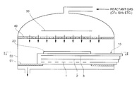
- FIG. 1 is a cross section schematically showing a configuration of a semiconductor manufacturing apparatus with a wafer holder in one embodiment of the present invention.
- FIG. 2 is a schematic cross section taken along the line II—II of FIG. 1 .
- FIG. 3 is a perspective view schematically showing a configuration of a wafer holder in one embodiment of the present invention.
- FIG. 4 is a plan view schematically showing a configuration of a wafer holder in one embodiment of the present invention.
- FIG. 5 is a schematic cross section taken along the line V—V of FIG. 4 .
- FIG. 6 is a plan view of an electrode for an electrostatic chuck as seen in the direction of the arrow VI of FIG. 5 .
- FIG. 7 is a plan view of the bottom electrode for generating a plasma, as seen in the direction of the arrow VII of FIG. 5 .
- FIG. 8 is a schematic plan view of a heater as seen in the direction of the arrow VIII of FIG. 5 .
- FIG. 9 is a plan view of a gap for insertion of a thermocouple as seen in the direction of the arrow IX of FIG. 5 .
- FIG. 10 is a cross section for illustrating another method of supporting a wafer holder.
- FIG. 11 is a schematic cross section showing a configuration of a wafer holder of a double-layered conductive layer.
- FIG. 12 is a schematic cross section showing a configuration of a wafer holder with a mono-layered conductive layer.
- FIG. 13 is a schematic cross section for illustrating a flush end surface of a side plate portion.
- FIG. 14 is a schematic cross section showing a configuration with a glass layer provided only between patterns.
- FIG. 15 is a plan view showing a configuration with a heater's heat emitting portion formed extending as far as a side plate portion.
- FIG. 16 is a perspective view for illustrating a wafer holder in the form of a polygon.
- FIG. 17 is a schematic cross section of another exemplary semiconductor manufacturing apparatus with a wafer holder in one embodiment of the present invention.
- FIG. 18 is a cross sectional view showing a protection layer covering a conductive layer.
- FIG. 19 is a schematic cross section showing a configuration of a conventional wafer holder.
- a semiconductor manufacturing apparatus is mainly formed for example of a vacuum chamber 50 having provided therein a wafer holder 10 , a top electrode 30 for generating a plasma, and a gas shower unit 40 .
- Wafer holder 10 is used to hold a wafer 20 and mainly has a heater 1 for heating wafer 20 , a bottom electrode 2 for generating a plasma, and an electrode 3 for an electrostatic chuck for holding wafer 20 .
- Wafer holder 10 sits and is thus held on a support 51 provided in the form e.g. of a doughnut provided on an inner wall surface of vacuum chamber 50 circumferentially.
- the semiconductor manufacturing apparatus is an etching apparatus, chemical vapor deposition (CVD) apparatus or a plasma CVD apparatus.
- CVD chemical vapor deposition
- Wafer holder 10 as shown in the FIG. 3 perspective view, has a generally round wafer holding portion and a side plate portion extending from a side surface of the wafer holding portion.
- the side plate portion has an end protruding outwardly of vacuum chamber 50 , as shown in FIGS. 1 and 2, for external, electrical connection.
- an O-ring 11 is arranged around the side plate portion to be between the side plate portion and vacuum chamber 50 .
- Wafer holder 10 is specifically configured as described hereinafter.
- wafer holder 10 is configured of a heater 1 , a bottom electrode 2 for generating a plasma and an electrode 3 for an electrostatic chuck that are each sandwiched by a ceramic base member 4 and thus stacked.
- Each ceramic base member 4 is bonded with a bonding layer 5 formed for example of an oxide layer such as a glass layer.
- the side plate portion has a stepwise end to allow heater 1 , the bottom electrode 2 for generating a plasma and the electrode 3 for an electrostatic chuck to have exposed pad portions 1 B, 2 B, 3 B.
- the exposed pad portions 1 B, 2 B, 3 B allow heater 1 and electrodes 2 and 3 to be externally, electrically connected.
- the ceramic base member 4 is also provided with a gap 4 A corresponding to a hole into which a thermocouple is externally inserted to measure the temperature of a surface of a wafer.
- the electrode 3 for an electrostatic chuck has a body 3 A formed across the substantially entire surface of the wafer holding portion, pad portion 3 B, and an extraction 3 C provided to connect body 3 A and pad portion 3 B together.
- Body 3 A, pad 3 B and extraction 3 C are provided substantially in a single plane.
- the bottom electrode 2 for generating a plasma has a body 2 A formed substantially over the entirety of the wafer holding portion, pad 2 B, and an extraction 2 C provided to connect body 2 A and pad 2 B together.
- Body 2 A, pad 2 B and extraction 2 C are provided substantially in a single plane.
- heater 1 has a body 1 A having a plurality of arcuate patterns on the wafer holding portion, pad 1 B, and an extraction 1 C provided to connect body 1 A and pad 1 B together.
- Body 1 A, pad 1 B and extraction 1 C are provided substantially in a single plane.
- heater 1 for example has five zones electrically divided. Each zone requires two pads 1 B and heater 1 thus has a total of ten pads 1 B, although heater 1 is not limited to a 5-zone heater.
- thermocouple As shown in FIG. 9, there are for example provided two gaps 4 A for insertion of a thermocouple to detect the temperature of a center of a wafer and that of a periphery of the wafer.
- the ceramic base member 4 is formed of a material resistant to heat and resistant to the corrosion attributed to a gaseous plasma containing halogen and it is preferably formed of at least one selected from the group consisting of aluminum nitride, silicon nitride, aluminum nitride oxide and aluminum oxide, more preferably aluminum nitride. Furthermore, the ceramic base member 4 preferably has a heat conductance of at least 100 W/mK.
- glass layer 5 serving as the bonding layer is preferably formed of a material containing at least one of glass having a thermal expansion coefficient of at least 3 ⁇ 10 ⁇ 6 /°C. and at most 8 ⁇ 10 ⁇ 6 /°C. and nonoxide ceramic having a thermal expansion coefficient of at least 3 ⁇ 10 ⁇ 6 /°C. and at most 6 ⁇ 10 ⁇ 6 /°C.
- nonoxide ceramic preferably contains at least 50% by mass of aluminum nitride or silicon nitride.
- bonding layer 5 is preferably formed of a material containing an oxide containing ytterbium, neodymium and calcium, or a compound producing an oxide containing ytterbium, neodymium and calcium when the compound is heated. If ceramic base member 4 is formed of silicon nitride, bonding layer 5 is preferably formed of a material containing an oxide containing yttrium and aluminum, or a compound producing an oxide containing yttrium and aluminum when the compound is heated.
- a width W 2 of the side plate portion is preferably smaller than a width W 1 of the wafer holding portion.
- At least bodies 1 A, 2 A, 3 A are preferably formed of at least one selected from the group consisting of W, Mo, Ag, Pd, Pt, Ni and Cr.
- wafer holder 10 preferably has a total thickness T of no more than 5 mm.
- heater 1 , the bottom electrode 2 for generating a plasma and the electrode 3 for an electrostatic chuck may each be a wire.
- the side plate portion is preferably provided with a neck 10 A corresponding for example to a groove, although neck 10 A is not limited to a groove and it may be formed by reducing the side plate portion in width.
- support 51 does not need to protrude in vacuum chamber 50 at the internal wall circumferentially and it may protrude partially, as shown in FIG. 10 .
- the conductive layer may have a double-layered structure formed of heater 1 and electrode 2 or 3 , as shown in FIG. 11 .
- one conductive layer may serve as both electrodes 2 and 3 .
- the conductive layer may have a mono-layered structure formed any one of heater 1 , the bottom electrode 2 for generating a plasma and the electrode 3 for an electrostatic chuck.
- the side plate portion may have an end formed stepwise, as shown in FIG. 5, alternatively it may be flush, as shown in FIG. 13 .
- the side plate portion has an end surface with heater 1 , the bottom electrode 2 for generating a plasma and the electrode 3 for an electrostatic chuck each exposed.
- bonding layer 5 is interposed between each of heater 1 , the bottom electrode 2 for generating a plasma and the electrode 3 for an electrostatic chuck, and ceramic base member 4 , bonding layer 5 may alternatively be provided only between patterns of a conductive layer such as heater 1 , as shown in FIG. 14 .
- heater 1 may have a heat emitting region corresponding to its body (the hatched region in the figure) 1 A that is provided not only in the wafer holding portion but also the side plate portion.
- the wafer holding portion is not limited to a round shape as seen in its plan view and it may be in the form of a polygon (for example a quadrangle), as shown in FIG. 16 .
- wafer holder 10 of the present embodiment may also be applied to a semiconductor manufacturing apparatus which does not have an electrode for generating a plasma, as shown in FIG. 17 . In this configuration, wafer holder 10 does not require a bottom electrode for generating a plasma.
- the wafer holder is manufactured in the method as will now be described hereinafter.
- Ceramic base member 4 can be prepared by a conventional method, adding a sintering assistant to powdery ceramic, as required, and furthermore adding a binder thereto, as required, and molding and sintering the same. Ceramic base member 4 is preferably formed for example of aluminum nitride as it is highly resistant to heat and highly resistant to the corrosion attributed to a gaseous plasma containing halogen, as has been previously described.
- the sintered compact may be hot-pressed and thus densified, since, as has been described above, it should be resistant to corrosion and it is thus desirable that it contain as small an amount of a secondary component other than the aforementioned main component as possible.
- the molded and dried medium is blanked or cut in a shape allowing for its degree of contraction when it is sintered. It has a shape of a disk (or an angular plate) with an angular plate (a side plate) joined to a side of the disk or angular plate, as shown in FIG. 3 .
- the disk portion corresponds to the portion on which a wafer is placed and heated, and the side plate portion protects an extraction line supplying power to heater 1 and electrodes 2 and 3 against fluoride gas, chloride gas and the like.
- the medium is sintered. While desirably the medium is sintered pressurelessly, it may be sintered otherwise.
- the sintered compact may be polished, cut or the like, as required, or it may be used as it is if its size, warpage and the like fall within a predetermined range.
- an electrode corresponding to the bottom electrode 2 for generating a plasma and that corresponding to the electrode 3 for an electrostatic chuck are formed by applying a paste containing a refractory metal such as W, Mo and the like or a mixture thereof or a heat-emission resistance substance such as Ag, Ag—Pd, Ni—Cr and the like, and removing a binder from a volatile component in the paste and then firing the sintered compact thus prepared.
- a paste containing a refractory metal such as W, Mo and the like or a mixture thereof or a heat-emission resistance substance such as Ag, Ag—Pd, Ni—Cr and the like
- heater 1 and electrodes corresponding to electrodes 2 and 3 may be formed on a sheet by printing a refractory metal such as W, Mo and the like or a mixture thereof and removing a binder therefrom and then sintering the aluminum nitride and firing the refractory metal simultaneously, i.e., co-firing them.
- a refractory metal such as W, Mo and the like or a mixture thereof
- the above-described metalized substrates or a metalized substrate and a non-metalized substrate after a bonding component is applied thereto are placed one on the other and thus bonded together. If they are used to provide a heater layer then they may be bonded together with a wire of such pyrogenic substances sandwiched therebetween. In such configuration, the heater layer desirably has as small a thickness as possible.
- the adhesive component used to bond the substrates together may be determined depending on the environment in which the product is used, such as temperature, ambient gas and the like. If the product is used at relatively low temperatures the substrates may be bonded together with an organic adhesive. If the product is used at high temperatures then the substrates are preferably bonded together with an inorganic glass or nonoxide ceramic having a heat resistance higher than the temperature of interest. To reduce the thermal stress after the substrates are bonded together, the glass preferably has a thermal expansion coefficient substantially equal to that of ceramic base member 4 . For example, if ceramic base member 4 contains aluminum nitride or silicon nitride as a main component thereof, it desirably has a thermal expansion coefficient of at least 3.0 ⁇ 10 ⁇ 6 /°C.
- either one of stacked ceramic base members 4 can have its side plate portion one side simply reduced in length. Providing a pad at an end of the interconnection facilitate bonding the interconnection.
- heater 1 has body 1 A (the hatched region) reaching a portion of the side plate portion to allow the wafer holding portion to have uniform heat, and at a portion closer to the end than body 1 A a groove 10 A is provided as shown in FIG. 4 or the width is reduced to minimize heat dissipation.
- heater 1 bottom electrode 2 and the electrode 3 for an electrostatic chuck corresponding to conductive layers are each sandwiched between a pair of ceramic base members 4
- conductive layers 1 , 2 , 3 are not required to be sandwiched between ceramic base members 4 and as shown in FIG. 18 they may be formed on ceramic base member 4 and covered by a protection layer 6 .
- the conductive layer 1 , 2 , 3 , body 1 A, 2 A, 3 A and extraction 1 C, 2 C, 3 C are provided in a single plane.
- the coverage with protection layer 6 can protect conductive layers 1 , 2 , 3 .
- This also eliminates the necessity of providing the step of bonding the pipe and thus facilitates the fabrication and also prevents such distortion as caused in providing such pipe.
- Protection layer 6 is preferably formed of a material containing at least one of glass having a thermal expansion coefficient of at least 3 ⁇ 10 ⁇ 6 /°C. and at most 8 ⁇ 10 ⁇ 6 /°C. and nonoxide ceramic having a thermal expansion coefficient of at least 3 ⁇ 10 31 6 /°C. and at most 6 ⁇ 10 ⁇ 6 /°C. Furthermore, the nonoxide ceramic is preferably formed of a material containing 50% by mass of aluminum nitride or silicon nitride.
- protection layer 6 is preferably formed of a material containing an oxide containing ytterbium, neodymium and calcium or a compound producing an oxide containing ytterbium, neodymium and calcium when it is heated. Furthermore, if ceramic base member 4 is formed of silicon nitride, protection layer 6 is preferably formed of a material containing an oxide containing yttrium and aluminum or a compound producing an oxide containing yttrium and aluminum when it is heated.
- ceramic base member 4 may have therein groove 4 a corresponding to a hole for insertion of a temperature detection unit. Furthermore, ceramic base member 4 and protection layer 6 may each have a wafer holding portion sandwiching the body and a side plate portion extending from a side surface of the wafer holding portion and sandwiching the extraction, as shown in FIG. 18, and the side plate portion may have a width smaller than that of the wafer holding portion, as shown in FIG. 3 .
- FIG. 3 there may be an O ring 11 arranged at those side plate portions of ceramic base member 4 and protection layer 6 sandwiching the extraction.
- FIG. 18 there may also be a heat insulating recess 10 A provided at the side plate portion of at least one of ceramic base member 4 and protection layer 6 sandwiching the extraction.
- FIG. 15 there may also be provided the heater 1 body at that region of the side plate portion sandwiched between ceramic base member 4 and protection layer 6 .
- a total thickness T 1 is preferably no more than 5 mm.
- conductive layers 1 , 2 , 3 preferably at least have their respective bodies formed of at least one element selected from the group consisting of W, Mo, Ag, Pd, Pt, Ni and Cr. Furthermore, conductive layers 1 , 2 , 3 may be wire.
- Powdery aluminum nitride with 5% by mass of Y 2 O 3 as a sintering assistant and a binder added thereto were dispersedly mixed and then doctor-blade molded so that it has a thickness of 1.0 mm when it has been sintered. After the molded medium is dried, it was blanked to provide two piece of the medium each in the form of a table-tennis racket (as shown in FIG. 3) having a disk portion (a wafer holding portion) of ⁇ 300 mm and a side plate portion of 50 mm in width and 100 mm in length when it has been sintered.
- the sintered compacts had their upper and lower surfaces polished with diamond abrasive grains.
- the sintered compact of aluminum nitride had a heat conductance of 175 W/mK and a thermal expansion coefficient of 4.5 ⁇ 10 ⁇ 6 /°C.
- Powdery W and a sintering assistant were kneaded with a binder and then printed on one substrate. It was printed in a line of a W line width of 0.5 mm and a line spacing of 0.5 mm.
- the pattern was designed spirally provided on the disk portion and passed through the side plate portion and bonded to an external electrode. It was then degreased in nitrogen at 800° C. and baked in nitrogen at 1600° C. Furthermore, the other sintered compact was printed with powdery glass having a thermal expansion coefficient of 5.0 ⁇ 10 ⁇ 6/°C. It was then degreased at 500° C. and then stacked on the sintered compact provided with the electrode. The sintered compacts stacked were then fastened with a jig made of Mo plus a weight thereon and they were thus bonded together in nitrogen at 650° C.
- the wafer holder thus obtained had a configuration, a heat uniformity, a temperature drop rate, an anti-corrosion property and a heat cycle (H/C), as presented in Table 1.
- Table 1 also presents the results of examples 2-15 described hereinafter.
- a voltage of 200V was applied to pass current to heat a surface of the disk to 700° C.
- the disk portion corresponding to the wafer portion had a temperature distribution of ⁇ 0.5° C. It was also exposed to fluorine gas at 700° C. for 1000 hours and it did not corrode.
- Powdery W and a sintering assistant were kneaded with a binder and printed on one molded medium.
- the printed pattern is a linear pattern having a W line width of 0.5 mm and a line spacing of 0.5 mm when the molded medium has been sintered. It was designed to be spirally provided on the disk portion and passed through the side plate portion and bonded to an external electrode. Thereon the other molded medium was placed and they were thermally contact-bonded together. They were degreased in a stream of gaseous nitrogen at 800° C. and simultaneously sintered at 1800° C. for four hours. The obtained sintered compact had a heat conductance of 175 W/mK.
- a voltage of 200V was applied to pass current to heat a surface of the disk to 700° C.
- the disk portion corresponding to the wafer portion had a temperature distribution of ⁇ 1.0° C. It was also exposed to fluorine gas at 700° C. for 1000 hours and it did not corrode.
- Powdery Ag—Pd and a sintering assistant were kneaded with a binder and printed on a single substrate.
- the printed pattern was a linear pattern having a W line width of 0.5 mm and a line spacing of 0.5 mm. It was designed to be spirally provided on the disk portion and passed through the side plate portion and bonded to an external electrode. It was degreased in the air at 500° C. and baked in nitrogen at 800° C. Furthermore the other sintered compact was printed thereon with powdery glass having a thermal expansion coefficient of 5.0 ⁇ 10 ⁇ 6 /°C. It was then degreased at 500° C. and then placed on the sintered compact provided with the electrode. They were then fastened by a jig made of Mo and had a weight placed thereon and were thus bonded together in nitrogen at 650° C.
- a voltage of 200V was applied to pass current to heat a surface of the disk to 700° C.
- the disk portion corresponding to the wafer portion had a temperature distribution of ⁇ 1.5° C. It was also exposed to fluorine gas at 700° C. for 1000 hours and it did not corrode.
- the same method as employed in the first example was employed to prepare a bonded body, except that the bonding glass used had a different thermal expansion coefficient of 2.0 ⁇ 10 ⁇ 6 /°C.
- a voltage of 200V was applied to pass current to heat a surface of the disk to 700° C.
- the disk portion corresponding to the wafer portion had a temperature distribution of ⁇ 0.7° C. It was also exposed to fluorine gas at 700° C. for 1000 hours and it did not corrode.
- the same method as employed in the first example was employed to prepare a bonded body, except that the bonding glass used had a different thermal expansion coefficient of 9.0 ⁇ 10 ⁇ 6 /°C.
- a voltage of 200V was applied to pass current to heat a surface of the disk to 700° C.
- the disk portion corresponding to the wafer portion had a temperature distribution of ⁇ 0.5° C. It was also exposed to fluorine gas at 700° C. for 1000 hours and it did not corrode.
- the same method as employed in the first example was employed to prepare one W metalized substrate and five non-metalized substrates.
- the substrates were stacked, three non-metalized substrates placed upward of the W metalized substrate and two non-metalized substrates placed downward of the W metalized substrate, and they were bonded together by the same technique as employed in the first example.
- a voltage of 200V was applied to pass current to heat a surface of the disk to 7000° C.
- the disk portion corresponding to the wafer portion had a temperature distribution of ⁇ 0.6° C. It was also exposed to fluorine gas at 7000° C. for 1000 hours and it did not corrode.
- the two pieces of the medium were degreased in a stream of gaseous nitrogen at 800° C.
- the obtained sintered compacts had their upper and lower surfaces polished with diamond abrasive.
- the obtained sintered compacts had a heat conductance of 30 W/mK and a thermal expansion coefficient of 3.0 ⁇ 10 ⁇ 6 /°C.
- Powdery W and a sintering assistant were kneaded with a binder and printed on a single substrate.
- the printed pattern was a linear pattern having a W line width of 0.5 mm and a line spacing of 0.5 mm. It was designed to be spirally provided on the disk portion and passed through the side plate portion and bonded to an external electrode. It was degreased in the air at 800° C. and baked in nitrogen at 1600° C. Furthermore the other sintered compact was printed thereon with powdery glass having a thermal expansion coefficient of 5.0 ⁇ 10 ⁇ 6 /°C. It was then degreased at 500° C. and then placed on the sintered compact provided with the electrode. They were then fastened by a jig made of Mo and had a weight placed thereon and were thus bonded together in nitrogen at 650° C.
- a voltage of 200V was applied to pass current to heat a surface of the disk to 700° C.
- the disk portion corresponding to the wafer portion had a temperature distribution of ⁇ 4.0° C. It was also exposed to fluorine gas at 700° C. for 1000 hours and it did not corrode.
- the two pieces of the medium were degreased in a stream of gaseous nitrogen at 800° C. and sintered at 1770° C. for four hours.
- the obtained sintered compacts had their upper and lower surfaces polished with diamond abrasive.
- the obtained sintered compacts had a heat conductance of 50 W/mK and a thermal expansion coefficient of 5.0 ⁇ 10 ⁇ 6 /
- Powdery W and a sintering assistant were kneaded with a binder and printed on a single substrate.
- the printed pattern was a linear pattern having a W line width of 0.5 mm and a line spacing of 0.5 mm. It was designed to be spirally provided on the disk portion and passed through the side plate portion and bonded to an external electrode. It was degreased in the air at 800° C. and baked in nitrogen at 1600° C. Furthermore the other sintered compact was printed thereon with powdery glass having a thermal expansion coefficient of 5.0 ⁇ 10 ⁇ 6 /°C. It was then degreased at 500° C. and then placed on the sintered compact provided with the electrode. They were then fastened by a jig made of Mo and had a weight placed thereon and were thus bonded together in nitrogen at 650° C.
- a voltage of 200V was applied to pass current to heat a surface of the disk to 700° C.
- the disk portion corresponding to the wafer portion had a temperature distribution of ⁇ 5.0° C. It was also exposed to fluorine gas at 700° C. for 1000 hours and it did not corrode.
- the two pieces of the medium were degreased in a stream of gaseous nitrogen at 800° C. and sintered at 1450° C. for four hours.
- the obtained sintered compacts had their upper and lower surfaces polished with diamond abrasive.
- the obtained sintered compacts had a heat conductance of 10 W/mK and a thermal expansion coefficient of 8.5 ⁇ 10 ⁇
- Powdery W and a sintering assistant were kneaded with a binder and printed on a single substrate.
- the printed pattern was a linear pattern having a W line width of 0.5 mm and a line spacing of 0.5 mm. It was designed to be spirally provided on the disk portion and passed through the side plate portion and bonded to an external electrode. It was degreased in nitrogen at 800° C. and baked in nitrogen at 1600° C. Furthermore the other sintered compact was printed thereon with powdery glass having a thermal expansion coefficient of 5.0 ⁇ 10 ⁇ 6 /°C. It was then degreased at 500° C. and then placed on the sintered compact provided with the electrode. They were then fastened by a jig made of Mo and had a weight placed thereon and were thus bonded together in nitrogen at 650° C.
- the disk portion corresponding to the wafer portion had a temperature distribution of ⁇ 7.0° C.
- One molded medium had Mo of 0.5 mm ⁇ and having a coil winding diameter of 1.0 mm ⁇ and buried in and thus spirally running along its groove and thereon the other molded medium is placed and they were thus hot-pressed and thus sintered at 1850° C. to provide a sintered compact having a thickness of 4 mm.
- the sintered compact had a heat conductance of 173 W/mK and a thermal expansion coefficient of 4.5 ⁇ 10 ⁇ 6 /°C.
- a voltage of 200V was applied to pass current to heat a surface of the disk to 700° C.
- the disk portion corresponding to the wafer portion had a temperature distribution of ⁇ 9.0° C. It was also exposed to fluorine gas at 7000° C. for 1000 hours and it did not corrode.
- the same method as employed in the first example was employed to prepare one W metalized substrate and one non-metalized substrate. With the W metalized substrate interposed, the non-metalized substrate is stacked, and a layer of AIN with Y—Ca—O added thereto by 3% was applied thereto and the substrates were stacked together and thus sintered in N 2 at 1600° C. and thus bonded together.
- the metalization had its back surface regarded as a wafer holding surface and heated and the wafer holding surface had a temperature of 700° C. ⁇ 2.0° C. It was also exposed to fluorine gas at 750° C. for 1000 hours and it did not corrode.
- the same method as employed in the first example was employed to prepare a single W metalized substrate.
- a paste of AlN with Yb—Nd—Ca—O added thereto by 3% was applied to the substrate and thus sintered in N 2 at 1600° C. to provide a protection layer.
- the metalization had its back surface regarded as a wafer holding surface and heated and the wafer holding surface had a temperature of 700° C. ⁇ 2.5° C. It was also exposed to fluorine gas at 750° C. for 1000 hours and it did not corrode.
- the same method as employed in the first example was employed to prepare two sintered compacts.
- the same conditions as applied in the first example were applied to prepare a wafer holder, except that on one sintered compact a paste of Mo was applied in a linear pattern having a width of 0.5 mm and a spacing of 0.5 mm and it was thus baked in nitrogen (N 2 ) to provide a conductive layer.
- N 2 nitrogen
- a wafer On the wafer holder a wafer had its surface temperature distribution measured under the same conditions as in the first example and it had a temperature of 700° C. ⁇ 3° C. Furthermore it was exposed to fluorine gas at 700° C. for 1000 hours and it did not corrode.
- the same method as employed in the first example was employed to prepare two sintered compacts.
- the same conditions as applied in the first example were applied to prepare a wafer holder, except that on one sintered compact a paste of Ag—Pd was applied in a linear pattern having a width of 0.5 mm and a spacing of 0.5 mm and it was thus baked in nitrogen (N 2 ) to provide a conductive layer.
- N 2 nitrogen
- a wafer had its surface temperature distribution measured under the same conditions as in the first example and it had a temperature of 700° C. ⁇ 5° C. Furthermore it was exposed to fluorine gas at 700° C. for 1000 hours and it did not corrode.
- the same method as employed in the first example was employed to prepare two sintered compacts.
- the same conditions as applied in the first example were applied to prepare a wafer holder, except that on one sintered compact a paste of Ni—Cr was applied in a linear pattern having a width of 0.5 mm and a spacing of 0.5 mm and it was thus baked in nitrogen (N 2 ) to provide a conductive layer.
- N 2 nitrogen
- a wafer had its surface temperature distribution measured under the same conditions as in the first example and it had a temperature of 700° C. ⁇ 4° C. Furthermore it was exposed to fluorine gas at 700° C. for 1000 hours and it did not corrode.
- Each molded medium was provided thereon with Mo of 0.5 mm ⁇ having a coil winding diameter of 5 mm ⁇ spirally with a pitch of 10 mm and it was thus hot-pressed and thus sintered at 1850° C.
- the sintered compact obtained had a heat conductance of 173 W/mK and a thermal expansion coefficient of 4.5 ⁇ 10 ⁇ 6 /°C.
- a pipe of aluminum nitride of 80 mm ⁇ having a thickness of 5 mm was diffusingly bonded on a back side of the disk.
- a wire made of Mo was passed through the pipe and silver-soldered to an electrode terminal of a Mo coil.
- a voltage of 200V was applied to pass current to heat a surface of the disk to 700° C.
- the disk portion corresponding to the wafer portion had a temperature distribution of ⁇ 12.0° C. It was also exposed to fluorine gas at 750° C. for 1000 hours and it did not corrode.
- Table 3 presents the configuration, heat uniformity, temperature reduction rate, anti-corrosion property and heat cycle (H/C) of the obtained wafer holder. Table 3 also presents those of second and third comparative examples described hereinafter.
- the two pieces of the medium were degreased in a stream of gaseous nitrogen at 800° C. and sintered at 1800° C. for four hours.
- the obtained sintered compacts had their upper and lower surfaces polished with diamond abrasive.
- the obtained sintered compacts had a heat conductance of 175 W/mK and a thermal expansion coefficient of 4.5 ⁇ 10 ⁇ 6 /°C.
- Powdery W and a sintering assistant were kneaded with a binder and printed on a single substrate.
- the printed pattern was a linear pattern having a W line width of 0.6 mm and a line spacing of 0.5 mm. It was spirally provided on the disk portion and patterned to allow an electrode terminal to be positioned at the center on the back side.
- Glass having a thermal expansion coefficient of 5.0 ⁇ 10 ⁇ 6 /°C. was used to bond a pipe of 80 mm ⁇ having a thickness of 5 mm to a back side of the disk.
- a wire made of Mo was passed through the pipe and silver-soldered to an electrode terminal of the W metalization.
- a voltage of 200V was applied to pass current to heat a surface of the disk to 700° C.
- the disk portion corresponding to the wafer portion had a temperature distribution of ⁇ 10.0° C. It was also exposed to fluorine gas at 700° C. for 1000 hours and it did not corrode.
- a pipe made of SUS310 of 80 mm ⁇ having a thickness of 5 mm was silver-soldered and thus bonded to a back side of a disk and simultaneously a wire made of Mo was passed through the pipe and silver-soldered to an electrode terminal of the W metalization.
- a voltage of 200V was applied to pass current to heat a surface of the disk to 700° C.
- the disk portion corresponding to the wafer portion had a temperature distribution of ⁇ 10.0° C. It was also exposed to fluorine gas at 700° C. for 1000 hours and it did not corrode.
- the disk of aluminum nitride and the pipe's bonded portion cracked when the wafer holder was cooled as described above only once.
- the present invention in one and another aspect provides a wafer holder for a semiconductor manufacturing apparatus that has a conductive layer having a body and an extraction substantially provided in a single plane to allow the body and the extraction to be sandwiched by paired ceramic base members and thus protected or to be covered by a protection layer to protect the conductive layer.
- a conductive layer having a body and an extraction substantially provided in a single plane to allow the body and the extraction to be sandwiched by paired ceramic base members and thus protected or to be covered by a protection layer to protect the conductive layer.
- This can eliminate the necessity of using a pipe to protect the extraction, as conventional.
- the step of bonding the pipe can be dispensed with to facilitate producing the wafer holder and also allow the wafer holder to be free of such distortion as attributed to installing the pipe.
- a wafer holder of a semiconductor manufacturing apparatus for etching, deposition and the like that is increased in diameter and required to uniformly heat a wafer
- a product also functioning as both a heater and an electrostatic chuck as well as achieving high heat uniformity, having less warpage and being inexpensive and significantly suitable for mass-production.
Landscapes
- Container, Conveyance, Adherence, Positioning, Of Wafer (AREA)
- Drying Of Semiconductors (AREA)
Applications Claiming Priority (4)
| Application Number | Priority Date | Filing Date | Title |
|---|---|---|---|
| JP2000012170 | 2000-01-20 | ||
| JP2000-012170 | 2000-01-20 | ||
| JP2000-160366 | 2000-05-30 | ||
| JP2000160366A JP3567855B2 (ja) | 2000-01-20 | 2000-05-30 | 半導体製造装置用ウェハ保持体 |
Publications (1)
| Publication Number | Publication Date |
|---|---|
| US6554906B1 true US6554906B1 (en) | 2003-04-29 |
Family
ID=26583878
Family Applications (1)
| Application Number | Title | Priority Date | Filing Date |
|---|---|---|---|
| US09/707,813 Expired - Fee Related US6554906B1 (en) | 2000-01-20 | 2000-11-07 | Wafer holder for semiconductor manufacturing apparatus and semiconductor manufacturing apparatus using the same |
Country Status (6)
| Country | Link |
|---|---|
| US (1) | US6554906B1 (fr) |
| EP (1) | EP1119026A3 (fr) |
| JP (1) | JP3567855B2 (fr) |
| KR (1) | KR100438881B1 (fr) |
| CA (1) | CA2326575C (fr) |
| TW (1) | TW557531B (fr) |
Cited By (27)
| Publication number | Priority date | Publication date | Assignee | Title |
|---|---|---|---|---|
| US20030029569A1 (en) * | 2001-04-11 | 2003-02-13 | Sumitomo Electric Industries, Ltd. | Substrate processing apparatus |
| US20040060656A1 (en) * | 2002-09-30 | 2004-04-01 | Tokyo Electron Limited | Method and apparatus for an improved bellows shield in a plasma processing system |
| US20040063333A1 (en) * | 2002-09-30 | 2004-04-01 | Tokyo Electron Limited | Method and apparatus for an improved baffle plate in a plasma processing system |
| US20040061447A1 (en) * | 2002-09-30 | 2004-04-01 | Tokyo Electron Limited | Method and apparatus for an improved upper electrode plate in a plasma processing system |
| US20040060661A1 (en) * | 2002-09-30 | 2004-04-01 | Tokyo Electron Limited | Method and apparatus for an improved upper electrode plate with deposition shield in a plasma processing system |
| US20040060657A1 (en) * | 2002-09-30 | 2004-04-01 | Tokyo Electron Limited | Method and apparatus for an improved deposition shield in a plasma processing system |
| US6716304B2 (en) * | 2000-01-20 | 2004-04-06 | Sumitomo Electric Industries, Ltd. | Wafer holder for semiconductor manufacturing apparatus, and method of manufacturing the wafer holder |
| US20040144492A1 (en) * | 2001-06-01 | 2004-07-29 | Taro Ikeda | Plasma processing device |
| US20040173155A1 (en) * | 2002-09-30 | 2004-09-09 | Tokyo Electron Limited | Method and apparatus for an improved optical window deposition shield in a plasma processing system |
| US20040216667A1 (en) * | 2002-11-28 | 2004-11-04 | Tokyo Electron Limited | Internal member of a plasma processing vessel |
| US20050101113A1 (en) * | 2003-11-06 | 2005-05-12 | Brask Justin K. | Method for making a semiconductor device having a metal gate electrode |
| US20050103268A1 (en) * | 2002-09-30 | 2005-05-19 | Tokyo Electron Limited | Method and apparatus for an improved baffle plate in a plasma processing system |
| US20050121417A1 (en) * | 1994-08-12 | 2005-06-09 | Diamicron, Inc. | Brut polishing of superhard materials |
| US7048488B1 (en) * | 1999-05-07 | 2006-05-23 | Asm International N.V. | Apparatus for transferring wafer and ring |
| US20060118045A1 (en) * | 2004-12-08 | 2006-06-08 | Fink Steven T | Method and apparatus for improved baffle plate |
| US20060151114A1 (en) * | 2005-01-11 | 2006-07-13 | Fink Steven T | Plasma processing system and baffle assembly for use in plasma processing system |
| US20060183344A1 (en) * | 2003-03-31 | 2006-08-17 | Tokyo Electron Limited | Barrier layer for a processing element and a method of forming the same |
| US20060225654A1 (en) * | 2005-03-29 | 2006-10-12 | Fink Steven T | Disposable plasma reactor materials and methods |
| US20060254716A1 (en) * | 2004-07-06 | 2006-11-16 | Tokyo Electron Limited | Processing system and method for chemically treating a tera layer |
| US20080069966A1 (en) * | 1999-12-10 | 2008-03-20 | Tokyo Electron Limited | Processing apparatus with a chamber having therein a high-corrosion-resistant sprayed film |
| US7560376B2 (en) | 2003-03-31 | 2009-07-14 | Tokyo Electron Limited | Method for adjoining adjacent coatings on a processing element |
| US20100103584A1 (en) * | 2008-10-28 | 2010-04-29 | Jusung Engineering Co., Ltd. | Electrostatic chucking apparatus and method for manufacturing the same |
| US20110139399A1 (en) * | 2009-12-15 | 2011-06-16 | Sumitomo Electric Industries, Ltd. | Heater unit, heating and cooling device, and apparatus comprising same |
| US20120285619A1 (en) * | 2006-04-27 | 2012-11-15 | Alexander Matyushkin | Electrostatic chuck having a plurality of heater coils |
| US9196516B2 (en) | 2013-03-14 | 2015-11-24 | Qualitau, Inc. | Wafer temperature measurement tool |
| US20170140958A1 (en) * | 2014-05-19 | 2017-05-18 | Tokyo Electron Limited | Heater power feeding mechanism |
| US20210125853A1 (en) * | 2019-10-24 | 2021-04-29 | Asm Ip Holding B.V. | Susceptor for semiconductor substrate processing |
Families Citing this family (7)
| Publication number | Priority date | Publication date | Assignee | Title |
|---|---|---|---|---|
| WO2006046308A1 (fr) * | 2004-10-29 | 2006-05-04 | Cxe Japan Co., Ltd. | Support pour substrat semi-conducteur |
| KR101342990B1 (ko) * | 2007-03-08 | 2013-12-18 | (주)소슬 | 배치식 기판 처리 장치 및 이를 이용하는 기판 처리 방법 |
| US12567564B2 (en) | 2015-11-16 | 2026-03-03 | Coorstek, Inc. | Corrosion-resistant components |
| EP3377318A1 (fr) | 2015-11-16 | 2018-09-26 | Coorstek Inc. | Composants résistant à la corrosion et procédés de réalisation |
| CN109963825B (zh) * | 2016-11-16 | 2022-08-09 | 阔斯泰公司 | 耐腐蚀组件和制造方法 |
| CN113066755B (zh) * | 2021-03-23 | 2023-06-13 | 西安微电子技术研究所 | 一种芯片背面金属化夹具及芯片背面金属化方法 |
| CN114776926A (zh) * | 2022-03-09 | 2022-07-22 | 青海丽豪半导体材料有限公司 | 一种高温氯气加热的方法 |
Citations (7)
| Publication number | Priority date | Publication date | Assignee | Title |
|---|---|---|---|---|
| WO1995030031A1 (fr) | 1994-05-03 | 1995-11-09 | Applied Materials, Inc. | Suscepteur soude |
| US5855687A (en) * | 1990-12-05 | 1999-01-05 | Applied Materials, Inc. | Substrate support shield in wafer processing reactors |
| US5904872A (en) * | 1994-09-29 | 1999-05-18 | Tokyo Electron Limited | Heating device, method of manufacturing the same, and processing apparatus using the same |
| US5997651A (en) * | 1995-10-18 | 1999-12-07 | Tokyo Electron Limited | Heat treatment apparatus |
| US6080969A (en) * | 1997-05-29 | 2000-06-27 | Smc Corporation | Apparatus for and method of thermally processing substrate |
| US6204489B1 (en) * | 1998-01-09 | 2001-03-20 | Ngk Insulators, Ltd. | Electrically heated substrate with multiple ceramic parts each having different volume restivities |
| US6423949B1 (en) * | 1999-05-19 | 2002-07-23 | Applied Materials, Inc. | Multi-zone resistive heater |
Family Cites Families (6)
| Publication number | Priority date | Publication date | Assignee | Title |
|---|---|---|---|---|
| JPH06120328A (ja) * | 1992-10-02 | 1994-04-28 | Hitachi Chem Co Ltd | 静電ウエーハチャック用プレート |
| KR100238627B1 (ko) * | 1993-01-12 | 2000-01-15 | 히가시 데쓰로 | 플라즈마 처리장치 |
| US5708556A (en) * | 1995-07-10 | 1998-01-13 | Watkins Johnson Company | Electrostatic chuck assembly |
| JPH09172057A (ja) * | 1995-12-20 | 1997-06-30 | Souzou Kagaku:Kk | 静電チャック |
| JPH113868A (ja) * | 1997-06-12 | 1999-01-06 | Nec Yamagata Ltd | ランプアニール装置およびランプアニール方法 |
| US6019164A (en) * | 1997-12-31 | 2000-02-01 | Temptronic Corporation | Workpiece chuck |
-
2000
- 2000-05-30 JP JP2000160366A patent/JP3567855B2/ja not_active Expired - Fee Related
- 2000-11-07 US US09/707,813 patent/US6554906B1/en not_active Expired - Fee Related
- 2000-11-16 CA CA002326575A patent/CA2326575C/fr not_active Expired - Fee Related
-
2001
- 2001-01-16 TW TW090100935A patent/TW557531B/zh not_active IP Right Cessation
- 2001-01-19 KR KR10-2001-0003125A patent/KR100438881B1/ko not_active Expired - Fee Related
- 2001-01-19 EP EP01300468A patent/EP1119026A3/fr not_active Withdrawn
Patent Citations (8)
| Publication number | Priority date | Publication date | Assignee | Title |
|---|---|---|---|---|
| US5855687A (en) * | 1990-12-05 | 1999-01-05 | Applied Materials, Inc. | Substrate support shield in wafer processing reactors |
| WO1995030031A1 (fr) | 1994-05-03 | 1995-11-09 | Applied Materials, Inc. | Suscepteur soude |
| JPH09503349A (ja) | 1994-05-03 | 1997-03-31 | アプライド マテリアルズ インコーポレイテッド | 溶着されたサセプタ組立体 |
| US5904872A (en) * | 1994-09-29 | 1999-05-18 | Tokyo Electron Limited | Heating device, method of manufacturing the same, and processing apparatus using the same |
| US5997651A (en) * | 1995-10-18 | 1999-12-07 | Tokyo Electron Limited | Heat treatment apparatus |
| US6080969A (en) * | 1997-05-29 | 2000-06-27 | Smc Corporation | Apparatus for and method of thermally processing substrate |
| US6204489B1 (en) * | 1998-01-09 | 2001-03-20 | Ngk Insulators, Ltd. | Electrically heated substrate with multiple ceramic parts each having different volume restivities |
| US6423949B1 (en) * | 1999-05-19 | 2002-07-23 | Applied Materials, Inc. | Multi-zone resistive heater |
Cited By (64)
| Publication number | Priority date | Publication date | Assignee | Title |
|---|---|---|---|---|
| US20050121417A1 (en) * | 1994-08-12 | 2005-06-09 | Diamicron, Inc. | Brut polishing of superhard materials |
| US7465219B2 (en) * | 1994-08-12 | 2008-12-16 | Diamicron, Inc. | Brut polishing of superhard materials |
| US7048488B1 (en) * | 1999-05-07 | 2006-05-23 | Asm International N.V. | Apparatus for transferring wafer and ring |
| US7879179B2 (en) | 1999-12-10 | 2011-02-01 | Tokyo Electron Limited | Processing apparatus with a chamber having therein a high-corrosion-resistant sprayed film |
| US7846291B2 (en) | 1999-12-10 | 2010-12-07 | Tokyo Electron Limited | Processing apparatus with a chamber having therein a high-corrosion-resistant sprayed film |
| US20080070032A1 (en) * | 1999-12-10 | 2008-03-20 | Tokyo Electron Limited | Processing apparatus with a chamber having therein a high-corrosion-resistant sprayed film |
| US20080069966A1 (en) * | 1999-12-10 | 2008-03-20 | Tokyo Electron Limited | Processing apparatus with a chamber having therein a high-corrosion-resistant sprayed film |
| US6716304B2 (en) * | 2000-01-20 | 2004-04-06 | Sumitomo Electric Industries, Ltd. | Wafer holder for semiconductor manufacturing apparatus, and method of manufacturing the wafer holder |
| US7361230B2 (en) * | 2001-04-11 | 2008-04-22 | Sumitomo Electric Industries, Ltd. | Substrate processing apparatus |
| US20030029569A1 (en) * | 2001-04-11 | 2003-02-13 | Sumitomo Electric Industries, Ltd. | Substrate processing apparatus |
| US20090314435A1 (en) * | 2001-06-01 | 2009-12-24 | Tokyo Electron Limited | Plasma processing unit |
| US20040144492A1 (en) * | 2001-06-01 | 2004-07-29 | Taro Ikeda | Plasma processing device |
| US7282112B2 (en) | 2002-09-30 | 2007-10-16 | Tokyo Electron Limited | Method and apparatus for an improved baffle plate in a plasma processing system |
| US20070034337A1 (en) * | 2002-09-30 | 2007-02-15 | Tokyo Electron Limited | Method and apparatus for an improved upper electrode plate with deposition shield in a plasma processing system |
| US8118936B2 (en) | 2002-09-30 | 2012-02-21 | Tokyo Electron Limited | Method and apparatus for an improved baffle plate in a plasma processing system |
| US8117986B2 (en) | 2002-09-30 | 2012-02-21 | Tokyo Electron Limited | Apparatus for an improved deposition shield in a plasma processing system |
| US8057600B2 (en) | 2002-09-30 | 2011-11-15 | Tokyo Electron Limited | Method and apparatus for an improved baffle plate in a plasma processing system |
| US20040060656A1 (en) * | 2002-09-30 | 2004-04-01 | Tokyo Electron Limited | Method and apparatus for an improved bellows shield in a plasma processing system |
| US20050103268A1 (en) * | 2002-09-30 | 2005-05-19 | Tokyo Electron Limited | Method and apparatus for an improved baffle plate in a plasma processing system |
| US7137353B2 (en) | 2002-09-30 | 2006-11-21 | Tokyo Electron Limited | Method and apparatus for an improved deposition shield in a plasma processing system |
| US7147749B2 (en) | 2002-09-30 | 2006-12-12 | Tokyo Electron Limited | Method and apparatus for an improved upper electrode plate with deposition shield in a plasma processing system |
| US7163585B2 (en) | 2002-09-30 | 2007-01-16 | Tokyo Electron Limited | Method and apparatus for an improved optical window deposition shield in a plasma processing system |
| US7166200B2 (en) | 2002-09-30 | 2007-01-23 | Tokyo Electron Limited | Method and apparatus for an improved upper electrode plate in a plasma processing system |
| US7166166B2 (en) * | 2002-09-30 | 2007-01-23 | Tokyo Electron Limited | Method and apparatus for an improved baffle plate in a plasma processing system |
| US20070028839A1 (en) * | 2002-09-30 | 2007-02-08 | Tokyo Electron Limited | Method and apparatus for an improved deposition shield in a plasma processing system |
| US7566379B2 (en) | 2002-09-30 | 2009-07-28 | Tokyo Electron Limited | Method and apparatus for an improved upper electrode plate with deposition shield in a plasma processing system |
| US7204912B2 (en) | 2002-09-30 | 2007-04-17 | Tokyo Electron Limited | Method and apparatus for an improved bellows shield in a plasma processing system |
| US20070096658A1 (en) * | 2002-09-30 | 2007-05-03 | Tokyo Electron Limited | Method and apparatus for an improved upper electrode plate in a plasma processing system |
| US20070107846A1 (en) * | 2002-09-30 | 2007-05-17 | Tokyo Electron Limited | Method and apparatus for an improved baffle plate in a plasma processing system |
| US20070125494A1 (en) * | 2002-09-30 | 2007-06-07 | Tokyo Electron Limited | Method and apparatus for an improved bellows shield in a plasma processing system |
| US20070204794A1 (en) * | 2002-09-30 | 2007-09-06 | Tokyo Electron Limited | Method and apparatus for an improved baffle plate in a plasma processing system |
| US20040063333A1 (en) * | 2002-09-30 | 2004-04-01 | Tokyo Electron Limited | Method and apparatus for an improved baffle plate in a plasma processing system |
| US7811428B2 (en) | 2002-09-30 | 2010-10-12 | Tokyo Electron Limited | Method and apparatus for an improved optical window deposition shield in a plasma processing system |
| US7678226B2 (en) | 2002-09-30 | 2010-03-16 | Tokyo Electron Limited | Method and apparatus for an improved bellows shield in a plasma processing system |
| US20040173155A1 (en) * | 2002-09-30 | 2004-09-09 | Tokyo Electron Limited | Method and apparatus for an improved optical window deposition shield in a plasma processing system |
| US20040060657A1 (en) * | 2002-09-30 | 2004-04-01 | Tokyo Electron Limited | Method and apparatus for an improved deposition shield in a plasma processing system |
| US20040060661A1 (en) * | 2002-09-30 | 2004-04-01 | Tokyo Electron Limited | Method and apparatus for an improved upper electrode plate with deposition shield in a plasma processing system |
| US20040061447A1 (en) * | 2002-09-30 | 2004-04-01 | Tokyo Electron Limited | Method and apparatus for an improved upper electrode plate in a plasma processing system |
| US7566368B2 (en) | 2002-09-30 | 2009-07-28 | Tokyo Electron Limited | Method and apparatus for an improved upper electrode plate in a plasma processing system |
| US20100307687A1 (en) * | 2002-11-28 | 2010-12-09 | Tokyo Electron Limited | Internal member of a plasma processing vessel |
| US8877002B2 (en) | 2002-11-28 | 2014-11-04 | Tokyo Electron Limited | Internal member of a plasma processing vessel |
| US20040216667A1 (en) * | 2002-11-28 | 2004-11-04 | Tokyo Electron Limited | Internal member of a plasma processing vessel |
| US8449715B2 (en) | 2002-11-28 | 2013-05-28 | Tokyo Electron Limited | Internal member of a plasma processing vessel |
| US7780786B2 (en) | 2002-11-28 | 2010-08-24 | Tokyo Electron Limited | Internal member of a plasma processing vessel |
| US20060183344A1 (en) * | 2003-03-31 | 2006-08-17 | Tokyo Electron Limited | Barrier layer for a processing element and a method of forming the same |
| US7291566B2 (en) | 2003-03-31 | 2007-11-06 | Tokyo Electron Limited | Barrier layer for a processing element and a method of forming the same |
| US7560376B2 (en) | 2003-03-31 | 2009-07-14 | Tokyo Electron Limited | Method for adjoining adjacent coatings on a processing element |
| US20050101113A1 (en) * | 2003-11-06 | 2005-05-12 | Brask Justin K. | Method for making a semiconductor device having a metal gate electrode |
| US20060254716A1 (en) * | 2004-07-06 | 2006-11-16 | Tokyo Electron Limited | Processing system and method for chemically treating a tera layer |
| US7552521B2 (en) | 2004-12-08 | 2009-06-30 | Tokyo Electron Limited | Method and apparatus for improved baffle plate |
| US20060118045A1 (en) * | 2004-12-08 | 2006-06-08 | Fink Steven T | Method and apparatus for improved baffle plate |
| US20060151114A1 (en) * | 2005-01-11 | 2006-07-13 | Fink Steven T | Plasma processing system and baffle assembly for use in plasma processing system |
| US7601242B2 (en) | 2005-01-11 | 2009-10-13 | Tokyo Electron Limited | Plasma processing system and baffle assembly for use in plasma processing system |
| US20060225654A1 (en) * | 2005-03-29 | 2006-10-12 | Fink Steven T | Disposable plasma reactor materials and methods |
| US20120285619A1 (en) * | 2006-04-27 | 2012-11-15 | Alexander Matyushkin | Electrostatic chuck having a plurality of heater coils |
| US8663391B2 (en) * | 2006-04-27 | 2014-03-04 | Applied Materials, Inc. | Electrostatic chuck having a plurality of heater coils |
| US20100103584A1 (en) * | 2008-10-28 | 2010-04-29 | Jusung Engineering Co., Ltd. | Electrostatic chucking apparatus and method for manufacturing the same |
| US20110139399A1 (en) * | 2009-12-15 | 2011-06-16 | Sumitomo Electric Industries, Ltd. | Heater unit, heating and cooling device, and apparatus comprising same |
| US9196516B2 (en) | 2013-03-14 | 2015-11-24 | Qualitau, Inc. | Wafer temperature measurement tool |
| US20170140958A1 (en) * | 2014-05-19 | 2017-05-18 | Tokyo Electron Limited | Heater power feeding mechanism |
| US20210366741A1 (en) * | 2014-05-19 | 2021-11-25 | Tokyo Electron Limited | Heater power feeding mechanism |
| US11756806B2 (en) * | 2014-05-19 | 2023-09-12 | Tokyo Electron Limited | Heater power feeding mechanism |
| US20210125853A1 (en) * | 2019-10-24 | 2021-04-29 | Asm Ip Holding B.V. | Susceptor for semiconductor substrate processing |
| US11764101B2 (en) * | 2019-10-24 | 2023-09-19 | ASM IP Holding, B.V. | Susceptor for semiconductor substrate processing |
Also Published As
| Publication number | Publication date |
|---|---|
| CA2326575C (fr) | 2004-07-06 |
| JP2001274230A (ja) | 2001-10-05 |
| KR100438881B1 (ko) | 2004-07-05 |
| CA2326575A1 (fr) | 2001-07-20 |
| KR20010076379A (ko) | 2001-08-11 |
| JP3567855B2 (ja) | 2004-09-22 |
| EP1119026A2 (fr) | 2001-07-25 |
| TW557531B (en) | 2003-10-11 |
| EP1119026A3 (fr) | 2006-06-14 |
Similar Documents
| Publication | Publication Date | Title |
|---|---|---|
| US6554906B1 (en) | Wafer holder for semiconductor manufacturing apparatus and semiconductor manufacturing apparatus using the same | |
| US6716304B2 (en) | Wafer holder for semiconductor manufacturing apparatus, and method of manufacturing the wafer holder | |
| JP5174582B2 (ja) | 接合構造体 | |
| CA2326093C (fr) | Support de plaquettes pour appareil de fabrication de semiconducteurs | |
| CN110770891B (zh) | 静电卡盘及其制法 | |
| US7189946B2 (en) | Substrate heating device | |
| US7247818B2 (en) | Substrate heating apparatus and manufacturing method for the same | |
| US7672111B2 (en) | Electrostatic chuck and method for manufacturing same | |
| WO2004028208A1 (fr) | Porte-plaquette et systeme de production de semi-conducteur | |
| KR100634182B1 (ko) | 기판 가열 장치와 그 제조 방법 | |
| JP4858319B2 (ja) | ウェハ保持体の電極接続構造 | |
| KR100773211B1 (ko) | 피가열물 탑재용 히터 부재 및 그를 이용한 기판 처리 장치 | |
| JP3728078B2 (ja) | プラズマ発生用部材 | |
| JP2004071647A (ja) | 複合ヒータ | |
| JP2003086519A (ja) | 被処理物保持体およびその製造方法ならびに処理装置 | |
| JP2003045765A (ja) | ウェハ支持部材 | |
| JP3568194B2 (ja) | 半導体熱処理用セラミックヒーター | |
| JP7709605B2 (ja) | セラミックサセプタ | |
| TW202531459A (zh) | 陶瓷基座 | |
| TW202435356A (zh) | 基座 | |
| JP2005191581A (ja) | 半導体製造装置用ウェハ保持体およびその製造方法ならびに半導体製造装置 | |
| JP2003124085A (ja) | 基板加熱構造体および基板処理装置 | |
| JP2004087206A (ja) | 面状セラミックスヒーター | |
| JP2002313539A (ja) | 面状セラミックスヒーター及びその製造方法 | |
| JP2003151727A (ja) | 面状セラミックスヒーター |
Legal Events
| Date | Code | Title | Description |
|---|---|---|---|
| AS | Assignment |
Owner name: SUMITOMO ELECTRIC INDUSTRIES, LTD., JAPAN Free format text: ASSIGNMENT OF ASSIGNORS INTEREST;ASSIGNORS:KUIBIRA, AKIRA;NAKATA, HIROHIKO;REEL/FRAME:011519/0502 Effective date: 20001016 |
|
| CC | Certificate of correction | ||
| CC | Certificate of correction | ||
| FEPP | Fee payment procedure |
Free format text: PAYOR NUMBER ASSIGNED (ORIGINAL EVENT CODE: ASPN); ENTITY STATUS OF PATENT OWNER: LARGE ENTITY |
|
| FPAY | Fee payment |
Year of fee payment: 4 |
|
| FPAY | Fee payment |
Year of fee payment: 8 |
|
| REMI | Maintenance fee reminder mailed | ||
| LAPS | Lapse for failure to pay maintenance fees | ||
| STCH | Information on status: patent discontinuation |
Free format text: PATENT EXPIRED DUE TO NONPAYMENT OF MAINTENANCE FEES UNDER 37 CFR 1.362 |
|
| FP | Lapsed due to failure to pay maintenance fee |
Effective date: 20150429 |