US6825686B2 - Line interface circuit, associated line drivers and methods of operating the same - Google Patents
Line interface circuit, associated line drivers and methods of operating the same Download PDFInfo
- Publication number
- US6825686B2 US6825686B2 US10/335,903 US33590303A US6825686B2 US 6825686 B2 US6825686 B2 US 6825686B2 US 33590303 A US33590303 A US 33590303A US 6825686 B2 US6825686 B2 US 6825686B2
- Authority
- US
- United States
- Prior art keywords
- termination
- transformer
- line driver
- load
- impedance
- Prior art date
- Legal status (The legal status is an assumption and is not a legal conclusion. Google has not performed a legal analysis and makes no representation as to the accuracy of the status listed.)
- Expired - Fee Related
Links
- 238000000034 method Methods 0.000 title claims description 17
- 230000005540 biological transmission Effects 0.000 claims abstract description 34
- 230000008054 signal transmission Effects 0.000 claims abstract description 15
- 238000004804 winding Methods 0.000 claims description 71
- 238000004891 communication Methods 0.000 claims description 6
- 238000010586 diagram Methods 0.000 description 7
- 238000010079 rubber tapping Methods 0.000 description 4
- 238000013461 design Methods 0.000 description 3
- 230000000694 effects Effects 0.000 description 3
- 238000004364 calculation method Methods 0.000 description 2
- 108010071289 Factor XIII Proteins 0.000 description 1
- 230000003321 amplification Effects 0.000 description 1
- 238000004458 analytical method Methods 0.000 description 1
- 238000013459 approach Methods 0.000 description 1
- 238000006243 chemical reaction Methods 0.000 description 1
- 230000008878 coupling Effects 0.000 description 1
- 238000010168 coupling process Methods 0.000 description 1
- 238000005859 coupling reaction Methods 0.000 description 1
- 230000006735 deficit Effects 0.000 description 1
- 238000005516 engineering process Methods 0.000 description 1
- 230000006698 induction Effects 0.000 description 1
- 238000012986 modification Methods 0.000 description 1
- 230000004048 modification Effects 0.000 description 1
- 238000003199 nucleic acid amplification method Methods 0.000 description 1
Images


Classifications
-
- H—ELECTRICITY
- H03—ELECTRONIC CIRCUITRY
- H03F—AMPLIFIERS
- H03F1/00—Details of amplifiers with only discharge tubes, only semiconductor devices or only unspecified devices as amplifying elements
- H03F1/56—Modifications of input or output impedances, not otherwise provided for
-
- H—ELECTRICITY
- H03—ELECTRONIC CIRCUITRY
- H03F—AMPLIFIERS
- H03F1/00—Details of amplifiers with only discharge tubes, only semiconductor devices or only unspecified devices as amplifying elements
- H03F1/56—Modifications of input or output impedances, not otherwise provided for
- H03F1/565—Modifications of input or output impedances, not otherwise provided for using inductive elements
-
- H—ELECTRICITY
- H04—ELECTRIC COMMUNICATION TECHNIQUE
- H04L—TRANSMISSION OF DIGITAL INFORMATION, e.g. TELEGRAPHIC COMMUNICATION
- H04L25/00—Baseband systems
- H04L25/02—Details ; arrangements for supplying electrical power along data transmission lines
- H04L25/0264—Arrangements for coupling to transmission lines
- H04L25/0266—Arrangements for providing Galvanic isolation, e.g. by means of magnetic or capacitive coupling
-
- H—ELECTRICITY
- H04—ELECTRIC COMMUNICATION TECHNIQUE
- H04L—TRANSMISSION OF DIGITAL INFORMATION, e.g. TELEGRAPHIC COMMUNICATION
- H04L27/00—Modulated-carrier systems
- H04L27/0002—Modulated-carrier systems analog front ends; means for connecting modulators, demodulators or transceivers to a transmission line
Definitions
- This invention relates to line interface circuits and line drivers and in particular to a line interface circuit or line driver which includes a novel impedance matching arrangement which is suitable for use in a digital subscriber line (xDSL) modem as well as methods of operating the same.
- xDSL digital subscriber line
- Line drivers such as Asymmetric Digital Subscriber Line (ADSL) drivers, Very High Speed Digital Subscriber Line (VSDL) drivers and others generally called in the art xDSL line drivers (where “x” represents the type of technology) are known.
- ADSL Asymmetric Digital Subscriber Line
- VSDL Very High Speed Digital Subscriber Line
- x represents the type of technology
- Some such prior art arrangements are discussed in, for example, Bill Schweber “Analogue front ends bridge the xDSL to real world chasm”, EDN, Apr. 1, 1999; E. Nash, “Line driver design for broadband communications applications”, Electronic design, Dec. 1, 1997; and from M. Steffes, “Optimising performance in an xDSL line driver”, Electronic design, Apr. 19, 1999.
- FIGS. 1 to 3 It is well known to provide transformer based line drivers and an example of a typical hybrid arrangement of this general type is shown with reference to FIGS. 1 to 3 . In the example shown, a simple series termination is employed.
- FIG. 1 is a schematic block diagram of a conventional line driver comprising an amplifier 2 feeding a hybrid circuit 1 with a termination impedance 10 , the hybrid circuit being for transmitting signals to and receiving signals from a transmission line 9 .
- the hybrid circuit is assumed almost loss free.
- the hybrid circuit 1 has an input 11 and an output 12 to receiver circuitry.
- the power consumed in the line 9 is I ⁇ V.
- the impedance of the termination load is selected as k 2 Z ref and the current in the termination impedance is I/k.
- FIGS. 2 and 3 show a conventional circuit of this type, whereby FIG. 3 shows the voltages and currents present in the circuit.
- An operational amplifier 2 has an input of V NE /G (V NE refers to a near end voltage) where G is the gain represented by the line signal/input signal.
- the output of the operational amplifier 2 is connected to the centre-tapping of a primary winding 4 , 5 of a splitting transformer 3 (1:1:N).
- a first primary winding 4 of the transformer 1:1:N (3) is terminated in known fashion to ground for load matching to the line 9 via a termination resistance R (7), giving rise to a termination impedance Z ref .
- a second primary winding 5 of the transformer 1:1:N (3) is connected to the line 9 , represented here by a load 8 in the form of an equivalent resistance R load .
- a near end signal having an amplitude V NE is placed on the load R load , while during reception the circuit receives a far end signal V FE from the line at the same point.
- EP09012221 One arrangement which improves the prior art approach of FIGS. 1 to 3 is shown in EP0901221, the disclosure of which is incorporated herein by way of reference and to which the skilled person is referred for a better understanding of known systems of this type.
- the arrangement of EP0901221 is suitable for matching a line driver with a predetermined load impedance, but with reduced power consumption when compared with the arrangement of FIGS. 1 to 3 .
- the present invention provides a line driver for use with an associated load such as a transmission line, the line driver comprising a hybrid circuit, a signal portion and a termination portion connected to an output of the hybrid circuit for load matching, the termination portion including a termination impedance which is supplied in use by the hybrid circuit with a termination current, wherein said termination portion further comprises a back termination transformer, a first winding of the transformer being coupled in series with said termination resistance, a second winding of the transformer being coupled in parallel with said termination impedance so that a portion of the voltage dropped across the termination portion is dropped across the first winding to thereby cause the power dissipated in said termination impedance to be less than the power available to the signal transmission portion for signal transmission to the load, e.g. to an associated transmission line.
- a feedback circuit is provided to feedback current from the signal portion to an input of the hybrid circuit.
- the present invention may also provide a line driver for use with an associated load such as a transmission line comprising a termination portion which includes a termination impedance and which is supplied in use by an associated amplifier, preferably in the form of an operational amplifier (op-amp), with a termination current for load matching, wherein said termination portion further comprises a back-termination transformer which is coupled with said termination impedance so that a current is injected into the termination portion via a winding of the back termination transformer, whereby the power dissipated in said termination impedance is less than the power available to a signal transmission portion for signal transmission to the associated load, e.g. to the associated transmission line.
- a line driver for use with an associated load such as a transmission line comprising a termination portion which includes a termination impedance and which is supplied in use by an associated amplifier, preferably in the form of an operational amplifier (op-amp), with a termination current for load matching
- said termination portion further comprises a back-termination transformer which is coupled with said termination impedance so that
- the power dissipated in the termination portion compared to the power available in the load (transmission line) is one of at least 10% less, at least 20% less, at least 30% less, at least 40% less, or at least 50% less,
- a back termination current may be induced in a winding of said back-termination transformer and may be fed back towards the output of said amplifier, whereby a portion of said termination current is recovered.
- the output of said amplifier may be reduced in proportion to said recovered current.
- the impedance of a component of said termination portion may be scaled with respect to at least one of a turns ratio of a line transformer (1:1:N) and the impedance of said associated load (transmission line).
- the value of said termination impedance may be lower than a characteristic impedance of said associated load (transmission line) by a factor in proportion to the turns ratio of said back termination transformer.
- a turns ratio of said back-termination transformer may be between 0 and 1.
- a portion of a current derived from a far end voltage may be fed back into an input of said amplifier in a proportion which is arranged to control the output of said amplifier in such a manner that correct input impedance matching from said termination portion is ensured during signal reception.
- the receive operation feedback may be supplied from a node where the voltage level is substantially independent of the transmitted signal in a preferred but not mandatory aspect of the present invention, whereby a back-termination is implemented in such a manner that gain and stability during a transmit operation are substantially unaffected by said feedback.
- Said termination impedance may be coupled in series with a primary winding of said back-termination transformer.
- Said termination impedance may be coupled in series with a secondary winding of said back-termination transformer.
- Said hybrid circuit may be adapted such that the voltages at the termination port are scaled by a factor k, the currents by a factor 1/k, the associated turns ratios by a factor k and the impedances by a factor k 2 .
- the hybrid circuit may be adapted such that the voltage at the hybrid input, which is connected to said amplifier, is scaled by a factor m, the currents by a factor 1/m, the associated turns ratios by a factor m and the impedances by a factor m 2 .
- Said back-termination transformer may comprise an auto-transformer.
- Said back-termination transformer may be included in a feedback loop which provides feedback to the input side of said amplifier, said amplifier being implemented using an operational amplifier which operates off a low voltage supply, such as for example a voltage in the region of +/ ⁇ 5 or 6V.
- a secondary winding of said back-termination transformer may be serially coupled with a primary winding of a line matching transformer of said line driver.
- Said line matching transformer may comprise a splitting transformer, a first primary winding of which is coupled in series with said secondary winding of said back-termination transformer and a second primary winding of which is coupled to a load.
- a secondary winding of said line-matching transformer might be coupled to receiving circuitry.
- Said line matching transformer may be operated as a common-mode choke.
- Said back termination transformer may be integrated with a transmission line transformer.
- a complete front end can be implemented using only two transformers, with the back-termination transformer incorporated in such a transmit-transformer.
- the nominal output power of said line driver may be in the region of (2 ⁇ ).V NE 2 /R term , in which: ⁇ is the turns ratio of said back-termination transformer (1: ⁇ ); V NE is the near-end voltage of said line driver; and R term is the value of said termination resistance.
- said line driver may be implemented at a customer premises (CPE).
- CPE customer premises
- the present invention provides a method of operating a line driver for use with an associated load such as a transmission line, said line driver comprising, a hybrid circuit, a signal portion and a termination portion which includes a termination impedance and a back-termination transformer which is coupled with said termination impedance, the method including dropping across a winding of the back transformer a portion of a voltage dropped across the termination portion to thereby cause the power dissipated in said termination impedance to be less than the power available to the signal transmission portion for signal transmission to the load, e.g. to the associated transmission line.
- a feedback circuit is fed back current from the signal portion to an input of the hybrid circuit.
- the present invention also provides a method of operating a line driver for use with an associated load (transmission line), said line driver comprising a termination portion which includes a termination impedance and a back-termination transformer which is coupled with said termination impedance, the method including recovering with said back-termination transformer a portion of a termination current and feeding the recovered current back in to a current supply from which at least a portion of said termination current is derived.
- the method may include dissipating in said termination impedance less power than is dissipated in an associated load impedance (line impedance).
- the method may include feeding back into a current generator during a receive operation an impedance synthesising current derived from a far-end voltage and thereby synthesising during a said receive operation a preferred line matching impedance in said termination portion.
- the method may include feeding back said impedance synthesising current from a node whose current level is independent of transmitted signals.
- the present invention also provides a modem suitable for broadband communication, preferably an xDSL modem, including a line driver according to the apparatus of the invention and/or including a line driver which operates in accordance with the method of the invention.
- a modem suitable for broadband communication preferably an xDSL modem, including a line driver according to the apparatus of the invention and/or including a line driver which operates in accordance with the method of the invention.
- FIGS. 1 to 3 show a prior art line driver arrangement, as discussed in the introduction, the smaller diagram lower left in FIG. 2 showing an equivalent circuit;
- FIGS. 4 to 7 are schematic circuits of an embodiment of the present invention.
- FIG. 8 is a diagram of a line driver according to one embodiment of the present invention, the smaller diagram lower right showing an equivalent circuit thereof;
- FIG. 9 is an equivalent circuit of the line driver of FIG. 8, with respect to the line port, the small diagram on the bottom left showing a detailed equivalent circuit of the termination portion.
- FIGS. 10 a to 10 d are equivalent circuits of the line driver of FIG. 8, with respect to the receiver port;
- FIG. 11 shows the circuit of FIG. 8 in use with signal levels applied
- FIG. 12 is a diagram of a second embodiment of the invention.
- FIG. 13 shows a further embodiment of the present invention
- FIGS. 14 and 15 each show further embodiments of the present invention.
- FIG. 16 shows a further view of a prior art line driver arrangement
- FIG. 17 shows how the embodiment of the invention disclosed with reference to FIGS. 4 to 8 is applied to the arrangement of FIG. 16;
- FIGS. 18 a and b show how the arrangement of FIG. 17 can be simplified to reduce the component count of that embodiment
- FIG. 19 shows a further view of a prior art line driver arrangement
- FIG. 20 shows how the embodiment of the invention disclosed with reference to FIGS. 4 to 8 is applied to the arrangement of FIG. 19 .
- a line driver 20 in accordance with the present invention will be described.
- An input of the line driver 20 is supplied to an amplifier 2 , e.g. an op-amp.
- the amplifier feeds a hybrid circuit 1 which may be assumed to be loss free.
- An output 12 of the hybrid circuit is fed to a receiver.
- Another output side of the hybrid circuit 1 is connected to a termination portion 10 comprising a termination impedance 7 and a back transformer 22 or electrical equivalents thereof.
- the back transformer has a turns ratio of m: ⁇ .k where m, ⁇ and k are constants.
- a further output of the hybrid circuit 1 is connected to a load such as a transmission line 9 .
- the voltage supplied by the amplifier 2 can be designated as mV volts.
- the current output by the amplifier 2 is 2.I.(1 ⁇ a/2)/m.
- the current returned from the winding 24 of the back transformer to the output of the amplifier 2 is ⁇ I/m.
- Across the winding 23 of transformer 22 there is a voltage of k. ⁇ .V.
- the voltage over the remaining balance impedance is (k.V ⁇ k. ⁇ .V). It can be seen that a portion of the voltage dropped across the termination portion 10 is dropped across one of the windings of the back-termination transformer 22 thus leading to a reduction in voltage across the impedance 7 .
- the current through the termination impedance is I/k and therefore the impedance R term now used in the termination portion 10 becomes equal to the load impedance R load of FIG. 1 multiplied by the factor k 2 .(1 ⁇ ).
- the reduction in the required value of the termination resistor R term provides another part of the power saving of the present invention.
- G is the gain represented by the line signal/input signal.
- the gain of the amplifier G′ should be set to get the desired gain from input to line. The calculation of this gain is shown in FIG. 7 .
- the termination impedance 7 for matching the load impedance e.g. a transmission line impedance
- the active element of the line driver the op-amp 2
- active feedback is used to compensate for this difference in impedance.
- a feed back 13 is provided from a node u of the hybrid circuit 1 to an input of the amplifier 2 , e.g. via an adder 6 .
- the feedback factor is given by: m ⁇ ⁇ ( 2 - ⁇ ) ⁇ b ⁇ G ′
- the two cases shown in the lower part of the figure (on the left with a far end voltage of 2V is applied to the signal portion of the hybrid circuit and on the right with a voltage V′ applied to the hybrid circuit by the amplifier 2 ) are superposed to form the equivalent circuit top left.
- the input impedance of the hybrid circuit 1 at the transmission line termination is (1 ⁇ ).Z ref .
- the node “u” may be chosen as an embodiment of the present invention such that its value is independent of the transmitted signal, a back-termination can be implemented by feeding back a synthesising current in such a manner that the gain and stability during transmission are not effected by that feedback.
- a back-termination can be implemented by feeding back a synthesising current in such a manner that the gain and stability during transmission are not effected by that feedback.
- a line driver 20 of a further embodiment of the present invention disclosed with reference to FIGS. 8 to 12 is similar in structure to the arrangement of FIGS. 1 to 3 , 16 and 19 , save that the termination portion is modified so as to reduce power dissipated in the circuit.
- the hybrid circuit 1 comprises an output transformer 3 and an amplifier 2 which is preferably in the form of a low-power (e.g. +/ ⁇ 5 to 6V) operational amplifier (op-amp) having a gain given by 2 ⁇ ( 1 - ⁇ ) 2 - ⁇ ⁇ G
- G is the gain represented by the line signal/input signal.
- the gain of the amplifier should be set to get the desired gain from input to line.
- Feedback 13 is available during a receive operation from the second primary winding 5 of the line matching transformer (1:1:N) 3 to the input of a amplifier 2 .
- the feedback factor is: ⁇ G ⁇ 2 ⁇ ( 1 - ⁇ )
- the modification to the termination portion 10 comprises the inclusion of a transformer (1: ⁇ ) 22 which is adapted to recover at least a portion of the current V NE /R fed from the op-amp 2 into the termination portion 10 (represented as I 2 in FIG. 10 d ).
- This transformer 22 has a turns ratio of 1: ⁇ , where ⁇ is between 0 and 1 and is defined as a back termination factor which represents the proportion of the termination current V NE /R which is recovered from the termination portion and fed back towards the output of the op-amp 2 .
- this transformer (1: ⁇ ) is feeding back current from the termination portion, it is referred to for convenience as a back-termination transformer (1: ⁇ ) and the current ⁇ .V NE /R it is feeding back into the output of the op-amp 2 as a back-termination current.
- a back termination transformer is provided, one winding of the back transformer being in parallel with the termination resistor 7 and a second winding 24 of the back termination transformer being coupled in series with the termination resistor 7 .
- a portion of the voltage dropped across the termination portion 10 is dropped across the second winding 24 so that the voltage drop across the resistor 7 is reduced compared to the known line driver of FIGS. 1 to 3 .
- the power dissipated in the resistor 7 is less than the power delivered to the transmission line 9 .
- the termination resistance R term is coupled in series between a primary winding 24 of the back-termination transformer (1: ⁇ ) 22 and the current supply 2.V NE /R from the output of the op-amp 2 to the centre tap of the line matching splitting transformer (1:1:N) 3 .
- the secondary winding 23 of the back-termination transformer (1: ⁇ ) 22 is series coupled with a first primary winding 4 of the splitting transformer (1:1:N) 3 , the second primary winding 5 of which is series coupled with a load impedance 8 having a nominal value R load representing the transmission line 9 .
- the total current fed into the centre-tap is 2.V NE /R, which is then split into two equal portions each of value V NE /R. These currents then go one each into the first and second primary windings 4 , 5 of the splitting transformer (1:1:N) 3.
- the current which goes through the second primary winding 5 and into the load 8 can also be represented by V NE /R load .
- the other part of the current entering the centre-tap travels up in to the termination portion 10 through the first primary winding 4 of the splitting transformer (1:1:N) and also through the secondary winding 23 of the back-termination transformer (1: ⁇ ) 22 . It induces in the primary winding 24 of the back-termination transformer (1: ⁇ ) 22 a back termination current which is in proportion to the turns ratio ( ⁇ ) of that transformer (1: ⁇ ) 22 and can be represented by either of ⁇ .I or ⁇ .V NE /R.
- the hybrid circuit is constructed such that the signal at the receiver terminal 12 becomes K.(S 11 .V NE +S 12 .V FE ), where V NE and V FE represent the near and far end voltages respectively (i.e. transmitted and received signals).
- the S-parameters apply on the transmission medium between the line terminals of the hybrid at either side and have the output impedance of the line port of the relevant line as a reference impedance.
- K is a scaling factor determined by specific parameters of the circuit, such as for example the turns ratio of the line transformer (1:1:N) 3 and/or the impedance of the transmission line 9 .
- the back-termination current ⁇ .V NE /R travels down through the termination resistance 7 R term and joins the current 2.V NE /R being supplied to the centre-tap by the op-amp 2 .
- the currents and voltages in the termination portion are maintained at the levels appropriate to ensure that balance with the line 9 is not lost.
- the induction in the primary winding 24 of the back-termination transformer (1: ⁇ ) of the back-termination current ⁇ .V NE /R inevitably leads to a portion of the termination voltage being dropped across that winding. This reduces the voltage drop across the termination resistor 7 thus reducing the power developed in the termination portion being consumed in that component to less than P/2.
- the proportion dissipated in the termination resistor 7 R term is lower than the power available for signal transmission to the load 8 R load and that therefore less than half the power is dissipated in the termination resistance 7 R term of a line driver arrangement according to the present invention.
- the value of the termination resistor 7 R term is therefore lower than the nominal value of the load impedance 8 R load , by a factor of (1 ⁇ )/ ⁇ 2 in this embodiment.
- a reduced value of termination resistor 7 R term may result in improper impedance matching between the line driver and the line 9 (load 8 ).
- feedback 13 is provided from the line side of the second primary 5 of the splitting transformer (1:1:N) 3 to the input of the op-amp 2 .
- the proportion of feedback 13 provided is in accordance with the equation ⁇ /G.2.(1 ⁇ ), where G is the gain from input to line.
- the termination resistor 7 R term is included in series with the secondary winding 23 of the back-termination transformer (1: ⁇ ) 22 , rather than in series with its primary winding 24 as in the previous embodiment.
- the object of the back-termination in any of the embodiments can be seen as recovering at least a portion of the current V NE /R which travels through the termination portion and to provide a least a part ⁇ .V NE /R of the recovered current to the output of the op-amp 2 , such that the power dissipated in the termination resistor 7 R term is lower than the power available for transmission to the transmission line 9 .
- it can be seen as dropping a portion of the total voltage across the termination portion across the winding of a transformer such that the voltage drop across the termination resistance is reduced.
- the termination current V NE /R is lost to the line driver as a result of the power dissipated in the termination resistance whereas, in an arrangement according to the present invention, at least a portion, of this current is recovered and returned to the active element while keeping in use the same currents and voltages at the hybrid terminals, such that balance with the line is maintained.
- Two opamps 32 a and 32 b have their outputs connected to a winding 35 of a1: ⁇ back termination transformer 34 .
- the other winding 36 of the back termination transformer 34 is connected in series with one terminal of termination resistors 37 a and 37 b , respectively.
- the other terminals of the termination resistors 37 a , 37 b are connected to one side of primary windings of 1:n splitting transformers 33 a and 33 b respectively.
- the other side of these primary windings are connected to a load such as a transmission line 39 having an impedance represented by Z load .
- a back termination impedance network 40 is provided to provide feedback to the inputs of the op-amps 32 a and 32 b (as required in accordance with this invention to provide impedance matching.
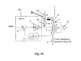
- FIGS. 14 and 15 Further embodiments of the invention are disclosed in schematic form in FIGS. 14 and 15, in which an auto-transformer implementation and a low voltage implementation are shown respectively. Reference numbers in FIGS. 14 and 15 which are the same as in previous embodiments relate to the same components.
- the output of the opamp 2 is connected to the centre tapping of the 1:n transformer 3 .
- a 1 ⁇ : ⁇ auto-transformer 41 is connected to the output of opamp 2 .
- a termination resistor 7 is connected between the 1:n transformer 3 and a centre tapping of the autotransformer 41 .
- one winding 43 of autotransformer 41 is connected in series with the termination resistor 7 and the other winding 44 is connected in parallel.
- the current to ground through the autotransformer 41 induces a voltage across one of its windings 43 which reduces the voltage drop across the termination resistor 7 thus reducing its power consumption—an aspect of all the embodiments of the present invention.
- feedback 13 is provided to match receive impedance.
- the output of the amplifier 2 is connected to a primary winding 45 of a back transformer 42 whose secondary windings have a turn ratio of 1 ⁇ : ⁇ .
- the termination impedance 7 is connected between a centre tapping of the back transformer secondary windings 43 , 44 and a primary winding 4 of a splitting (1:n) transformer 3 .
- the back-termination transformer 42 is included in a feedback loop which provides feedback 15 to the input side of the op-amp 2 , such that the line driver can be implemented using an operational amplifier 2 which operates off a low voltage supply, such as for example a voltage in the region of +/ ⁇ 5 or 6V.
- the gain K of the opamp 2 is assumed very large.
- the nullator operation of the amplifier imposes a voltage at node 3 equal to the amplifier output voltages of FIG. 12 .
- the auto-transformer two-port ( 43 , 44 ) is equivalent to the transformer ( 7 , 24 ) at FIG. 12 . So the operation will be equivalent.
- FIG. 16 A conventional line drive is shown in FIG. 16 with an amplifier 2 , a termination portion 10 , a signal portion 17 , a receive output 12 and a line 9 connected to the signal portion 17 .
- the currents through the two secondary windings of the matching transformer 3 are equal and opposite such that they compensate for each other in their respective windings of the receiver line transformer 14 .
- FIG. 17 is a further embodiment of the present invention and is an implementation of the circuit shown in FIG. 12 .
- the introduction of the (1: ⁇ ) back-termination transformer 22 into the termination portion 10 reduces the power dissipating part of the termination resistance R term to (1 ⁇ ).R ref .
- R term the power dissipating part of the termination resistance
- R ref the power dissipating part of the termination resistance
- the currents are not equal and opposite in the secondary windings of transformer 3 .
- This has to be compensated by some active component.
- This active component is conveniently the amplifier 2 although the present invention does not exclude a second amplifier for this job.
- a feedback factor 13 of ⁇ /2(1 ⁇ ) is applied to ensure correct impedance matching during reception.
- the feedback 13 is supplied from the output side of the transformer 3 however as indicated above the feedback may be obtained at any position of the circuit influenced by the receive signals.
- FIGS. 18 a and b a simpler version equivalent to the embodiment of FIG. 17 is disclosed, in which only two transformers are needed.
- the power dissipating impedance 7 of the termination portion 10 has the value (1 ⁇ ).R ref .
- the turns ratio of the first transformer 3 is altered in order to incorporate the back transformer into this transformer 3 . In this manner, a complete analogue front end can be implemented with only two transformers.
- FIG. 18 b shows a circuit based on the scheme shown in FIG. 18 a for feeding a 100 ohm transmission line.
- FIG. 19 the traditional hybrid line driver has been drawn showing a simple series termination.
- the power is transmitted through the termination impedance 7 as the value of R H is much higher than the values of resistance 7 or 8 .
- the resistors R H and the impedances 7 and 8 form voltage dividers in parallel which cancel out any effect of the amplifier 2 .
- FIG. 20 comprises a diagram of how the circuit of FIGS. 8 to 12 can be applied to this simple series termination.
- the back-termination of the present invention recuperates at least part of the current which is traditionally lost to the power dissipating termination impedance and gives that recovered current back to the active element (op-amp 2 ).
- the line transformer (1:1:N) may be operated as a common mode choke.
- a feedback 13 is fed back to the input of an active element, e.g. amplifier 2 , from the signal portion of the circuit.
- the present invention is particularly useful for implementation as part of a modem for use in broadband communications, such as for example xDSL communication. It may be found that the active back-termination of this invention is more space consuming than, for example, the resistive back termination of EP0901221 because of the bulkiness of the additional transformer (1: ⁇ ). If this turns out to be the case, it might be found useful to implement the line driver/modem of this invention at the customer premises (CPE) rather than at the central office (CO) side.
- CPE customer premises
- CO central office
Landscapes
- Engineering & Computer Science (AREA)
- Power Engineering (AREA)
- Computer Networks & Wireless Communication (AREA)
- Signal Processing (AREA)
- Dc Digital Transmission (AREA)
- Logic Circuits (AREA)
- Cable Transmission Systems, Equalization Of Radio And Reduction Of Echo (AREA)
- Circuit Arrangement For Electric Light Sources In General (AREA)
- Networks Using Active Elements (AREA)
Applications Claiming Priority (3)
| Application Number | Priority Date | Filing Date | Title |
|---|---|---|---|
| EP02290010A EP1326390B1 (de) | 2002-01-04 | 2002-01-04 | Impendanzanpassung für Leitungstreiber |
| EP02290010 | 2002-01-04 | ||
| EP02290010.4 | 2002-01-04 |
Publications (2)
| Publication Number | Publication Date |
|---|---|
| US20030128057A1 US20030128057A1 (en) | 2003-07-10 |
| US6825686B2 true US6825686B2 (en) | 2004-11-30 |
Family
ID=8185686
Family Applications (1)
| Application Number | Title | Priority Date | Filing Date |
|---|---|---|---|
| US10/335,903 Expired - Fee Related US6825686B2 (en) | 2002-01-04 | 2003-01-03 | Line interface circuit, associated line drivers and methods of operating the same |
Country Status (4)
| Country | Link |
|---|---|
| US (1) | US6825686B2 (de) |
| EP (1) | EP1326390B1 (de) |
| AT (1) | ATE314769T1 (de) |
| DE (1) | DE60208324T2 (de) |
Families Citing this family (4)
| Publication number | Priority date | Publication date | Assignee | Title |
|---|---|---|---|---|
| GB2413746B (en) | 2004-05-01 | 2007-02-14 | Abb Offshore Systems Ltd | Modem |
| EP1612962B1 (de) * | 2004-06-29 | 2011-09-28 | Lantiq Deutschland GmbH | Breitbandiger xSDL-Transceiver |
| CN105577126B (zh) * | 2015-12-15 | 2019-07-02 | 清华大学 | 石墨烯传输线作级间匹配的分布式放大器电路拓扑结构 |
| CN110838675B (zh) * | 2019-11-14 | 2020-09-08 | 安徽传矽微电子有限公司 | 一种高速大电流激光器驱动电路及其芯片 |
Citations (7)
| Publication number | Priority date | Publication date | Assignee | Title |
|---|---|---|---|---|
| US5856758A (en) | 1996-11-20 | 1999-01-05 | Adtran, Inc. | Low distortion driver employing positive feedback for reducing power loss in output impedance that effectively matches the impedance of driven line |
| EP0901221A1 (de) | 1997-09-05 | 1999-03-10 | Alcatel | Differenzausgangsverstärkeranordnung und Verfahren zur Abstimmung der Ausgangsimpedanz für einen solchen Verstärker |
| EP1039702A1 (de) | 1999-03-25 | 2000-09-27 | Nortel Networks Limited | Impendanzanpassung für Leitungstreiber |
| US6218872B1 (en) * | 1999-12-23 | 2001-04-17 | Orckit Communications Ltd. | Line driver with output impedance synthesis |
| US20020034294A1 (en) * | 2000-07-24 | 2002-03-21 | Alcatel | Low voltage broadband line driver |
| US20020090026A1 (en) * | 1998-07-31 | 2002-07-11 | Ashley Francis R. | Transceiver circuit and method |
| US6566947B2 (en) * | 2000-12-26 | 2003-05-20 | Nortel Networks Limited | Combined active impedance and filter in line drivers |
-
2002
- 2002-01-04 AT AT02290010T patent/ATE314769T1/de not_active IP Right Cessation
- 2002-01-04 EP EP02290010A patent/EP1326390B1/de not_active Expired - Lifetime
- 2002-01-04 DE DE60208324T patent/DE60208324T2/de not_active Expired - Fee Related
-
2003
- 2003-01-03 US US10/335,903 patent/US6825686B2/en not_active Expired - Fee Related
Patent Citations (9)
| Publication number | Priority date | Publication date | Assignee | Title |
|---|---|---|---|---|
| US5856758A (en) | 1996-11-20 | 1999-01-05 | Adtran, Inc. | Low distortion driver employing positive feedback for reducing power loss in output impedance that effectively matches the impedance of driven line |
| EP0901221A1 (de) | 1997-09-05 | 1999-03-10 | Alcatel | Differenzausgangsverstärkeranordnung und Verfahren zur Abstimmung der Ausgangsimpedanz für einen solchen Verstärker |
| US6097245A (en) * | 1997-09-05 | 2000-08-01 | Alcatel | Differential output amplifier arrangement and method for tuning the output impedance of a differential output amplifier |
| US20020090026A1 (en) * | 1998-07-31 | 2002-07-11 | Ashley Francis R. | Transceiver circuit and method |
| EP1039702A1 (de) | 1999-03-25 | 2000-09-27 | Nortel Networks Limited | Impendanzanpassung für Leitungstreiber |
| US6665399B1 (en) * | 1999-03-25 | 2003-12-16 | Nortel Networks Limited | High-efficiency line driver |
| US6218872B1 (en) * | 1999-12-23 | 2001-04-17 | Orckit Communications Ltd. | Line driver with output impedance synthesis |
| US20020034294A1 (en) * | 2000-07-24 | 2002-03-21 | Alcatel | Low voltage broadband line driver |
| US6566947B2 (en) * | 2000-12-26 | 2003-05-20 | Nortel Networks Limited | Combined active impedance and filter in line drivers |
Non-Patent Citations (3)
| Title |
|---|
| E. Nash, "Line-Driver Design for Broadband Communications Applications", Electronic Design Dec. 1, 1997, pp. 81-82,84, 86, 88, 90, 92, and 94. |
| M. Steffes, "Optimizing Performance in an xDSL Line Driver", Electronic Design, Apr. 19, 1999, pp. 44-49, 52-53, 56-59. |
| Schweber, Bill, et al.: "Analogue Front Ends Bridge the xDSL to Real World Chasm" EDN, Apr. 1, 1999, pp. 48-64. |
Also Published As
| Publication number | Publication date |
|---|---|
| EP1326390A1 (de) | 2003-07-09 |
| EP1326390B1 (de) | 2005-12-28 |
| ATE314769T1 (de) | 2006-01-15 |
| DE60208324D1 (de) | 2006-02-02 |
| US20030128057A1 (en) | 2003-07-10 |
| DE60208324T2 (de) | 2006-08-31 |
Similar Documents
| Publication | Publication Date | Title |
|---|---|---|
| CA1178386A (en) | Active impedance transformer assisted line feed circuit | |
| US6788745B1 (en) | Circuit and method for active termination of a transmission line | |
| US6756846B1 (en) | Increased output swing line drivers for operation at supply voltages that exceed the breakdown voltage of the integrated circuit technology | |
| JPS6141265A (ja) | 電話システム用電子バツテリーフイード回路 | |
| US6760434B1 (en) | Dual impedance hybrid | |
| US6825686B2 (en) | Line interface circuit, associated line drivers and methods of operating the same | |
| US5444777A (en) | Battery feed for telephone line cards | |
| JPS58501401A (ja) | 電話ライン回路 | |
| US6771770B2 (en) | Hybrid circuit for a broadband modem | |
| US20020151280A1 (en) | Line interface with gain feedback coupled matching impedance | |
| EP0163308B1 (de) | Speiseschaltung für ein Paar Teilnehmerleitungen | |
| EP0075914B1 (de) | Teilnehmeranschlussschaltung mit steuerbarem Gleichspannungswandler als Speiseschaltung | |
| US6218872B1 (en) | Line driver with output impedance synthesis | |
| US7212627B2 (en) | Line interface with analog echo cancellation | |
| US6999743B2 (en) | Line interface with second order high pass transfer function | |
| EP0186214B1 (de) | Speiseschaltung für eine Vermittlungsanlage | |
| US4767980A (en) | Inductance multiplier circuit | |
| US7577205B1 (en) | Return-loss compliant DSL modem line interface unit with complex termination | |
| JPS643387B2 (de) | ||
| US6563924B1 (en) | Subscriber matching circuit for electronic exchange | |
| TW584993B (en) | Echo cancelling arrangement | |
| JPH0468818B2 (de) | ||
| US6985578B2 (en) | Low voltage broadband line driver | |
| US20060023647A1 (en) | Line driver for an adaptive hybrid circuit | |
| JPH08172442A (ja) | 二線式のパルス信号伝送装置 |
Legal Events
| Date | Code | Title | Description |
|---|---|---|---|
| AS | Assignment |
Owner name: ALCATEL, FRANCE Free format text: ASSIGNMENT OF ASSIGNORS INTEREST;ASSIGNOR:DE WILDE, WIM ANDRE PAULA;REEL/FRAME:013853/0483 Effective date: 20020227 |
|
| FEPP | Fee payment procedure |
Free format text: PAYOR NUMBER ASSIGNED (ORIGINAL EVENT CODE: ASPN); ENTITY STATUS OF PATENT OWNER: LARGE ENTITY |
|
| REMI | Maintenance fee reminder mailed | ||
| LAPS | Lapse for failure to pay maintenance fees | ||
| STCH | Information on status: patent discontinuation |
Free format text: PATENT EXPIRED DUE TO NONPAYMENT OF MAINTENANCE FEES UNDER 37 CFR 1.362 |
|
| FP | Lapsed due to failure to pay maintenance fee |
Effective date: 20081130 |