US7628656B2 - Receptacle with crosstalk optimizing contact array - Google Patents
Receptacle with crosstalk optimizing contact array Download PDFInfo
- Publication number
- US7628656B2 US7628656B2 US11/372,957 US37295706A US7628656B2 US 7628656 B2 US7628656 B2 US 7628656B2 US 37295706 A US37295706 A US 37295706A US 7628656 B2 US7628656 B2 US 7628656B2
- Authority
- US
- United States
- Prior art keywords
- contact holes
- array
- contact
- array contacts
- contacts
- Prior art date
- Legal status (The legal status is an assumption and is not a legal conclusion. Google has not performed a legal analysis and makes no representation as to the accuracy of the status listed.)
- Expired - Lifetime
Links
Images


Classifications
-
- H—ELECTRICITY
- H01—ELECTRIC ELEMENTS
- H01R—ELECTRICALLY-CONDUCTIVE CONNECTIONS; STRUCTURAL ASSOCIATIONS OF A PLURALITY OF MUTUALLY-INSULATED ELECTRICAL CONNECTING ELEMENTS; COUPLING DEVICES; CURRENT COLLECTORS
- H01R12/00—Structural associations of a plurality of mutually-insulated electrical connecting elements, specially adapted for printed circuits, e.g. printed circuit boards [PCB], flat or ribbon cables, or like generally planar structures, e.g. terminal strips, terminal blocks; Coupling devices specially adapted for printed circuits, flat or ribbon cables, or like generally planar structures; Terminals specially adapted for contact with, or insertion into, printed circuits, flat or ribbon cables, or like generally planar structures
- H01R12/70—Coupling devices
- H01R12/71—Coupling devices for rigid printing circuits or like structures
-
- H—ELECTRICITY
- H01—ELECTRIC ELEMENTS
- H01R—ELECTRICALLY-CONDUCTIVE CONNECTIONS; STRUCTURAL ASSOCIATIONS OF A PLURALITY OF MUTUALLY-INSULATED ELECTRICAL CONNECTING ELEMENTS; COUPLING DEVICES; CURRENT COLLECTORS
- H01R13/00—Details of coupling devices of the kinds covered by groups H01R12/70 or H01R24/00 - H01R33/00
- H01R13/646—Details of coupling devices of the kinds covered by groups H01R12/70 or H01R24/00 - H01R33/00 specially adapted for high-frequency, e.g. structures providing an impedance match or phase match
- H01R13/6461—Means for preventing cross-talk
- H01R13/6467—Means for preventing cross-talk by cross-over of signal conductors
- H01R13/6469—Means for preventing cross-talk by cross-over of signal conductors on substrates
-
- H—ELECTRICITY
- H01—ELECTRIC ELEMENTS
- H01R—ELECTRICALLY-CONDUCTIVE CONNECTIONS; STRUCTURAL ASSOCIATIONS OF A PLURALITY OF MUTUALLY-INSULATED ELECTRICAL CONNECTING ELEMENTS; COUPLING DEVICES; CURRENT COLLECTORS
- H01R12/00—Structural associations of a plurality of mutually-insulated electrical connecting elements, specially adapted for printed circuits, e.g. printed circuit boards [PCB], flat or ribbon cables, or like generally planar structures, e.g. terminal strips, terminal blocks; Coupling devices specially adapted for printed circuits, flat or ribbon cables, or like generally planar structures; Terminals specially adapted for contact with, or insertion into, printed circuits, flat or ribbon cables, or like generally planar structures
- H01R12/50—Fixed connections
- H01R12/51—Fixed connections for rigid printed circuits or like structures
- H01R12/55—Fixed connections for rigid printed circuits or like structures characterised by the terminals
-
- H—ELECTRICITY
- H01—ELECTRIC ELEMENTS
- H01R—ELECTRICALLY-CONDUCTIVE CONNECTIONS; STRUCTURAL ASSOCIATIONS OF A PLURALITY OF MUTUALLY-INSULATED ELECTRICAL CONNECTING ELEMENTS; COUPLING DEVICES; CURRENT COLLECTORS
- H01R13/00—Details of coupling devices of the kinds covered by groups H01R12/70 or H01R24/00 - H01R33/00
- H01R13/646—Details of coupling devices of the kinds covered by groups H01R12/70 or H01R24/00 - H01R33/00 specially adapted for high-frequency, e.g. structures providing an impedance match or phase match
- H01R13/6473—Impedance matching
- H01R13/6477—Impedance matching by variation of dielectric properties
-
- H—ELECTRICITY
- H01—ELECTRIC ELEMENTS
- H01R—ELECTRICALLY-CONDUCTIVE CONNECTIONS; STRUCTURAL ASSOCIATIONS OF A PLURALITY OF MUTUALLY-INSULATED ELECTRICAL CONNECTING ELEMENTS; COUPLING DEVICES; CURRENT COLLECTORS
- H01R24/00—Two-part coupling devices, or either of their cooperating parts, characterised by their overall structure
- H01R24/60—Contacts spaced along planar side wall transverse to longitudinal axis of engagement
- H01R24/62—Sliding engagements with one side only, e.g. modular jack coupling devices
- H01R24/64—Sliding engagements with one side only, e.g. modular jack coupling devices for high frequency, e.g. RJ 45
-
- Y—GENERAL TAGGING OF NEW TECHNOLOGICAL DEVELOPMENTS; GENERAL TAGGING OF CROSS-SECTIONAL TECHNOLOGIES SPANNING OVER SEVERAL SECTIONS OF THE IPC; TECHNICAL SUBJECTS COVERED BY FORMER USPC CROSS-REFERENCE ART COLLECTIONS [XRACs] AND DIGESTS
- Y10—TECHNICAL SUBJECTS COVERED BY FORMER USPC
- Y10S—TECHNICAL SUBJECTS COVERED BY FORMER USPC CROSS-REFERENCE ART COLLECTIONS [XRACs] AND DIGESTS
- Y10S439/00—Electrical connectors
- Y10S439/941—Crosstalk suppression
Definitions
- This invention relates generally to electrical connectors, and more particularly, to a modular jack or receptacle with an array layout for reducing crosstalk.
- Various electronic systems such as those used to transmit signals in the telecommunications industry, include connector assemblies with electrical wires arranged in differential pairs.
- One wire in the differential pair carries a positive signal and the other wire carries a negative signal intended to have the same absolute magnitude, but at an opposite polarity.
- An RJ-45 electrical connector having a plug and outlet jack, is one example of a connector used to transmit electrical signals in differential pairs.
- An RJ-45 plug has four differential pairs of wires. The plug has a high level of noise due to the arrangement of the wires as determined by industry standards.
- EM electromagnetic
- Another problem experienced is mismatched impedance as a signal is transmitted through the plug and the receptacle assembly.
- the mismatched impedance causes a portion of the electrical signal to be reflected back toward its source.
- the amount of reflection that occurs due to impedance mismatch may be quantified as return loss.
- connector assemblies are being used to transmit data across higher frequencies and wider bandwidths. As frequencies increase, the system experiences more signal degradation due to EM signal coupling, return loss and impedance mismatch.
- a receptacle assembly comprises a housing having front and rear ends. The front end is configured to receive a plug and the rear end is configured to accept wire termination contacts.
- a circuit board has a plurality of contact holes and is held within the housing.
- a plurality of array contacts is arranged in a contact array within the housing.
- Each of the plurality of array contacts comprises a main section and a contact tail.
- the main section runs generally perpendicular to the circuit board.
- the contact tail has a first bend to form a first tail sub-section extending parallel to the circuit board and a second bend to form a second tail sub-section extending perpendicular to the circuit board.
- the second tail sub-section of each of the plurality of array contacts is received by one of the plurality of contact holes in the circuit board.
- a receptacle assembly comprises a housing having front and rear ends. The front end is configured to receive a plug and the rear end is configured to accept wire termination contacts.
- a circuit board is held within the housing and has first and second sides located opposite one another and top and bottom ends located opposite one another.
- the circuit board comprises a plurality of contact holes arranged in a contact array pattern and a plurality of wire termination contact holes arranged in a wire termination contact pattern.
- a plurality of array contacts is arranged in a contact array within the housing.
- the contact array comprises at least second and third differential pairs.
- the plurality of wire termination contact holes configured to receive the wire termination contacts associated with the second differential pair are located proximate the top end and the second side of the circuit board and the plurality of wire termination contact holes configured to receive the wire termination contacts associated with the third differential signal pair are located proximate the bottom end and the first side of the circuit board.
- FIG. 1 illustrates a perspective view of an outlet type receptacle assembly in accordance with an embodiment of the present invention.
- FIG. 2 illustrates the receptacle assembly of FIG. 1 with the housing removed in accordance with an embodiment of the present invention.
- FIG. 3 illustrates a front perspective view of a sub-assembly within the receptacle assembly of FIG. 1 in accordance with an embodiment of the present invention.
- FIG. 4 illustrates a front face of the circuit board of FIG. 2 in accordance with an embodiment of the present invention.
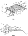
- FIG. 5 illustrates a rear perspective view of a contact array formed in accordance with an embodiment of the present invention.
- FIG. 6 illustrates a side view of the contact array of FIG. 5 formed in accordance with an embodiment of the present invention.
- FIG. 7 illustrates a rear perspective view of the sub-assembly of FIG. 2 in accordance with an embodiment of the present invention.
- FIG. 8 illustrates a contact entry pattern in accordance with an embodiment of the present invention.
- FIG. 1 illustrates a receptacle assembly 100 .
- the receptacle assembly 100 has a front end 102 and a rear end 114 .
- a housing 108 partially encloses a contact array 106 within a cavity 110 .
- the cavity 110 accepts an RJ-45 plug (not shown) inserted through the front end 102 .
- the RJ-45 plug has contacts which electrically interface with the contact array 106 .
- a circuit board 148 ( FIG. 2 ) is mounted within the housing 108 proximate a housing rear end 104 .
- a front end 116 of a wire connector housing 112 mates to the housing rear end 104 .
- the wire connector housing 112 accepts wires from a cable (not shown) through rear end 114 which electrically interface with wire termination contacts 113 held within the wire connector housing 112 .
- FIG. 2 illustrates the receptacle assembly 100 of FIG. 1 with the housing 108 removed.
- the wire termination contacts 113 are accepted by wire termination contact holes (illustrated in FIGS. 3 and 4 ) in the circuit board 148 and establish contact with conductive material on the circuit board 148 .
- the wire termination contacts 113 are insulation displacement contacts (IDCs), however, other connection means may be used.
- IDCs insulation displacement contacts
- the wires within the cable terminate at an IDC end of the IDC contacts.
- the opposite end of the IDC contacts interface with the circuit board 148 within the wire termination contact holes.
- the wire termination contacts 113 terminate at the circuit board 148 with eye of the needle contacts, compliant pins, solder, press-in connection or other means known to those skilled in the art.
- FIG. 3 illustrates a front perspective view of a sub-assembly 120 within the receptacle assembly 100 of FIG. 1 .
- the sub-assembly 120 includes a base 122 which may be formed of plastic or other nonconductive material.
- the base 122 has a lead edge 103 facing and located proximate to the front end 102 ( FIG. 1 ) of the housing 108 and a rear edge 105 facing and located proximate to the housing rear end 104 .
- the base 122 may have a PCB surface on which the contact array 106 may lay.
- a circuit board (not shown) may be used instead of the base 122 to provide signal conditioning.
- the rear edge 105 includes posts 107 that are configured to be received in holes 109 in the front face 150 of the circuit board 148 .
- the posts 107 may perform alignment and/or locking functions, in order to position and hold the rear edge 105 against the front face 150 of the circuit board 148 in a desired alignment and orientation.
- the base 122 includes a series of parallel notches 123 formed therein which extend to the lead edge 103 and are spaced apart from one another in a desired manner.
- the base 122 also includes a bridge 125 located proximate the rear edge 105 .
- the bridge 125 has a series of posts 127 extending upward therefrom and spaced apart from one another by gaps 129 aligned with the notches 123 .
- the array contacts in the contact array 106 have an interference fit with the posts 127 and gaps 129 .
- the contact array 106 includes array contacts 124 , 126 , 128 , 130 , 132 , 134 , 136 and 138 that are arranged parallel to one another and oriented to extend from within the parallel notches 123 proximate the lead edge 103 to the rear edge 105 of the base 122 . Eight contacts are illustrated in the contact array 106 ; however, more or less than eight contacts may be used.
- Array contacts 124 and 126 form a first differential pair 140
- array contacts 128 and 134 form a second differential pair 142
- array contacts 130 and 132 form a third differential pair 144
- array contacts 136 and 138 form a fourth differential pair 146 .
- Array contacts 124 and 126 , 130 and 132 , and 136 and 138 of the first, third and fourth differential pairs 140 , 144 and 146 , respectively, are located immediately adjacent one another.
- the array contacts 128 and 134 of the second differential pair 142 are not located immediately adjacent one another. Instead, the array contacts 128 and 134 of the second differential pair 142 are split or separated from one another by intervening third differential pair 144 .
- the array contact 128 is adjacent to the array contacts 126 and 130 of the first and third differential pairs 140 and 144 , respectively, while the array-contact 134 is adjacent to the array contacts 132 and 136 of each of the third and fourth differential pairs 144 and 146 .
- the array contacts 124 , 126 , 128 , 130 , 132 , 134 , 136 and 138 extend along the base 122 in a co-planar arrangement and have contact tails 216 ( FIG. 5 ) that enter the circuit board 148 to define a contact entry pattern 153 ( FIG. 4 ).
- the contact tails 216 may be soldered to holes in the circuit board 148 or interconnect with the holes using a compliant pin design or other interconnection known in the art.
- circuit board 148 may vary in size, depending on customer specifications. For example, it may be desirable to make the receptacle assembly 100 as small or compact as possible. Also, further enhancements may be added to the circuit board 148 to modify the transmitted signals.
- FIG. 4 illustrates a front face 150 of the circuit board 148 of FIG. 2 .
- the circuit board 148 has a top end 160 and a bottom end 162 .
- Contact holes 188 , 190 , 192 , 194 , 196 , 198 , 200 and 202 form the contact entry pattern 153 , which is associated with a particular array layout.
- the contact entry pattern 153 is illustrated in a central portion 164 of the circuit board 148 , but may also be located in an off-center location, such as by shifting the contact entry pattern 153 upward, downward, left or right.
- the contact holes 188 , 190 , 192 , 194 , 196 , 198 , 200 and 202 accept the contact tails 216 of the array contacts 124 , 126 , 128 , 130 , 132 , 134 , 136 and 138 , respectively.
- Wire termination contact holes 170 , 172 , 174 , 176 , 178 , 180 , 182 , and 184 form a wire termination contact pattern 154 located in top and bottom portions 166 and 168 of the circuit board 148 for accepting the wire termination contacts 113 .
- Traces electrically connect each of the contact holes 188 , 190 , 192 , 194 , 196 , 198 , 200 and 202 within the central portion 164 with a corresponding one of the wire termination contact holes 170 , 172 , 174 , 176 , 178 , 180 , 182 , and 184 in either the top or bottom portion 166 or 168 .
- Each of the holes has been provided with a number (corresponding to a contact or pin) within FIG. 4 to illustrate one exemplary interconnection pattern.
- the contact hole 188 is electrically joined to wire termination contact hole 178
- contact hole 190 is electrically joined to wire termination contact hole 180 .
- Contact holes 192 , 194 , 196 , 198 , 200 and 202 are electrically joined to wire termination contact holes 170 , 174 , 176 , 172 , 182 and 184 , respectively.
- Other interconnection patterns may be used.
- FIG. 5 illustrates a view of the contact array 106 in accordance with an embodiment of the present invention.
- First, second and third sections 210 , 212 and 214 together form a main section 218 which is held generally perpendicular to the circuit board 148 .
- the array contacts 124 , 126 , 128 , 130 , 132 , 134 , 136 and 138 extend planar to the base 122 ( FIG. 3 ) and normal to the circuit board 148 .
- the pairs of array contacts 124 and 126 , 130 and 132 , and 136 and 138 cross over each other, while the array contacts 128 and 134 continue planar to the base 122 .
- the cross-over pattern compensates for a portion of the crosstalk generated in the plug.
- the array contacts 124 , 126 , 128 , 130 , 132 , 134 , 136 and 138 extend planar to the base 122 .
- Each of the array contacts 124 , 126 , 128 , 130 , 132 , 134 , 136 and 138 has a contact tail 216 .
- Each contact tail 216 is bent to form a first bend 224 of approximately 90 degrees, wherein the array contacts 124 , 128 , 132 and 136 are bent in an upward direction as indicated by arrow A and the array contacts 126 , 130 , 134 and 138 are bent in a downward direction as indicated by arrow B.
- a first tail sub-section 228 extends upwards or downwards, parallel to the circuit board 148 for one of two distances, and then a second bend 226 of approximately 90 degrees is formed.
- a second tail sub-section 222 extends perpendicular to the circuit board 148 and through one of the contact holes 188 , 190 , 192 , 194 , 196 , 198 , 200 and 202 in the circuit board 148 , forming the contact entry pattern 153 ( FIG. 4 ), which is discussed further below.
- FIG. 6 illustrates a side view of the contact array 106 in accordance with an embodiment of the present invention.
- First, second, and third sections 210 , 212 , and 214 and contact tails 216 are illustrated with like item numbers.
- Plane 220 illustrates a plane substantially parallel to the plane of the main section 218 , which is perpendicular to the circuit board 148 .
- the second tail sub-sections 222 extend in four parallel rows formed at distances D 1 , D 2 , D 3 and D 4 from the plane 220 .
- Distances D 1 and D 4 are larger than distances D 2 and D 3 . Also, distances D 1 and D 4 are equal to each other and distances D 2 and D 3 are equal to each other.
- FIG. 7 illustrates a rear perspective view of the sub-assembly 120 of FIG. 3 to better show the contact entry pattern 153 of the second tail sub-sections 222 .
- a rear face 152 of the circuit board 148 is shown.
- the second tail sub-sections 222 enter the contact holes 188 , 190 , 192 , 194 , 196 , 198 , 200 and 202 in the front face 150 and may extend through and beyond the rear face 152 of the circuit board 148 .
- the second tail sub-sections 222 may be soldered to the circuit board 148 , or may be compliant pin, eye of the needle, or other type of connection known in the art.
- the spatial relationship of the contact holes 188 , 190 , 192 , 194 , 196 , 198 , 200 and 202 with respect to one another and the spatial relationship of the wire termination contact holes 170 , 172 , 174 , 176 , 178 , 180 , 182 , and 184 with respect to one another is determined to achieve a desired electrical performance.
- the contact holes 188 , 190 , 192 , 194 , 196 , 198 , 200 and 202 and wire termination contact holes 170 , 172 , 174 , 176 , 178 , 180 , 182 , and 184 may form patterns for coupling and isolating certain contacts.
- the wire termination contact pattern 154 will be discussed first, while the contact entry pattern 153 will be discussed further below.
- the two wires of each wire pair are twisted together.
- the wires are paired as wire pairs 1 / 2 , 3 / 6 , 4 / 5 and 7 / 8 , which are associated with the first, second, third and fourth differential pairs 140 , 142 , 144 and 146 , respectively.
- Each wire pair is received by wire termination contact holes located proximate different corners of the board 148 .
- wire pair 1 / 2 is received by wire termination contact holes 178 and 180 proximate a first corner
- wire pair 3 / 6 is received by wire termination contact holes 170 and 172 proximate a second corner
- wire pair 7 / 8 is received by wire termination contact holes 182 and 184 proximate a third corner
- wire pair 4 / 5 is received by wire termination contact holes 174 and 176 proximate a fourth corner.
- wire termination contact holes 170 , 172 , 174 , 176 , 178 , 180 , 182 , and 184 are arranged, in part, to avoid creating additional noise in the receptacle assembly 100 .
- the plug contains sizable noise with the most noise occurring between the differential pairs 142 and 144 . Because this pair combination has the most noise, the wire termination contact pattern 154 isolates the wire pairs 3 / 6 and 4 / 5 from one another. Referring to FIG. 4 , wire termination contact holes 170 and 172 accept wire termination contacts 113 interconnected with wire pair 3 / 6 , and wire termination contact holes 174 and 176 accept wire termination contacts 113 interconnected with wire pair 4 / 5 .
- Wire termination contact holes 170 and 172 are positioned in one corner of the top portion 166 while the wire termination contact holes 174 and 176 are positioned in the opposite corner, respectively, of the bottom portion 168 , isolating the second and third differential pairs from one another. In other words, the second and third differential pairs are located far apart from one another on the circuit board 148 .
- the wire termination contact pattern 154 also takes into consideration the ease of connecting the cable to the receptacle assembly 100 .
- Two color schemes determined by industry standards for the RJ-45 are called 568 A and 568 B and match pin numbers to wire colors of a cable.
- Two sets of wire pairs are typically designated specific colors, and therefore, within the cable, wire pair 4 / 5 is blue, and wire pair 7 / 8 is brown.
- wire pair 4 / 5 is blue
- wire pair 7 / 8 is brown.
- wire pair 1 / 2 is green
- wire pair 3 / 6 is orange.
- wire pair 1 / 2 is orange and wire pair 3 / 6 is green.
- Another consideration relates to the orientation of the wires within the cable jacket.
- a common wire color breakout is blue-orange-green-brown that rotates either in the clockwise (CW) or counter-clockwise (CCW) direction depending upon which end of the cable is being viewed. Therefore, there are four main patterns that may be presented: A-pattern and CCW, A-pattern and CW, B-pattern and CCW and B-pattern and CW.
- the wire termination contact pattern 154 was chosen so that one of these four main patterns matches directly to the jack without the need for altering or crossing over the wire pairs within the natural orientation of the cable resulting in ease of installation where possible.
- the pattern chosen for this embodiment was B-pattern and CCW.
- the wire termination contact pattern 154 further improves performance by separating noisy pairs.
- the wire pair 4 / 5 is blue and corresponds to the wire termination contact holes 174 and 176
- the wire pair 3 / 6 corresponds to the wire termination contact holes 170 and 172 , which are located in an opposite corner of the board 148 with respect to the wire termination contact holes 174 and 176 .
- the wire pair 3 / 6 may be either green or orange. Therefore, in one embodiment, the wire pair 1 / 2 is orange and corresponds to wire termination contact holes 178 and 180 , while the wire pair 3 / 6 is green and corresponds to wire termination contact holes 170 and 172 . In another embodiment, the wire pair 1 / 2 may be green while the wire pair 3 / 6 may be orange.
- the contact entry pattern 153 will now be discussed.
- one of the four differential pairs is split around another.
- Industry standards require a split pair and also dictate how much noise needs to occur in the plug.
- the highest degree of crosstalk is created between these two pairs, but the other pair combinations also exhibit crosstalk that is not insignificant. This is partly due to the large parallel blades in the plug, and sometimes, the parallel nature of the wires as they are dressed into the plug. Therefore, it is desirable to counteract this noise in the receptacle assembly 100 , such as through compensation in the receptacle assembly 100 , so the mated connector (the plug and the receptacle assembly 100 joined together) has a significantly smaller amount of noise than the plug alone.
- FIG. 8 illustrates relationships between and groupings of the contact holes 188 , 190 , 192 , 194 , 196 , 198 , 200 and 202 within the contact entry pattern 153 .
- Each of the contact holes 188 , 190 , 192 , 194 , 196 , 198 , 200 and 202 has a center 262 .
- Circles and lines are used to show relationships and/or distances between the centers 262 of the contact holes 188 , 190 , 192 , 194 , 196 , 198 , 200 and 202 , and therefore the circles and lines themselves do not form a part of the contact entry pattern 153 .
- a first group 230 includes the contact holes 188 , 192 and 196 arranged in a triangular layout.
- a circle 232 which may have a minimum diameter of 0.04 inch, captures the center 262 of each of the contact holes 188 , 192 and 196 . In one embodiment, the circle 232 may have a diameter of 0.082 inch. Optionally, the circle 232 may have a diameter of up to 0.140 inch.
- a second group 234 includes the contact holes 194 , 198 and 202 which are also arranged in a triangular layout.
- a circle 236 captures the center 262 of each of the contact holes 194 , 198 and 202 and may also have a diameter from 0.04 inch to 0.140 inch.
- the contact entry pattern 153 may be further described by referring again to FIG. 6 .
- the plane 220 has been indicated on FIG. 8 .
- a first subset 254 includes the contact holes 200 , 196 and 188 , and the center 262 of each is the distance D 1 from the plane 220 .
- a second subset 256 includes contact hole 192 , the center 262 of which is the distance D 2 from the plane 220 .
- Third subset 258 includes contact hole 198 , the center 262 of which is the distance D 3 from the plane 220 .
- Fourth subset 260 includes contact holes 202 , 194 and 190 , and the center 262 of each is the distance D 4 from the plane 220 .
- the distances D 1 and D 4 are equal to each other and distances D 2 and D 3 are equal to each other.
- blades 3 and 4 and blades 5 and 6 have the greatest level of noise due to their close proximity with each other.
- the array contacts' 128 and 130 and the array contacts 132 and 134 experience a higher level of noise due to their close proximity to one another. It is desired to isolate the sets of contacts experiencing the higher level of noise.
- the array contacts 128 and 130 are received by the contact holes 192 and 194 , respectively, which are located away from each other, and the array contacts 132 and 134 are received by contact holes 196 and 198 , respectively, which are located away from each other.
- line 246 extends between the centers 262 of the contact holes 192 and 194 and line 248 extends between the centers 262 of the contact holes 196 and 198 , illustrating a distance between the centers 262 of the respective contact holes, which may be from 0.120 inch to 0.20 inch. In one embodiment, the distance may be 0.160 inch.
- the noise in the receptacle assembly 100 may be further counteracted through compensation by placing other array contacts close to one another.
- the array contacts 128 and 132 are received by contact holes 192 and 196 , respectively, which are located in close proximity to each other, and the array contacts 130 and 134 are received by contact holes 194 and 198 , respectively, which are located in close proximity to each other.
- line 238 extends between the centers 262 of the contact holes 192 and 196 and line 240 extends between the centers 262 of the contact holes 194 and 198 , illustrating a distance between the centers 262 of the respective contact holes which may be from 0.02 inch to 0.100 inch. In one embodiment, the distance may be 0.064 inch.
- the second differential pair (blades 3 / 6 ) experiences a high level of noise with both the first differential pair (blades 1 / 2 ) and fourth differential pair (blades 7 / 8 ) due to their proximity in the plug and because the second differential pair is a split pair.
- the array contacts 126 and 128 are received by contact holes 190 and 192 , respectively, which are located away from each other, and array contacts 134 and 136 are received by contact holes 198 and 200 , respectively, which are located away from each other.
- line 250 extends between the centers 262 of the contact holes 190 and 192 and line 252 extends between the centers 262 of the contact holes 198 and 200 , illustrating a distance between the centers 262 of the respective contact holes, which may be from 0.120 inch to 0.20 inch.
- contact holes 188 and 192 receiving array contacts 124 and 128 , respectively, and contact holes 198 and 202 receiving array contacts 134 and 138 , respectively, are placed in closer proximity to one another on the circuit board 148 .
- line 242 extends between the centers 262 of the contact holes 188 and 192 and line 244 extends between the centers 262 of the contact holes 198 and 202 , illustrating a distance between the centers 262 of the respective contact holes, which may be from 0.02 inch to 0.100 inch.
- a signal sent down two pins (or contacts or wires) in a differential pair has an impedance based on at least one of cross-section of the conductor, space between the conductors and the dielectric constant separating the two conductors in a pair.
- the adjacent array contacts of the first, third and fourth differential pairs 140 , 144 and 146 have essentially the same geometry, and are close together in the receptacle assembly 100 , resulting in an impedance between the array contacts of each pair that is lower than desired.
- contact holes 200 and 202 receiving array contacts 136 and 138 , respectively, of the fourth differential pair are placed farther apart with respect to each other, as are contact holes 188 and 190 receiving array contacts 124 and 126 , respectively, of the first differential pair, and contact holes 194 and 196 receiving array contacts 130 and 132 , respectively, of the third differential pair.
- Distance between the contact holes of a differential pair may be increased to increase the impedance, providing a more favorable return loss.
Landscapes
- Details Of Connecting Devices For Male And Female Coupling (AREA)
- Coupling Device And Connection With Printed Circuit (AREA)
- Connector Housings Or Holding Contact Members (AREA)
Priority Applications (14)
| Application Number | Priority Date | Filing Date | Title |
|---|---|---|---|
| US11/372,957 US7628656B2 (en) | 2006-03-10 | 2006-03-10 | Receptacle with crosstalk optimizing contact array |
| TW096108166A TWI383546B (zh) | 2006-03-10 | 2007-03-09 | 具有串音最佳化的接點陣列之插座 |
| KR1020087022862A KR101038375B1 (ko) | 2006-03-10 | 2007-03-09 | 크로스토크를 최적화하는 콘택 어레이를 갖는 리셉터클 |
| PCT/US2007/006123 WO2007106409A1 (fr) | 2006-03-10 | 2007-03-09 | Prise de courant avec rangée de contacts d'optimisation de diaphonie |
| CN2007800165445A CN101438468B (zh) | 2006-03-10 | 2007-03-09 | 具有串扰优化触点阵列的插座 |
| BRPI0708730A BRPI0708730B1 (pt) | 2006-03-10 | 2007-03-09 | receptáculo com conjunto de contatos otimizando diafonia |
| JP2008558428A JP4776041B2 (ja) | 2006-03-10 | 2007-03-09 | クロストーク最適化コンタクトアレーを有するリセプタクル |
| MX2008011542A MX2008011542A (es) | 2006-03-10 | 2007-03-09 | Receptaculo con arreglo de contacto para optimizacion de interferencia. |
| ES07752799.2T ES2539638T3 (es) | 2006-03-10 | 2007-03-09 | Receptáculo con conjunto geométricamente ordenado de contactos para la optimización de la diafonía |
| EP07752799.2A EP1997195B1 (fr) | 2006-03-10 | 2007-03-09 | Prise de courant avec rangée de contacts d'optimisation de diaphonie |
| AU2007225240A AU2007225240B8 (en) | 2006-03-10 | 2007-03-09 | Receptacle with crosstalk optimizing contact array |
| PL07752799T PL1997195T3 (pl) | 2006-03-10 | 2007-03-09 | Wtyczka z układem styków optymalizującym przesłuchy |
| CA2646025A CA2646025C (fr) | 2006-03-10 | 2007-03-09 | Prise de courant avec rangee de contacts d'optimisation de diaphonie |
| ARP070101012A AR059827A1 (es) | 2006-03-10 | 2007-03-12 | Receptaculo con contactos que optimizan el acople indeseado de senales electromagneticas |
Applications Claiming Priority (1)
| Application Number | Priority Date | Filing Date | Title |
|---|---|---|---|
| US11/372,957 US7628656B2 (en) | 2006-03-10 | 2006-03-10 | Receptacle with crosstalk optimizing contact array |
Publications (2)
| Publication Number | Publication Date |
|---|---|
| US20070212946A1 US20070212946A1 (en) | 2007-09-13 |
| US7628656B2 true US7628656B2 (en) | 2009-12-08 |
Family
ID=38169422
Family Applications (1)
| Application Number | Title | Priority Date | Filing Date |
|---|---|---|---|
| US11/372,957 Expired - Lifetime US7628656B2 (en) | 2006-03-10 | 2006-03-10 | Receptacle with crosstalk optimizing contact array |
Country Status (14)
| Country | Link |
|---|---|
| US (1) | US7628656B2 (fr) |
| EP (1) | EP1997195B1 (fr) |
| JP (1) | JP4776041B2 (fr) |
| KR (1) | KR101038375B1 (fr) |
| CN (1) | CN101438468B (fr) |
| AR (1) | AR059827A1 (fr) |
| AU (1) | AU2007225240B8 (fr) |
| BR (1) | BRPI0708730B1 (fr) |
| CA (1) | CA2646025C (fr) |
| ES (1) | ES2539638T3 (fr) |
| MX (1) | MX2008011542A (fr) |
| PL (1) | PL1997195T3 (fr) |
| TW (1) | TWI383546B (fr) |
| WO (1) | WO2007106409A1 (fr) |
Cited By (8)
| Publication number | Priority date | Publication date | Assignee | Title |
|---|---|---|---|---|
| US20110250802A1 (en) * | 2009-08-25 | 2011-10-13 | Tyco Electronics Corporation | Electrical connector with separable contacts |
| US8282425B2 (en) | 2009-08-25 | 2012-10-09 | Tyco Electronics Corporation | Electrical connectors having open-ended conductors |
| US8568177B2 (en) | 2010-08-03 | 2013-10-29 | Tyco Electronics Corporation | Electrical connectors and printed circuits having broadside-coupling regions |
| US20150222056A1 (en) * | 2012-08-07 | 2015-08-06 | Tyco Electronics (Shanghai) Co. Ltd., | Electrical Connector and Conductive Terminal Assembly Thereof |
| US9379500B2 (en) | 2013-03-11 | 2016-06-28 | Panduit Corp. | Front sled assemblies for communication jacks and communication jacks having front sled assemblies |
| US9577383B2 (en) | 2006-04-11 | 2017-02-21 | Commscope Technologies Llc | Telecommunications device |
| US9608378B2 (en) | 2008-02-12 | 2017-03-28 | Commscope Technologies Llc | Multistage capacitive crosstalk compensation arrangement |
| US11817656B2 (en) | 2021-01-18 | 2023-11-14 | Foxconn (Kunshan) Computer Connector Co., Ltd. | Electrical connector having overlapping coupling portions |
Families Citing this family (18)
| Publication number | Priority date | Publication date | Assignee | Title |
|---|---|---|---|---|
| TWM301448U (en) * | 2006-06-02 | 2006-11-21 | Jyh Eng Technology Co Ltd | Network connector |
| US7364470B2 (en) * | 2006-07-05 | 2008-04-29 | Commscope, Inc. Of North Carolina | Communications connectors with signal current splitting |
| US7427218B1 (en) * | 2007-05-23 | 2008-09-23 | Commscope, Inc. Of North Carolina | Communications connectors with staggered contacts that connect to a printed circuit board via contact pads |
| US7914346B2 (en) * | 2008-11-04 | 2011-03-29 | Commscope, Inc. Of North Carolina | Communications jacks having contact wire configurations that provide crosstalk compensation |
| US7682203B1 (en) * | 2008-11-04 | 2010-03-23 | Commscope, Inc. Of North Carolina | Communications jacks having contact wire configurations that provide crosstalk compensation |
| KR101000253B1 (ko) | 2009-06-22 | 2010-12-10 | 현대자동차주식회사 | 다선식 커넥터 |
| US8128436B2 (en) * | 2009-08-25 | 2012-03-06 | Tyco Electronics Corporation | Electrical connectors with crosstalk compensation |
| JP5400849B2 (ja) * | 2011-10-05 | 2014-01-29 | ヒロセ電機株式会社 | 接続ブレード及びこれを有する中間接続電気コネクタそしてこれらを有する接続ブレード組立体 |
| CN103545664A (zh) * | 2012-07-12 | 2014-01-29 | 富士康(昆山)电脑接插件有限公司 | Rj插头连接器 |
| KR101994984B1 (ko) | 2012-07-16 | 2019-07-01 | 콤스코프 인코포레이티드 오브 노스 캐롤라이나 | 균형 잡힌 핀 및 소켓 커넥터들 |
| US9118134B2 (en) * | 2013-03-01 | 2015-08-25 | Panduit Corp. | RJ-45-compatible communication connector with contacts having wider distal ends |
| US8894447B2 (en) | 2013-03-14 | 2014-11-25 | Commscope, Inc. Of North Carolina | Communication plug having a plurality of coupled conductive paths |
| US9514966B2 (en) * | 2014-04-11 | 2016-12-06 | Qualcomm Incorporated | Apparatus and methods for shielding differential signal pin pairs |
| CN104409926B (zh) * | 2014-11-21 | 2017-12-12 | 华为技术有限公司 | 一种改善SAS连接器串扰的方法及Mini SAS连接器 |
| JP6655183B2 (ja) * | 2015-11-11 | 2020-02-26 | ベル フューズ (マカオ コマーシャル オフショア) リミテッド | モジュラーコネクタ |
| JP6744835B2 (ja) * | 2017-03-31 | 2020-08-19 | モレックス エルエルシー | コネクタ |
| US10530106B2 (en) | 2018-01-31 | 2020-01-07 | Bel Fuse (Macao Commercial Offshore) Limited | Modular plug connector with multilayer PCB for very high speed applications |
| CN110994230B (zh) * | 2018-12-28 | 2021-06-18 | 富鼎精密工业(郑州)有限公司 | 电连接器 |
Citations (14)
| Publication number | Priority date | Publication date | Assignee | Title |
|---|---|---|---|---|
| US5626497A (en) | 1994-07-14 | 1997-05-06 | Molex Incorporated | Modular jack type connector |
| US5941734A (en) * | 1995-12-25 | 1999-08-24 | Matsushita Electric Works, Ltd. | Connector |
| US6139368A (en) * | 1998-12-21 | 2000-10-31 | Thomas & Betts International, Inc. | Filtered modular connector |
| US6190211B1 (en) | 2000-02-23 | 2001-02-20 | Telebox Industries Corp. | Isolation displacement connector |
| US6196880B1 (en) | 1999-09-21 | 2001-03-06 | Avaya Technology Corp. | Communication connector assembly with crosstalk compensation |
| US6464541B1 (en) | 2001-05-23 | 2002-10-15 | Avaya Technology Corp. | Simultaneous near-end and far-end crosstalk compensation in a communication connector |
| US20030003810A1 (en) * | 2001-06-28 | 2003-01-02 | Arnould Fabrique D'appareillage Electrique | Low-current female socket of the modular jack type |
| US6530810B2 (en) * | 2000-09-19 | 2003-03-11 | Avaya Technology Corp. | High performance communication connector construction |
| US6558207B1 (en) * | 2000-10-25 | 2003-05-06 | Tyco Electronics Corporation | Electrical connector having stamped electrical contacts with deformed sections for increased stiffness |
| US6592395B2 (en) * | 2001-10-03 | 2003-07-15 | Avaya Technology Corp. | In-line cable connector assembly |
| US6896557B2 (en) * | 2001-03-28 | 2005-05-24 | Ortronics, Inc. | Dual reactance low noise modular connector insert |
| US6916209B1 (en) * | 2004-01-23 | 2005-07-12 | Molex Incorporated | Electrical signal transmission system |
| US7052328B2 (en) * | 2002-11-27 | 2006-05-30 | Panduit Corp. | Electronic connector and method of performing electronic connection |
| US7264516B2 (en) * | 2004-12-06 | 2007-09-04 | Commscope, Inc. | Communications jack with printed wiring board having paired coupling conductors |
Family Cites Families (4)
| Publication number | Priority date | Publication date | Assignee | Title |
|---|---|---|---|---|
| US5586914A (en) * | 1995-05-19 | 1996-12-24 | The Whitaker Corporation | Electrical connector and an associated method for compensating for crosstalk between a plurality of conductors |
| CN100508016C (zh) * | 2003-02-07 | 2009-07-01 | 三洋电机株式会社 | 显示装置中的色空间补偿电路 |
| TWM266616U (en) * | 2004-11-01 | 2005-06-01 | Plastron Prec Co Ltd | Signal connector structure |
| TWM277168U (en) * | 2005-05-18 | 2005-10-01 | Telebox Ind Corp | Shielding shell for low crosstalk connector |
-
2006
- 2006-03-10 US US11/372,957 patent/US7628656B2/en not_active Expired - Lifetime
-
2007
- 2007-03-09 CA CA2646025A patent/CA2646025C/fr active Active
- 2007-03-09 WO PCT/US2007/006123 patent/WO2007106409A1/fr not_active Ceased
- 2007-03-09 TW TW096108166A patent/TWI383546B/zh not_active IP Right Cessation
- 2007-03-09 JP JP2008558428A patent/JP4776041B2/ja active Active
- 2007-03-09 EP EP07752799.2A patent/EP1997195B1/fr active Active
- 2007-03-09 CN CN2007800165445A patent/CN101438468B/zh active Active
- 2007-03-09 ES ES07752799.2T patent/ES2539638T3/es active Active
- 2007-03-09 BR BRPI0708730A patent/BRPI0708730B1/pt not_active IP Right Cessation
- 2007-03-09 AU AU2007225240A patent/AU2007225240B8/en active Active
- 2007-03-09 KR KR1020087022862A patent/KR101038375B1/ko active Active
- 2007-03-09 PL PL07752799T patent/PL1997195T3/pl unknown
- 2007-03-09 MX MX2008011542A patent/MX2008011542A/es active IP Right Grant
- 2007-03-12 AR ARP070101012A patent/AR059827A1/es active IP Right Grant
Patent Citations (14)
| Publication number | Priority date | Publication date | Assignee | Title |
|---|---|---|---|---|
| US5626497A (en) | 1994-07-14 | 1997-05-06 | Molex Incorporated | Modular jack type connector |
| US5941734A (en) * | 1995-12-25 | 1999-08-24 | Matsushita Electric Works, Ltd. | Connector |
| US6139368A (en) * | 1998-12-21 | 2000-10-31 | Thomas & Betts International, Inc. | Filtered modular connector |
| US6196880B1 (en) | 1999-09-21 | 2001-03-06 | Avaya Technology Corp. | Communication connector assembly with crosstalk compensation |
| US6190211B1 (en) | 2000-02-23 | 2001-02-20 | Telebox Industries Corp. | Isolation displacement connector |
| US6530810B2 (en) * | 2000-09-19 | 2003-03-11 | Avaya Technology Corp. | High performance communication connector construction |
| US6558207B1 (en) * | 2000-10-25 | 2003-05-06 | Tyco Electronics Corporation | Electrical connector having stamped electrical contacts with deformed sections for increased stiffness |
| US6896557B2 (en) * | 2001-03-28 | 2005-05-24 | Ortronics, Inc. | Dual reactance low noise modular connector insert |
| US6464541B1 (en) | 2001-05-23 | 2002-10-15 | Avaya Technology Corp. | Simultaneous near-end and far-end crosstalk compensation in a communication connector |
| US20030003810A1 (en) * | 2001-06-28 | 2003-01-02 | Arnould Fabrique D'appareillage Electrique | Low-current female socket of the modular jack type |
| US6592395B2 (en) * | 2001-10-03 | 2003-07-15 | Avaya Technology Corp. | In-line cable connector assembly |
| US7052328B2 (en) * | 2002-11-27 | 2006-05-30 | Panduit Corp. | Electronic connector and method of performing electronic connection |
| US6916209B1 (en) * | 2004-01-23 | 2005-07-12 | Molex Incorporated | Electrical signal transmission system |
| US7264516B2 (en) * | 2004-12-06 | 2007-09-04 | Commscope, Inc. | Communications jack with printed wiring board having paired coupling conductors |
Cited By (33)
| Publication number | Priority date | Publication date | Assignee | Title |
|---|---|---|---|---|
| US9577383B2 (en) | 2006-04-11 | 2017-02-21 | Commscope Technologies Llc | Telecommunications device |
| US11888263B2 (en) | 2006-04-11 | 2024-01-30 | Commscope Technologies Llc | Telecommunications device |
| US11581685B2 (en) | 2006-04-11 | 2023-02-14 | Commscope Technologies Llc | Telecommunications device |
| US11264764B2 (en) | 2006-04-11 | 2022-03-01 | Commscope Technologies Llc | Telecommunications device |
| US10177501B2 (en) | 2006-04-11 | 2019-01-08 | Commscope Technologies Llc | Telecommunications device |
| US12424794B2 (en) | 2008-02-12 | 2025-09-23 | Commscope Technologies Llc | Multistage capacitive crosstalk compensation arrangement |
| US11070005B2 (en) | 2008-02-12 | 2021-07-20 | Commscope Technologies Llc | Multistage capacitive crosstalk compensation arrangement |
| US10468822B2 (en) | 2008-02-12 | 2019-11-05 | Commscope Technologies Llc | Multistage capacitive crosstalk compensation arrangement |
| US10074938B2 (en) | 2008-02-12 | 2018-09-11 | Commscope Technologies Llc | Multistage capacitive crosstalk compensation arrangement |
| US9608378B2 (en) | 2008-02-12 | 2017-03-28 | Commscope Technologies Llc | Multistage capacitive crosstalk compensation arrangement |
| US8632368B2 (en) * | 2009-08-25 | 2014-01-21 | Tyco Electronics Corporation | Electrical connector with separable contacts |
| US9692180B2 (en) * | 2009-08-25 | 2017-06-27 | Commscope Technologies Llc | Electrical connectors and printed circuits having broadside-coupling regions |
| US9198289B2 (en) * | 2009-08-25 | 2015-11-24 | Tyco Electronics Services Gmbh | Electrical connectors and printed circuits having broadside-coupling regions |
| US9263821B2 (en) | 2009-08-25 | 2016-02-16 | Commscope Technologies Llc | Electrical connector with separable contacts |
| US8282425B2 (en) | 2009-08-25 | 2012-10-09 | Tyco Electronics Corporation | Electrical connectors having open-ended conductors |
| US8287316B2 (en) * | 2009-08-25 | 2012-10-16 | Tyco Electronics Corporation | Electrical connector with separable contacts |
| US9124043B2 (en) | 2009-08-25 | 2015-09-01 | Tyco Electronics Corporation | Electrical connectors having open-ended conductors |
| US20140235110A1 (en) * | 2009-08-25 | 2014-08-21 | Tyco Electronics Corporation | Electrical connectors and printed circuits having broadside-coupling regions |
| US9660385B2 (en) | 2009-08-25 | 2017-05-23 | Commscope Technologies Llc | Electrical connectors having open-ended conductors |
| US8496501B2 (en) * | 2009-08-25 | 2013-07-30 | Tyco Electronics Corporation | Electrical connector with separable contacts |
| US9787015B2 (en) | 2009-08-25 | 2017-10-10 | Commscope Technologies Llc | Electrical connector with separable contacts |
| US20130040503A1 (en) * | 2009-08-25 | 2013-02-14 | Tyco Electronics Corporation | Electrical connector with separable contacts |
| US8500496B2 (en) | 2009-08-25 | 2013-08-06 | Tyco Electronics Corporation | Electrical connectors having open-ended conductors |
| US20110250802A1 (en) * | 2009-08-25 | 2011-10-13 | Tyco Electronics Corporation | Electrical connector with separable contacts |
| US8616923B2 (en) | 2009-08-25 | 2013-12-31 | Tyco Electronics Corporation | Electrical connectors having open-ended conductors |
| US10135194B2 (en) * | 2010-08-03 | 2018-11-20 | Commscope Technologies Llc | Electrical connectors and printed circuits having broadside-coupling regions |
| US8568177B2 (en) | 2010-08-03 | 2013-10-29 | Tyco Electronics Corporation | Electrical connectors and printed circuits having broadside-coupling regions |
| US20180006405A1 (en) * | 2010-08-03 | 2018-01-04 | Commscope Technologies Llc | Electrical connectors and printed circuits having broadside-coupling regions |
| US20150222056A1 (en) * | 2012-08-07 | 2015-08-06 | Tyco Electronics (Shanghai) Co. Ltd., | Electrical Connector and Conductive Terminal Assembly Thereof |
| US9484671B2 (en) * | 2012-08-07 | 2016-11-01 | Tyco Electronics (Shanghai) Co., Ltd. | Electrical connector and conductive terminal assembly thereof |
| US9800005B2 (en) | 2013-03-11 | 2017-10-24 | Panduit Corp. | Front sled assemblies for communication jacks and communication jacks having front sled assemblies |
| US9379500B2 (en) | 2013-03-11 | 2016-06-28 | Panduit Corp. | Front sled assemblies for communication jacks and communication jacks having front sled assemblies |
| US11817656B2 (en) | 2021-01-18 | 2023-11-14 | Foxconn (Kunshan) Computer Connector Co., Ltd. | Electrical connector having overlapping coupling portions |
Also Published As
| Publication number | Publication date |
|---|---|
| AU2007225240A1 (en) | 2007-09-20 |
| WO2007106409A1 (fr) | 2007-09-20 |
| TWI383546B (zh) | 2013-01-21 |
| AU2007225240B8 (en) | 2011-04-14 |
| BRPI0708730B1 (pt) | 2018-11-06 |
| JP4776041B2 (ja) | 2011-09-21 |
| AR059827A1 (es) | 2008-04-30 |
| CA2646025C (fr) | 2012-07-10 |
| CA2646025A1 (fr) | 2007-09-20 |
| EP1997195B1 (fr) | 2015-05-06 |
| TW200805825A (en) | 2008-01-16 |
| BRPI0708730A8 (pt) | 2017-11-14 |
| MX2008011542A (es) | 2008-11-14 |
| AU2007225240B2 (en) | 2011-03-24 |
| CN101438468A (zh) | 2009-05-20 |
| ES2539638T3 (es) | 2015-07-02 |
| BRPI0708730A2 (pt) | 2011-06-07 |
| US20070212946A1 (en) | 2007-09-13 |
| EP1997195A1 (fr) | 2008-12-03 |
| JP2009529764A (ja) | 2009-08-20 |
| KR101038375B1 (ko) | 2011-06-01 |
| PL1997195T3 (pl) | 2015-10-30 |
| KR20080103577A (ko) | 2008-11-27 |
| CN101438468B (zh) | 2013-07-31 |
Similar Documents
| Publication | Publication Date | Title |
|---|---|---|
| CA2646025C (fr) | Prise de courant avec rangee de contacts d'optimisation de diaphonie | |
| CN103107438B (zh) | 与电信插口配合的电信插头 | |
| CN100541922C (zh) | 电连接器 | |
| US6447341B1 (en) | RJ modular connector having substrate having conductive trace to balance electrical couplings between terminals | |
| KR101021025B1 (ko) | 콘택트 플레이트를 갖는 전기 커넥터 | |
| US7727025B2 (en) | Modular electrical connector with enhanced plug interface | |
| US8864532B2 (en) | Communications jacks having low crosstalk and/or solder-less wire connection assemblies | |
| US20130210288A1 (en) | Small Form-Factor Modular Plugs with Low-Profile Surface Mounted Printed Circuit Board Plug Blades | |
| US20110039422A1 (en) | Terminal block and board assembly for an electrical connector | |
| US8096839B2 (en) | Telecommunications connector panel with interport crosstalk isolation | |
| US20030087556A1 (en) | High frequency modular jack connector | |
| US7837514B2 (en) | Electrical connectors with vertically oriented contacts | |
| US20170040762A1 (en) | Small form-factor modular plugs with low-profile surface mounted printed circuit board plug blades | |
| US20030082954A1 (en) | Cross-talk reduced modular jack | |
| CA2688179C (fr) | Panneau de connexions avec isolation de diaphonie inter-points d'acces | |
| CN101454952A (zh) | 平衡互联器 |
Legal Events
| Date | Code | Title | Description |
|---|---|---|---|
| AS | Assignment |
Owner name: TYCO ELECTRONICS CORPORATION, PENNSYLVANIA Free format text: ASSIGNMENT OF ASSIGNORS INTEREST;ASSIGNORS:BERT, LINDA ELLEN;PEPE, PAUL JOHN;REEL/FRAME:017682/0865;SIGNING DATES FROM 20060307 TO 20060309 |
|
| STCF | Information on status: patent grant |
Free format text: PATENTED CASE |
|
| FPAY | Fee payment |
Year of fee payment: 4 |
|
| AS | Assignment |
Owner name: TYCO ELECTRONICS SERVICES GMBH, SWITZERLAND Free format text: ASSIGNMENT OF ASSIGNORS INTEREST;ASSIGNOR:TYCO ELECTRONICS CORPORATION;REEL/FRAME:036074/0740 Effective date: 20150410 |
|
| AS | Assignment |
Owner name: COMMSCOPE EMEA LIMITED, IRELAND Free format text: ASSIGNMENT OF ASSIGNORS INTEREST;ASSIGNOR:TYCO ELECTRONICS SERVICES GMBH;REEL/FRAME:036956/0001 Effective date: 20150828 |
|
| AS | Assignment |
Owner name: COMMSCOPE TECHNOLOGIES LLC, NORTH CAROLINA Free format text: ASSIGNMENT OF ASSIGNORS INTEREST;ASSIGNOR:COMMSCOPE EMEA LIMITED;REEL/FRAME:037012/0001 Effective date: 20150828 |
|
| AS | Assignment |
Owner name: JPMORGAN CHASE BANK, N.A., AS COLLATERAL AGENT, ILLINOIS Free format text: PATENT SECURITY AGREEMENT (TERM);ASSIGNOR:COMMSCOPE TECHNOLOGIES LLC;REEL/FRAME:037513/0709 Effective date: 20151220 Owner name: JPMORGAN CHASE BANK, N.A., AS COLLATERAL AGENT, ILLINOIS Free format text: PATENT SECURITY AGREEMENT (ABL);ASSIGNOR:COMMSCOPE TECHNOLOGIES LLC;REEL/FRAME:037514/0196 Effective date: 20151220 Owner name: JPMORGAN CHASE BANK, N.A., AS COLLATERAL AGENT, IL Free format text: PATENT SECURITY AGREEMENT (TERM);ASSIGNOR:COMMSCOPE TECHNOLOGIES LLC;REEL/FRAME:037513/0709 Effective date: 20151220 Owner name: JPMORGAN CHASE BANK, N.A., AS COLLATERAL AGENT, IL Free format text: PATENT SECURITY AGREEMENT (ABL);ASSIGNOR:COMMSCOPE TECHNOLOGIES LLC;REEL/FRAME:037514/0196 Effective date: 20151220 |
|
| FPAY | Fee payment |
Year of fee payment: 8 |
|
| AS | Assignment |
Owner name: ANDREW LLC, NORTH CAROLINA Free format text: RELEASE BY SECURED PARTY;ASSIGNOR:JPMORGAN CHASE BANK, N.A.;REEL/FRAME:048840/0001 Effective date: 20190404 Owner name: ALLEN TELECOM LLC, ILLINOIS Free format text: RELEASE BY SECURED PARTY;ASSIGNOR:JPMORGAN CHASE BANK, N.A.;REEL/FRAME:048840/0001 Effective date: 20190404 Owner name: COMMSCOPE, INC. OF NORTH CAROLINA, NORTH CAROLINA Free format text: RELEASE BY SECURED PARTY;ASSIGNOR:JPMORGAN CHASE BANK, N.A.;REEL/FRAME:048840/0001 Effective date: 20190404 Owner name: COMMSCOPE TECHNOLOGIES LLC, NORTH CAROLINA Free format text: RELEASE BY SECURED PARTY;ASSIGNOR:JPMORGAN CHASE BANK, N.A.;REEL/FRAME:048840/0001 Effective date: 20190404 Owner name: REDWOOD SYSTEMS, INC., NORTH CAROLINA Free format text: RELEASE BY SECURED PARTY;ASSIGNOR:JPMORGAN CHASE BANK, N.A.;REEL/FRAME:048840/0001 Effective date: 20190404 Owner name: REDWOOD SYSTEMS, INC., NORTH CAROLINA Free format text: RELEASE BY SECURED PARTY;ASSIGNOR:JPMORGAN CHASE BANK, N.A.;REEL/FRAME:049260/0001 Effective date: 20190404 Owner name: COMMSCOPE, INC. OF NORTH CAROLINA, NORTH CAROLINA Free format text: RELEASE BY SECURED PARTY;ASSIGNOR:JPMORGAN CHASE BANK, N.A.;REEL/FRAME:049260/0001 Effective date: 20190404 Owner name: COMMSCOPE TECHNOLOGIES LLC, NORTH CAROLINA Free format text: RELEASE BY SECURED PARTY;ASSIGNOR:JPMORGAN CHASE BANK, N.A.;REEL/FRAME:049260/0001 Effective date: 20190404 Owner name: ANDREW LLC, NORTH CAROLINA Free format text: RELEASE BY SECURED PARTY;ASSIGNOR:JPMORGAN CHASE BANK, N.A.;REEL/FRAME:049260/0001 Effective date: 20190404 Owner name: ALLEN TELECOM LLC, ILLINOIS Free format text: RELEASE BY SECURED PARTY;ASSIGNOR:JPMORGAN CHASE BANK, N.A.;REEL/FRAME:049260/0001 Effective date: 20190404 |
|
| AS | Assignment |
Owner name: JPMORGAN CHASE BANK, N.A., NEW YORK Free format text: TERM LOAN SECURITY AGREEMENT;ASSIGNORS:COMMSCOPE, INC. OF NORTH CAROLINA;COMMSCOPE TECHNOLOGIES LLC;ARRIS ENTERPRISES LLC;AND OTHERS;REEL/FRAME:049905/0504 Effective date: 20190404 Owner name: WILMINGTON TRUST, NATIONAL ASSOCIATION, AS COLLATE Free format text: PATENT SECURITY AGREEMENT;ASSIGNOR:COMMSCOPE TECHNOLOGIES LLC;REEL/FRAME:049892/0051 Effective date: 20190404 Owner name: JPMORGAN CHASE BANK, N.A., NEW YORK Free format text: ABL SECURITY AGREEMENT;ASSIGNORS:COMMSCOPE, INC. OF NORTH CAROLINA;COMMSCOPE TECHNOLOGIES LLC;ARRIS ENTERPRISES LLC;AND OTHERS;REEL/FRAME:049892/0396 Effective date: 20190404 Owner name: WILMINGTON TRUST, NATIONAL ASSOCIATION, AS COLLATERAL AGENT, CONNECTICUT Free format text: PATENT SECURITY AGREEMENT;ASSIGNOR:COMMSCOPE TECHNOLOGIES LLC;REEL/FRAME:049892/0051 Effective date: 20190404 |
|
| MAFP | Maintenance fee payment |
Free format text: PAYMENT OF MAINTENANCE FEE, 12TH YEAR, LARGE ENTITY (ORIGINAL EVENT CODE: M1553); ENTITY STATUS OF PATENT OWNER: LARGE ENTITY Year of fee payment: 12 |
|
| AS | Assignment |
Owner name: WILMINGTON TRUST, DELAWARE Free format text: SECURITY INTEREST;ASSIGNORS:ARRIS SOLUTIONS, INC.;ARRIS ENTERPRISES LLC;COMMSCOPE TECHNOLOGIES LLC;AND OTHERS;REEL/FRAME:060752/0001 Effective date: 20211115 |
|
| AS | Assignment |
Owner name: APOLLO ADMINISTRATIVE AGENCY LLC, NEW YORK Free format text: SECURITY INTEREST;ASSIGNORS:ARRIS ENTERPRISES LLC;COMMSCOPE TECHNOLOGIES LLC;COMMSCOPE INC., OF NORTH CAROLINA;AND OTHERS;REEL/FRAME:069889/0114 Effective date: 20241217 |
|
| AS | Assignment |
Owner name: RUCKUS WIRELESS, LLC (F/K/A RUCKUS WIRELESS, INC.), NORTH CAROLINA Free format text: RELEASE OF SECURITY INTEREST AT REEL/FRAME 049905/0504;ASSIGNOR:JPMORGAN CHASE BANK, N.A., AS COLLATERAL AGENT;REEL/FRAME:071477/0255 Effective date: 20241217 Owner name: COMMSCOPE TECHNOLOGIES LLC, NORTH CAROLINA Free format text: RELEASE OF SECURITY INTEREST AT REEL/FRAME 049905/0504;ASSIGNOR:JPMORGAN CHASE BANK, N.A., AS COLLATERAL AGENT;REEL/FRAME:071477/0255 Effective date: 20241217 Owner name: COMMSCOPE, INC. OF NORTH CAROLINA, NORTH CAROLINA Free format text: RELEASE OF SECURITY INTEREST AT REEL/FRAME 049905/0504;ASSIGNOR:JPMORGAN CHASE BANK, N.A., AS COLLATERAL AGENT;REEL/FRAME:071477/0255 Effective date: 20241217 Owner name: ARRIS SOLUTIONS, INC., NORTH CAROLINA Free format text: RELEASE OF SECURITY INTEREST AT REEL/FRAME 049905/0504;ASSIGNOR:JPMORGAN CHASE BANK, N.A., AS COLLATERAL AGENT;REEL/FRAME:071477/0255 Effective date: 20241217 Owner name: ARRIS TECHNOLOGY, INC., NORTH CAROLINA Free format text: RELEASE OF SECURITY INTEREST AT REEL/FRAME 049905/0504;ASSIGNOR:JPMORGAN CHASE BANK, N.A., AS COLLATERAL AGENT;REEL/FRAME:071477/0255 Effective date: 20241217 Owner name: ARRIS ENTERPRISES LLC (F/K/A ARRIS ENTERPRISES, INC.), NORTH CAROLINA Free format text: RELEASE OF SECURITY INTEREST AT REEL/FRAME 049905/0504;ASSIGNOR:JPMORGAN CHASE BANK, N.A., AS COLLATERAL AGENT;REEL/FRAME:071477/0255 Effective date: 20241217 |