US7710192B2 - Low-voltage IC-circuit - Google Patents
Low-voltage IC-circuit Download PDFInfo
- Publication number
- US7710192B2 US7710192B2 US10/554,634 US55463404A US7710192B2 US 7710192 B2 US7710192 B2 US 7710192B2 US 55463404 A US55463404 A US 55463404A US 7710192 B2 US7710192 B2 US 7710192B2
- Authority
- US
- United States
- Prior art keywords
- sub
- circuit
- circuits
- voltage
- supply terminal
- Prior art date
- Legal status (The legal status is an assumption and is not a legal conclusion. Google has not performed a legal analysis and makes no representation as to the accuracy of the status listed.)
- Expired - Fee Related, expires
Links
Images


Classifications
-
- H—ELECTRICITY
- H10—SEMICONDUCTOR DEVICES; ELECTRIC SOLID-STATE DEVICES NOT OTHERWISE PROVIDED FOR
- H10W—GENERIC PACKAGES, INTERCONNECTIONS, CONNECTORS OR OTHER CONSTRUCTIONAL DETAILS OF DEVICES COVERED BY CLASS H10
- H10W20/00—Interconnections in chips, wafers or substrates
- H10W20/40—Interconnections external to wafers or substrates, e.g. back-end-of-line [BEOL] metallisations or vias connecting to gate electrodes
- H10W20/41—Interconnections external to wafers or substrates, e.g. back-end-of-line [BEOL] metallisations or vias connecting to gate electrodes characterised by their conductive parts
- H10W20/427—Power or ground buses
Definitions
- CMOS scaling has changed from a constant-voltage regime with a nominal supply voltage of 5V to a constant-field regime where the supply voltage is being reduced in concert with geometric dimensions with each process generation.
- CMOS circuits in the future that must operate with a supply voltage below that of the usual sources of electrical energy.
- a voltage converter in down mode. While this is possible, the converter is costly, space consuming, and also has its own power dissipation.
- U.S. Pat. No. 6,479,974 further proposes to adjust the voltages across the various sub-circuits with the aid of controllable current sources that bleed off excess voltage.
- the invention improves on the energy-efficiency and on the simplicity of series-connected power schemes by doing the voltage balancing with capacitor switching instead.
- a controlled current source in each regulator adjusts its current drain such as to maintain a fixed voltage across its own terminals and, hence, across the power-consuming sub-circuit as well.
- An extra central unit is utilized to coordinate the various regulators such that at least one of them draws zero current thereby minimizing the collective current drain from the power supply.
- the invention aims at energy saving in a power supply for an IC partitioned into two or more sub-circuits connected in series.
- control circuit comprises a first buffer capacitor coupled in parallel over the supply voltage level and ground voltage level of the first sub-circuit and a second buffer capacitor coupled in parallel over the supply voltage level and the ground voltage level of the second sub-circuit, whereby means for maintaining a uniform voltage drop over the first and the second buffer capacitor comprises at least one bucket capacitor which is alternately coupled in parallel over the first and the second buffer capacitor through a switching system controlled by a toggling signal.
- the switches for alternately coupling the bucket capacitors are controlled by a free-running oscillator, a clock, or some other suitable signal that toggles at a sufficient rate to allow for a near-perfect voltage balance. Having the switching occur in an autonomous manner is sufficient because of the self-regulatory function of the stabilizer circuit and is a great advantage over more complex schemes that involve control loops. The simplicity keeps the necessary circuit overhead down and should make it possible to design cheaper IC units.
- the midpoint stabilizer is designed such as to deliberately maintain different voltage drops across the sub-circuits.
- the IC circuits may be digital, analog or mixed signal circuits.
- sub-circuits may be located on the same chip or on each their chip according to the particular task at hand.
- Three or more sub-circuits can be powered in series with one or more bucket capacitors being switched around to balance the voltages across them.
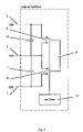
- FIG. 1 is an overall circuit arrangement according to the invention
- FIGS. 2 and 3 are different embodiments of the midpoint stabilizers.
- the overall circuit organization is shown in FIG. 1 .
- the first sub-circuit 1 of the payload circuitry has a power supply line 2 , which maintains the voltage level of VBB and a ground connection 3 , which is to maintain voltage level VHH.
- the ground connection 3 is also routed to the midpoint stabilizer 4 and functions as power supply line to the further sub-circuit 6 of the payload circuitry.
- This sub-circuit 6 further has a ground connection 7 with the voltage level of GND.
- the midpoint stabilizer 4 ensures that the voltage in the power supply line 3 that connects sub-circuit 1 to sub-circuit 6 remains constant and at the midpoint between the battery supply voltage VBB and the ground level GND.
- Level shifters 8 are mandatory wherever a signal crosses over from the lower partition to the upper partition or vice versa. Depending on the peripheral voltage levels, level-shifters 9 are likely to be required on input and output signals as well.
- FIG. 2 or 3 fits into FIG. 1 as midpoint stabilizer circuit 4 and connects by way of common circuit nodes including the three voltage levels VBB, VHH and GND through lines 2 , 3 and 7 respectively. All implementations share the goal of making the voltages across the two payload circuits 1 and 6 in FIG. 1 the same.
- FIGS. 2 and 3 include no dissipative shunts in their circuits as is otherwise known from the prior art. Instead, they feature extra capacitors that act as buckets for charge transfer.
- FIG. 2 includes one such bucket capacitor 20 that gets rapidly switched back and forth between the upper and lower payload circuit as the two-throw switches 25 and 28 alternate between their two stable positions.
- the bucket capacitor 20 accepts extra charge at the higher of the two voltages (VBB-VHH and VHH-GND) and releases that charge at the lower voltage thereby compensating for any momentary difference in the current drains of the two payload circuits.
- FIG. 3 is more sophisticated in that it includes two such bucket capacitors 21 and 22 and four switches 35 , 36 , 37 and 38 .
- switches 25 and 28 in FIGS. 2 and 35 , 36 , 37 and 38 in FIG. 3 may or may not be implemented with the aid of transistors (field-effect transistor FET or bipolar junction transistor BJT, switches in micromechanical technologies, or any other electrically controlled devices).
Landscapes
- Dc-Dc Converters (AREA)
- Semiconductor Integrated Circuits (AREA)
- Electronic Switches (AREA)
- Metal-Oxide And Bipolar Metal-Oxide Semiconductor Integrated Circuits (AREA)
- Amplifiers (AREA)
- Logic Circuits (AREA)
- Control Of Electrical Variables (AREA)
- Dram (AREA)
Applications Claiming Priority (4)
| Application Number | Priority Date | Filing Date | Title |
|---|---|---|---|
| EP03388028 | 2003-04-30 | ||
| EP03388028.7 | 2003-04-30 | ||
| EP20030388028 EP1473812B1 (de) | 2003-04-30 | 2003-04-30 | Integrierte Schaltung mit niedriger Versorgungsspannung |
| PCT/EP2004/004433 WO2004098016A2 (en) | 2003-04-30 | 2004-04-27 | Low-voltage ic-circuit |
Publications (2)
| Publication Number | Publication Date |
|---|---|
| US20070253235A1 US20070253235A1 (en) | 2007-11-01 |
| US7710192B2 true US7710192B2 (en) | 2010-05-04 |
Family
ID=32981997
Family Applications (1)
| Application Number | Title | Priority Date | Filing Date |
|---|---|---|---|
| US10/554,634 Expired - Fee Related US7710192B2 (en) | 2003-04-30 | 2004-04-27 | Low-voltage IC-circuit |
Country Status (7)
| Country | Link |
|---|---|
| US (1) | US7710192B2 (de) |
| EP (1) | EP1473812B1 (de) |
| AT (1) | ATE332586T1 (de) |
| AU (1) | AU2004234945B2 (de) |
| DE (1) | DE60306621T2 (de) |
| DK (1) | DK1473812T3 (de) |
| WO (1) | WO2004098016A2 (de) |
Cited By (8)
| Publication number | Priority date | Publication date | Assignee | Title |
|---|---|---|---|---|
| US20110115554A1 (en) * | 2009-11-18 | 2011-05-19 | Pelley Perry H | System having multiple voltage tiers and method therefor |
| US20110115550A1 (en) * | 2009-11-18 | 2011-05-19 | Pelley Perry H | System and method for communicating between multiple voltage tiers |
| US8878387B1 (en) * | 2013-05-16 | 2014-11-04 | Micrel, Inc. | Multi-level stack voltage system for integrated circuits |
| US20150168973A1 (en) * | 2013-12-18 | 2015-06-18 | Hashfast LLC | Stacked chips powered from shared voltage sources |
| CN105515368A (zh) * | 2014-10-15 | 2016-04-20 | 联合聚晶股份有限公司 | 多电压驱动电路 |
| US9514264B1 (en) | 2016-01-05 | 2016-12-06 | Bitfury Group Limited | Layouts of transmission gates and related systems and techniques |
| US9645604B1 (en) | 2016-01-05 | 2017-05-09 | Bitfury Group Limited | Circuits and techniques for mesochronous processing |
| US9660627B1 (en) | 2016-01-05 | 2017-05-23 | Bitfury Group Limited | System and techniques for repeating differential signals |
Families Citing this family (3)
| Publication number | Priority date | Publication date | Assignee | Title |
|---|---|---|---|---|
| US7679216B2 (en) * | 2007-07-20 | 2010-03-16 | Infineon Technologies Ag | Power supply scheme for reduced power compensation |
| WO2013109719A1 (en) * | 2012-01-17 | 2013-07-25 | Massachusetts Institute Of Technology | Stacked switched capacitor energy buffer circuit |
| WO2016040917A1 (en) * | 2014-09-13 | 2016-03-17 | The Regents Of The University Of Colorado, A Body Corporate | Stacked switched capacitor energy buffer circuit |
Citations (4)
| Publication number | Priority date | Publication date | Assignee | Title |
|---|---|---|---|---|
| US5781001A (en) * | 1995-10-04 | 1998-07-14 | Sharp Kabushiki Kaisha | Display-driving voltage generating apparatus |
| US6121751A (en) | 1999-03-11 | 2000-09-19 | Lockheed Martin Corporation | Battery charger for charging a stack of multiple lithium ion battery cells |
| US20020084824A1 (en) | 2000-12-28 | 2002-07-04 | International Business Machines Corporation | Stacked voltage rails for low-voltage DC distribution |
| US7329968B2 (en) * | 2003-05-08 | 2008-02-12 | The Trustees Of Columbia University In The City Of New York | Charge-recycling voltage domains for energy-efficient low-voltage operation of digital CMOS circuits |
-
2003
- 2003-04-30 EP EP20030388028 patent/EP1473812B1/de not_active Expired - Lifetime
- 2003-04-30 AT AT03388028T patent/ATE332586T1/de not_active IP Right Cessation
- 2003-04-30 DK DK03388028T patent/DK1473812T3/da active
- 2003-04-30 DE DE2003606621 patent/DE60306621T2/de not_active Expired - Lifetime
-
2004
- 2004-04-27 WO PCT/EP2004/004433 patent/WO2004098016A2/en not_active Ceased
- 2004-04-27 AU AU2004234945A patent/AU2004234945B2/en not_active Ceased
- 2004-04-27 US US10/554,634 patent/US7710192B2/en not_active Expired - Fee Related
Patent Citations (4)
| Publication number | Priority date | Publication date | Assignee | Title |
|---|---|---|---|---|
| US5781001A (en) * | 1995-10-04 | 1998-07-14 | Sharp Kabushiki Kaisha | Display-driving voltage generating apparatus |
| US6121751A (en) | 1999-03-11 | 2000-09-19 | Lockheed Martin Corporation | Battery charger for charging a stack of multiple lithium ion battery cells |
| US20020084824A1 (en) | 2000-12-28 | 2002-07-04 | International Business Machines Corporation | Stacked voltage rails for low-voltage DC distribution |
| US7329968B2 (en) * | 2003-05-08 | 2008-02-12 | The Trustees Of Columbia University In The City Of New York | Charge-recycling voltage domains for energy-efficient low-voltage operation of digital CMOS circuits |
Cited By (12)
| Publication number | Priority date | Publication date | Assignee | Title |
|---|---|---|---|---|
| US20110115554A1 (en) * | 2009-11-18 | 2011-05-19 | Pelley Perry H | System having multiple voltage tiers and method therefor |
| US20110115550A1 (en) * | 2009-11-18 | 2011-05-19 | Pelley Perry H | System and method for communicating between multiple voltage tiers |
| US8169257B2 (en) * | 2009-11-18 | 2012-05-01 | Freescale Semiconductor, Inc. | System and method for communicating between multiple voltage tiers |
| US8476962B2 (en) * | 2009-11-18 | 2013-07-02 | Freescale Semiconductor, Inc. | System having multiple voltage tiers and method therefor |
| US8878387B1 (en) * | 2013-05-16 | 2014-11-04 | Micrel, Inc. | Multi-level stack voltage system for integrated circuits |
| US20150168973A1 (en) * | 2013-12-18 | 2015-06-18 | Hashfast LLC | Stacked chips powered from shared voltage sources |
| CN105515368A (zh) * | 2014-10-15 | 2016-04-20 | 联合聚晶股份有限公司 | 多电压驱动电路 |
| US20160112039A1 (en) * | 2014-10-15 | 2016-04-21 | Integrated Solutions Technology Inc. | Multi-voltage driving circuit |
| CN105515368B (zh) * | 2014-10-15 | 2018-04-06 | 联合聚晶股份有限公司 | 多电压驱动电路 |
| US9514264B1 (en) | 2016-01-05 | 2016-12-06 | Bitfury Group Limited | Layouts of transmission gates and related systems and techniques |
| US9645604B1 (en) | 2016-01-05 | 2017-05-09 | Bitfury Group Limited | Circuits and techniques for mesochronous processing |
| US9660627B1 (en) | 2016-01-05 | 2017-05-23 | Bitfury Group Limited | System and techniques for repeating differential signals |
Also Published As
| Publication number | Publication date |
|---|---|
| DE60306621D1 (de) | 2006-08-17 |
| US20070253235A1 (en) | 2007-11-01 |
| AU2004234945A1 (en) | 2004-11-11 |
| AU2004234945B2 (en) | 2009-08-06 |
| WO2004098016A2 (en) | 2004-11-11 |
| DE60306621T2 (de) | 2007-06-21 |
| ATE332586T1 (de) | 2006-07-15 |
| DK1473812T3 (da) | 2006-10-23 |
| WO2004098016A3 (en) | 2005-01-20 |
| EP1473812B1 (de) | 2006-07-05 |
| EP1473812A1 (de) | 2004-11-03 |
Similar Documents
| Publication | Publication Date | Title |
|---|---|---|
| US11099588B2 (en) | Power combiner and balancer | |
| US7329968B2 (en) | Charge-recycling voltage domains for energy-efficient low-voltage operation of digital CMOS circuits | |
| EP3531237B1 (de) | POWER-INSEL MIT UNABHÄNGIGEN POWER-KENNGRÖßEN FÜR SPEICHER UND LOGIK | |
| US7710192B2 (en) | Low-voltage IC-circuit | |
| KR101598767B1 (ko) | 다중 출력을 갖는 시간 다중화된 커패시터 dc/dc 컨버터 | |
| US8710911B2 (en) | Charge pump circuit and power-supply method for dynamically adjusting output voltage | |
| US6479974B2 (en) | Stacked voltage rails for low-voltage DC distribution | |
| KR101024051B1 (ko) | 분산형 전력 관리 시스템 | |
| US20020027467A1 (en) | Single mode buck/boost regulating charge pump | |
| WO2008083328A2 (en) | Mcu with on-chip boost converter controller | |
| US20080018174A1 (en) | Power control apparatus and method thereof | |
| US6650100B1 (en) | Bootstrap technique for a multiple mode switching regulator | |
| US6084385A (en) | System and method for multi-mode low power voltage regulator | |
| EP3933543A1 (de) | Regler mit geringer abfallspannung für niederspannungsanwendungen | |
| US7679216B2 (en) | Power supply scheme for reduced power compensation | |
| KR102236017B1 (ko) | 복수의 셀이 직렬 연결된 배터리에 사용가능한 전력관리장치 | |
| US20130082669A1 (en) | Scalable multiphase-regulator power-integrated circuit system and method for providing scalable power to the same | |
| US20150077059A1 (en) | Battery monitoring device and battery monitoring system | |
| CN109725673B (zh) | 一种全集成多输出堆叠式低压差线性稳压器 | |
| CN113346716A (zh) | 一种可调节电压的多电源输入智能稳压模块 | |
| EP3009910A1 (de) | Energieversorgungssystem mit mehreren Spannungsschienen verschiedener Spannung, Spannungsüberwachung und Auswahlschaltern zum Verbinden der Lasten mit Spannungsschienen | |
| US11456664B2 (en) | Buck-boost DC-DC converter | |
| US20250015715A1 (en) | Switched-capacitor battery management power supply providing power from portions of a multi-cell battery | |
| CN219285687U (zh) | 一种算力服务器供电系统及算力服务器 | |
| JP2004104903A (ja) | 電源回路 |
Legal Events
| Date | Code | Title | Description |
|---|---|---|---|
| AS | Assignment |
Owner name: BERNAFON AG, SWITZERLAND Free format text: ASSIGNMENT OF ASSIGNORS INTEREST;ASSIGNORS:KAESLIN, HUBERT;FELBER, NORBERT;REEL/FRAME:023752/0566 Effective date: 20051110 Owner name: BERNAFON AG,SWITZERLAND Free format text: ASSIGNMENT OF ASSIGNORS INTEREST;ASSIGNORS:KAESLIN, HUBERT;FELBER, NORBERT;REEL/FRAME:023752/0566 Effective date: 20051110 |
|
| FPAY | Fee payment |
Year of fee payment: 4 |
|
| FEPP | Fee payment procedure |
Free format text: MAINTENANCE FEE REMINDER MAILED (ORIGINAL EVENT CODE: REM.) |
|
| LAPS | Lapse for failure to pay maintenance fees |
Free format text: PATENT EXPIRED FOR FAILURE TO PAY MAINTENANCE FEES (ORIGINAL EVENT CODE: EXP.) |
|
| STCH | Information on status: patent discontinuation |
Free format text: PATENT EXPIRED DUE TO NONPAYMENT OF MAINTENANCE FEES UNDER 37 CFR 1.362 |
|
| FP | Lapsed due to failure to pay maintenance fee |
Effective date: 20180504 |