US8025368B2 - Injection head manufacturing method and injection head - Google Patents
Injection head manufacturing method and injection head Download PDFInfo
- Publication number
- US8025368B2 US8025368B2 US11/869,147 US86914707A US8025368B2 US 8025368 B2 US8025368 B2 US 8025368B2 US 86914707 A US86914707 A US 86914707A US 8025368 B2 US8025368 B2 US 8025368B2
- Authority
- US
- United States
- Prior art keywords
- head chip
- flow path
- ink
- regulating member
- rear side
- Prior art date
- Legal status (The legal status is an assumption and is not a legal conclusion. Google has not performed a legal analysis and makes no representation as to the accuracy of the status listed.)
- Expired - Fee Related, expires
Links
Images




Classifications
-
- B—PERFORMING OPERATIONS; TRANSPORTING
- B41—PRINTING; LINING MACHINES; TYPEWRITERS; STAMPS
- B41J—TYPEWRITERS; SELECTIVE PRINTING MECHANISMS, i.e. MECHANISMS PRINTING OTHERWISE THAN FROM A FORME; CORRECTION OF TYPOGRAPHICAL ERRORS
- B41J2/00—Typewriters or selective printing mechanisms characterised by the printing or marking process for which they are designed
- B41J2/005—Typewriters or selective printing mechanisms characterised by the printing or marking process for which they are designed characterised by bringing liquid or particles selectively into contact with a printing material
- B41J2/01—Ink jet
- B41J2/135—Nozzles
- B41J2/16—Production of nozzles
- B41J2/1607—Production of print heads with piezoelectric elements
- B41J2/1609—Production of print heads with piezoelectric elements of finger type, chamber walls consisting integrally of piezoelectric material
-
- B—PERFORMING OPERATIONS; TRANSPORTING
- B41—PRINTING; LINING MACHINES; TYPEWRITERS; STAMPS
- B41J—TYPEWRITERS; SELECTIVE PRINTING MECHANISMS, i.e. MECHANISMS PRINTING OTHERWISE THAN FROM A FORME; CORRECTION OF TYPOGRAPHICAL ERRORS
- B41J2/00—Typewriters or selective printing mechanisms characterised by the printing or marking process for which they are designed
- B41J2/005—Typewriters or selective printing mechanisms characterised by the printing or marking process for which they are designed characterised by bringing liquid or particles selectively into contact with a printing material
- B41J2/01—Ink jet
- B41J2/015—Ink jet characterised by the jet generation process
- B41J2/04—Ink jet characterised by the jet generation process generating single droplets or particles on demand
- B41J2/045—Ink jet characterised by the jet generation process generating single droplets or particles on demand by pressure, e.g. electromechanical transducers
- B41J2/055—Devices for absorbing or preventing back-pressure
-
- B—PERFORMING OPERATIONS; TRANSPORTING
- B41—PRINTING; LINING MACHINES; TYPEWRITERS; STAMPS
- B41J—TYPEWRITERS; SELECTIVE PRINTING MECHANISMS, i.e. MECHANISMS PRINTING OTHERWISE THAN FROM A FORME; CORRECTION OF TYPOGRAPHICAL ERRORS
- B41J2/00—Typewriters or selective printing mechanisms characterised by the printing or marking process for which they are designed
- B41J2/005—Typewriters or selective printing mechanisms characterised by the printing or marking process for which they are designed characterised by bringing liquid or particles selectively into contact with a printing material
- B41J2/01—Ink jet
- B41J2/135—Nozzles
- B41J2/14—Structure thereof only for on-demand ink jet heads
- B41J2/14201—Structure of print heads with piezoelectric elements
- B41J2/14209—Structure of print heads with piezoelectric elements of finger type, chamber walls consisting integrally of piezoelectric material
-
- B—PERFORMING OPERATIONS; TRANSPORTING
- B41—PRINTING; LINING MACHINES; TYPEWRITERS; STAMPS
- B41J—TYPEWRITERS; SELECTIVE PRINTING MECHANISMS, i.e. MECHANISMS PRINTING OTHERWISE THAN FROM A FORME; CORRECTION OF TYPOGRAPHICAL ERRORS
- B41J2/00—Typewriters or selective printing mechanisms characterised by the printing or marking process for which they are designed
- B41J2/005—Typewriters or selective printing mechanisms characterised by the printing or marking process for which they are designed characterised by bringing liquid or particles selectively into contact with a printing material
- B41J2/01—Ink jet
- B41J2/135—Nozzles
- B41J2/16—Production of nozzles
- B41J2/1621—Manufacturing processes
- B41J2/1623—Manufacturing processes bonding and adhesion
-
- B—PERFORMING OPERATIONS; TRANSPORTING
- B41—PRINTING; LINING MACHINES; TYPEWRITERS; STAMPS
- B41J—TYPEWRITERS; SELECTIVE PRINTING MECHANISMS, i.e. MECHANISMS PRINTING OTHERWISE THAN FROM A FORME; CORRECTION OF TYPOGRAPHICAL ERRORS
- B41J2/00—Typewriters or selective printing mechanisms characterised by the printing or marking process for which they are designed
- B41J2/005—Typewriters or selective printing mechanisms characterised by the printing or marking process for which they are designed characterised by bringing liquid or particles selectively into contact with a printing material
- B41J2/01—Ink jet
- B41J2/135—Nozzles
- B41J2/16—Production of nozzles
- B41J2/1621—Manufacturing processes
- B41J2/1631—Manufacturing processes photolithography
-
- B—PERFORMING OPERATIONS; TRANSPORTING
- B41—PRINTING; LINING MACHINES; TYPEWRITERS; STAMPS
- B41J—TYPEWRITERS; SELECTIVE PRINTING MECHANISMS, i.e. MECHANISMS PRINTING OTHERWISE THAN FROM A FORME; CORRECTION OF TYPOGRAPHICAL ERRORS
- B41J2/00—Typewriters or selective printing mechanisms characterised by the printing or marking process for which they are designed
- B41J2/005—Typewriters or selective printing mechanisms characterised by the printing or marking process for which they are designed characterised by bringing liquid or particles selectively into contact with a printing material
- B41J2/01—Ink jet
- B41J2/135—Nozzles
- B41J2/16—Production of nozzles
- B41J2/1621—Manufacturing processes
- B41J2/164—Manufacturing processes thin film formation
- B41J2/1642—Manufacturing processes thin film formation thin film formation by CVD [chemical vapor deposition]
-
- B—PERFORMING OPERATIONS; TRANSPORTING
- B41—PRINTING; LINING MACHINES; TYPEWRITERS; STAMPS
- B41J—TYPEWRITERS; SELECTIVE PRINTING MECHANISMS, i.e. MECHANISMS PRINTING OTHERWISE THAN FROM A FORME; CORRECTION OF TYPOGRAPHICAL ERRORS
- B41J2/00—Typewriters or selective printing mechanisms characterised by the printing or marking process for which they are designed
- B41J2/005—Typewriters or selective printing mechanisms characterised by the printing or marking process for which they are designed characterised by bringing liquid or particles selectively into contact with a printing material
- B41J2/01—Ink jet
- B41J2/135—Nozzles
- B41J2/16—Production of nozzles
- B41J2/1621—Manufacturing processes
- B41J2/164—Manufacturing processes thin film formation
- B41J2/1646—Manufacturing processes thin film formation thin film formation by sputtering
-
- B—PERFORMING OPERATIONS; TRANSPORTING
- B41—PRINTING; LINING MACHINES; TYPEWRITERS; STAMPS
- B41J—TYPEWRITERS; SELECTIVE PRINTING MECHANISMS, i.e. MECHANISMS PRINTING OTHERWISE THAN FROM A FORME; CORRECTION OF TYPOGRAPHICAL ERRORS
- B41J2/00—Typewriters or selective printing mechanisms characterised by the printing or marking process for which they are designed
- B41J2/005—Typewriters or selective printing mechanisms characterised by the printing or marking process for which they are designed characterised by bringing liquid or particles selectively into contact with a printing material
- B41J2/01—Ink jet
- B41J2/135—Nozzles
- B41J2/14—Structure thereof only for on-demand ink jet heads
- B41J2002/14491—Electrical connection
-
- Y—GENERAL TAGGING OF NEW TECHNOLOGICAL DEVELOPMENTS; GENERAL TAGGING OF CROSS-SECTIONAL TECHNOLOGIES SPANNING OVER SEVERAL SECTIONS OF THE IPC; TECHNICAL SUBJECTS COVERED BY FORMER USPC CROSS-REFERENCE ART COLLECTIONS [XRACs] AND DIGESTS
- Y10—TECHNICAL SUBJECTS COVERED BY FORMER USPC
- Y10T—TECHNICAL SUBJECTS COVERED BY FORMER US CLASSIFICATION
- Y10T29/00—Metal working
- Y10T29/49—Method of mechanical manufacture
- Y10T29/49401—Fluid pattern dispersing device making, e.g., ink jet
Definitions
- the present invention relates to an injection head manufacturing method and an injection head, particularly to a method of manufacturing an injection head wherein a flow path regulating member for regulating the flow path of ink into the channel is arranged on the rear side of the head chip, and the injection head manufactured thereby.
- the conventional art has provided a share mode type injection head wherein voltage is applied to the electrode formed on a drive wall which is separating the channel so that shear deformation, is caused at the drive wall and the ink inside the channel is emitted from the nozzle using the pressure generated inside the channel at this time.
- a share mode type injection head an injection head provided with the so-called harmonica type head chip is known, wherein the drive walls made up of piezoelectric elements and the channels are arranged alternately, and a channel aperture is arranged on each of the front side and rear side (Patent Document 1, 2).
- ink is supplied into each channel from the rear side of the head chip. Accordingly, an ink manifold is connected to the rear side of the head chip, and the ink stored in this ink manifold is supplied to each channel.
- the rear side of such a head chip is provided with a flow path regulating member for regulating the flow of ink into the channel by reducing the area of the aperture on the channel inlet side.
- FIG. 15 is a rear side view of the head chip 600 connected with a flow path regulating member 500 .
- This drawing illustrates a harmonica type head chip 600 wherein the air channels 601 that do not emit ink and the ink channels 602 that emit ink are arranged alternately.
- the flow path regulating member 500 utilizes a plastic film such as a sheet of polyimide having the size capable of covering almost all the surfaces on the rear side of the head chip 600 .
- This film is bonded using an adhesive as an epoxy adhesive.
- an ink inlet 501 is formed so as to conform to each ink channel 602 , thereby reducing the area of the aperture on the rear side (on the side supplied with ink) of each ink channel 602 .
- the ink inlet 501 is provided, for example, by laser processing in such a way as to have a diameter smaller than that of the aperture on the rear side of the ink channel 602 .
- the area of the aperture on the rear side of the ink channel is reduced by the flow path regulating member 500 , whereby easy control of the ink meniscus in the nozzle is ensured and high-speed drive is enabled.
- this arrangement provides the advantage of enhancing the drive characteristics.
- the ink inlets of the flow path regulating member are arranged so as to correspond to all the channels.
- Patent Document 1 Unexamined Japanese Patent Application Publication No. 2004-90374
- Patent Document 2 Unexamined Japanese Patent Application Publication No. 2006-35454
- the coated adhesive may ooze from the ink inlet.
- the ink inlet is formed by laser processing after the flow path regulating member has been connected to the rear side of the head chip.
- this requires complication positioning work, for example, by use of a microscope, for the purpose of ensuring that each ink inlet will conform to the position of each ink channel, with the result that workability is deteriorated.
- the ink inlet having a smaller area than that of the aperture on the rear side of the channel is formed approximately at the center of the aperture in the conventional flow path regulating member.
- the object of the present invention is to provide an injection head manufacturing method capable of ensuring that a flow path regulating member is formed on the rear side of the harmonica type head chip without using an adhesive, wherein there is no concern for possible channel clogging.
- Another object of the present invention is to provide an injection head containing a flow path regulating member on the rear side of the harmonica type head chip wherein there is no concern for possible channel being clogged by adhesive.
- a further object of the present invention is to provide an injection head manufacturing method capable of ensuring that a flow path regulating member is formed on the rear side of the harmonica type head chip without having to use adhesive, wherein this injection head is characterized by freedom from a concern for possible channel clogging, and efficient removal of the bubble remaining in the channel, without bubbles being formed easily.
- a still further object of the present invention is to provide an injection head characterized by a flow path regulating member being formed on the rear side of the harmonica type head chip, freedom from a concern for possible channel being clogged by adhesive, and efficient removal of the bubble remaining in the channel, without bubbles being formed easily.
- An inkjet head including: a head chip wherein channels and drive walls configured with piezoelectric elements are arranged alternatively, aperture of each channel are arranged respectively at a front surface and a rear surface of the head chip, and a drive electrode formed in each channel; and a flow path regulating member arranged at the rear surface of the head chip to regulate ink flow into the channel, wherein shear deformation is caused at the drive wall by applying a voltage so that ink in the channel is emitted; wherein the flow path regulation member is formed by a photosensitive film which is adhered by heat and pressure onto the rear surface of the head chip without using adhesives.
- FIG. 1 is a perspective view showing the head chip portion of the injection head as a first embodiment as viewed from the rear side;
- FIG. 2( a ) is a cross sectional view of the injection head of FIG. 1 , with FIG. 2( b ) being a cross sectional view of an air channel;
- FIGS. 3( a ) through ( e ) are explanatory diagrams representing the head chip manufacturing process
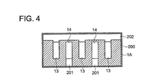
- FIG. 4 is an explanatory diagram representing the head chip manufacturing process
- FIG. 5 is a diagram representing the flow path regulating member manufacturing process, wherein (a) is a cross sectional view of the head chip, and (b) is a rear side view of the head chip;
- FIG. 6 is a diagram representing the flow path regulating member manufacturing process, wherein (a) is a cross sectional view of the head chip, and (b) is a rear side view of the head chip;
- FIG. 7 is a diagram showing the head chip manufacturing process
- FIG. 8 is a cross sectional view representing an example of the injection head
- FIG. 9 is a perspective view showing the head chip portion of the injection head as a second embodiment as viewed from the rear side;
- FIG. 10( a ) is a cross sectional view of the injection head of FIG. 9 , with FIG. 10( b ) being a cross sectional view of an air channel;
- FIG. 11 is a diagram representing the flow path regulating member manufacturing process, wherein (a) is a cross sectional view of the head chip, and (b) is a rear side view of the head chip;
- FIG. 12 is a diagram representing the flow path regulating member manufacturing process, wherein (a) is a cross sectional view of the head chip, and (b) is a rear side view of the head chip;
- FIG. 13 is a cross sectional view showing the head chip portion when the injection head is arranged in a slanting direction;
- FIG. 14 is a rear side view of the head chip portion of the injection head as a third embodiment.
- FIG. 15 is a rear side view of the head chip provided with a conventional flow path regulating member.
- FIG. 1 is a perspective view showing the head chip portion of the injection head as a first embodiment as viewed from the rear side;
- the reference numeral 1 A denotes a head chip and 2 indicates a nozzle plate connected with the front side of the head chip 1 A.
- the surface on the side wherein ink is emitted from the head chip is referred to as the “front side” and the surface opposite thereto is called the “rear side”.
- the outer surfaces on the upper and lower portions in the drawing, sandwiching the channel juxtaposed in the head chip, are called the “upper side” and “lower side”, respectively.
- the drive walls 11 made up of piezoelectric elements, and channels 12 and 13 are arranged alternately on the head chip 1 A.
- five channels 12 and 13 are illustrated by way of an example, without the number of the channels 12 and 13 being restricted thereto.
- the head chip 1 A is an independent channel type head chip wherein channels that emit ink (referred to as “ink channels” in some cases) 12 and the channels that do not emit ink (referred to as “air channels” in some cases) 13 are arranged alternately.
- Each of the channels 12 and 13 is configured in such a way that the walls on both sides rise almost vertical with respect to the upper side and lower side of the head chip 1 A are parallel to each other.
- FIG. 2( a ) is a cross sectional view of the injection head 12 of FIG. 1
- FIG. 2( b ) is a cross sectional view of an air channel 13 .
- each of the channels 12 and 13 and the apertures 122 and 132 on the rear side are arranged face to face with each other on the front side and rear side of the head chip 1 A.
- Each of the channels 12 and 13 is designed in a straight form with a very small change in size and shape along the length from the apertures 122 and 132 on the rear side to the apertures 121 and 131 on the front side.
- a drive electrode 14 made up of Ni, Co, Cu, Al and others is formed in a closely linked configuration on the inner surface of each of the channels 12 and 13 .
- connection electrodes 15 electrically connected with the drive electrode 14 in each of the ink channels 12 are formed by being separately pulled out downward in the drawing.
- One common electrode 16 electrically connected with all of the drive electrodes 14 inside each of the air channels 13 is formed by being pulled out upward in the drawing, in the direction opposite to the connection electrode 15 .
- the piezoelectric element substrate 101 made up of polarized PZTs is connected to one substrate 100 using an epoxy based adhesive, and a photosensitive resin film 102 is bonded on the surface of the piezoelectric element substrate 101 ( FIG. 3( a )).
- a plurality of parallel grooves 103 are ground using a dicing blade and others.
- Each of the grooves 103 is ground from one end of the piezoelectric element substrate 101 to the other end at such a predetermined depth as to almost reach the substrate 100 .
- This arrangement provides a straight form with a very small change in size and shape along the length ( FIG. 3( b )).
- electrode forming metals such as Ni, Co, Cu, Al and others are applied by sputtering method, vapor deposition method or other means, so that a metallic membrane 104 is formed on the upper side of the resin film 102 having been left ungrounded, and on the inner surface of each groove 103 ( FIG. 3( c )).
- the head substrate 106 having been produced is cut in the direction perpendicular to the length of the groove 103 , whereby a plurality of harmonica type head chips 1 A are produced.
- the grooves 103 are formed into the channels 12 and 13 , and the metallic membrane 104 in each groove 103 is formed into a drive electrode 14 .
- the drive wall 11 is created between the adjacent grooves 103 .
- the width between the cut lines C, C . . . determines the drive length (L) of the ink channel 12 of the head chips 1 A, 1 A . . . produced separately, and is determined adequately in response to this drive length ( FIG. 3( e )).
- the rear side of the head chip 1 A having been obtained is provided with a photosensitive resin film 200 wherein an opening 201 for forming a connection electrode 15 , and an opening 202 for forming a common electrode 16 are formed by exposure and development. From the side of the photosensitive resin film 200 , such electrode metals as Ni, Co, Cu and Al are applied so that the connection electrode 15 and common electrode 16 are formed inside each of the openings 201 and 202 on a selective basis ( FIG. 4 ).
- the openings 201 and 202 are preferably provided over all the surfaces of the channels 12 and 13 when consideration is given to the working efficiency in the development and rinsing processes of the photosensitive resin film 200 . This preferred arrangement ensures easy removal of the developing solution and rinsing water from the channels 12 and 13 .
- a nozzle plate 2 is connected to the front side of the head chip 1 A in the aforementioned manner as shown in FIG. 1 and FIG. 2 .
- the nozzle plate 2 is provided with a nozzle 21 only at the position conforming to the ink channel 12 .
- the aperture 131 on the front side of the air channel 13 which does not emit ink is blocked by the nozzle plate 2 .
- Such a harmonica type head chip 1 A is provided with the flow path regulating members 3 for regulating the flow path independently for each air channel 13 to ensure that ink is supplied from the rear side and that ink is not supplied to the aperture 132 on the rear side of each air channel 13 . Thus, this aperture 132 is completely blocked.
- the flow path regulating member 3 is preferably formed on the rear side of the head chip 1 A before the nozzle plate 2 is connected. Accordingly, as shown in FIGS. 5( a ) and ( b ), a photosensitive resin film 300 is bonded by heat and pressure on the head chip 1 A wherein the connection electrode 15 and common electrode 16 have been formed on the rear side, over the entire surface of the rear side using a laminator apparatus, without using an adhesive. In this case, both the apertures 122 and 132 on the rear side of each of the ink channel 12 and air channel 13 are completely blocked by the photosensitive resin film 300 .
- photosensitive dry film Various forms of commercially available photosensitive resin films (called the photosensitive dry film) can be used as the photosensitive resin film 300 .
- the photosensitive cover ray film “Raytec” by Hitachi Chemical Co., Ltd. can be mentioned as an example.
- the FR-5425 having a thickness of 25 ⁇ m was used, and was bonded on the rear side of the head chip 1 by heat and pressure using a laminator apparatus.
- the thickness of the photosensitive resin film 300 namely, the film thickness of the flow path regulating member 3 is preferably in the range of 10 through 100 ⁇ m from the viewpoint of film strength and resolution in the exposure and development processes.
- the photo mask 400 is a rectangular opening 401 having an aperture area a slightly greater than that of the aperture 132 on the rear side of each air channel 13 of the head chip 1 A, so that light can pass through only this opening 401 .
- the photosensitive resin film 300 around each air channel 13 to which light is applied is exposed to light.
- An exposure apparatus is used to position the photo mask 400 with respect to the rear side of the head chip 1 A. This positioning can be achieved to an accuracy of several microns. This accuracy cannot possibly be achieved by the conventional way of bonding a plate having an open ink inlet as a flow path regulating member.
- the ultraviolet ray was applied from the side of the photo mask 400 .
- the amount of exposure was 100 mJ/cm 2 .
- the photo mask 400 was removed, and the material was developed, washed and dried by 1% Na 2 CO 3 using a developer having a temperature of 30 degrees Celsius.
- the flow path regulating members 3 , 3 . . . made up of photosensitive resin films are independently formed on the rear side of the head chip 1 A so that the aperture 132 on the rear side of each air channel 13 is blocked, as shown in FIGS. 6( a ) and ( b ).
- the entire surface is preferably exposed to 1 J/cm 2 ultraviolet ray from the side of this flow path regulating member 3 , and the flow path regulating member 3 is preferably baked at 160 degrees Celsius for one hour. Further, the reaction of the photosensitive resin film proceeds to produce a film characterized by excellent durability.
- Various types of dry films such as dry film resists FRA 063 and FX900 by Du Pont Co., Ltd., and the photosensitive polyimide film by Mitsui Petrochemical Industries, Ltd. can be used as a photosensitive resin film. It is also possible to utilize a photosensitive cover ray film for printed wiring board. As will be described later, especially when parylene is used as a protective film, the photosensitive resin film is not required to have resistance to ink in particular. Accordingly, various forms of photosensitive resin films can be employed.
- the flow path regulating member 3 is bonded by heat and pressure using the photosensitive resin film 300 , without using an adhesive.
- the photo masks 400 with an opening 401 having a predetermined pattern are stacked one on top of the other, whereby the flow path regulating member 3 is formed by exposure and development.
- the drive electrode 14 in the ink channel 12 is brought in direct contact with ink.
- a protect film must be coated on the surface of the drive electrode 14 .
- the flow path regulating member 3 is also brought in direct contact.
- parylene film 17 A film made of paraxylylene and derivatives thereof (hereinafter referred to as “parylene film 17 ) is preferably used as a protective film 17 for coating.
- the parylene film 17 is a resin film made of a polyparaxylylene resin and/or its derivative resin. It is formed by the Chemical Vapor Deposition: CVD method) wherein the solid diparaxylylene dimer or its derivative is a source of vapor deposition.
- CVD method Chemical Vapor Deposition
- the paraxylylene radical produced by vaporization and thermal decomposition of the diparaxylylene dimer is adsorbed on the surfaced of the head chip 1 A, and a film is formed by polymerization.
- parylene films 17 There are various types of parylene films 17 . In response to required performances, various forms of parylene films, or a multi-layer parylene film made up of a plurality of these parylene films laminated one on top of the other can be used as a desired parylene film 17 .
- Such a parylene film 17 preferably has a thickness of 1 ⁇ m through 10 ⁇ m.
- the parylene film 17 permeates fine areas to form a film.
- the drive electrode 14 as well as the flow path regulating member 3 are protected against ink since both the inner surface facing the interior of the air channel 13 and the outer surface exposed to the rear side of the head chip 1 A are coated with the parylene film 17 .
- the flow path regulating member 3 is protected on both sides by the formation of this parylene film 17 , with the result that the durability is greatly improved. Generally, due to insufficient adhesive strength, the surface of the photosensitive resin film must be roughened to enhance adhesive strength in some cases. Since the parylene film 17 sufficient adhesive strength when bonded with the substrate, the flow path regulating member 3 is pushed from both sides by the parylene film 17 , and the flow path regulating member 3 having insufficient adhesive strength can also be used for a long time.
- the parylene film 17 per se does not dissolve, and continues to be present on both surfaces of the flow path regulating member 3 . Thus, it does not lose the function as the flow path regulating member, and its reliability is maintained for a long period of time.
- the flow path regulating member 3 is formed independently for each air channel 13 .
- the adverse effect of a pin-hole having occurred to the parylene film 17 is restricted to the flow path regulating member 3 alone, so that the flow path regulating member 3 of other air channels 13 is not affected.
- This arrangement provides an advantage that the damage is kept to a minimum.
- the flow path regulating member 3 is formed independently for each air channel 13 . This arrangement ensures that other flow path regulating members 3 are not affected, even if separation or other defects have occurred to any of the flow path regulating members 3 .
- the nozzle plate 2 is connected to the front side of the head chip 1 A, as shown in FIG. 7 .
- the wiring board 4 for example, as shown in FIG. 8 is connected to the rear side of the head chip 1 A, whereby the connection electrode 15 and common electrode 16 formed on the rear side of the heed chip 1 A are electrically connected with the drive circuit (not illustrated).
- FIG. 8 is a cross sectional view wherein the head chip 1 A connected with the wiring board 4 is cut at the air channel 13 .
- the wiring board 4 is formed of a plate-formed substrate which is made up of a ceramic material such as a nonpolarizable PZT, AIN-BN and AIN. Plastic and glass of low thermal expansion can also be used. Further, the same substrate material as that of the piezoelectric element substrate used in the head chip 1 can be used for depolarization. Further, to reduce the distortion of the head chip 1 resulting from the difference in coefficient of thermal expansion, the material is preferably selected so that the difference in the coefficient of thermal expansion from the head chip 1 A will be kept within ⁇ 1 ppm.
- the number of the materials constituting the wiring board 4 is not restricted to one. Several sheets of thin plate-formed substrate materials can be laminated to get a desired thickness.
- the wiring board 4 extends in the direction perpendicular to the direction of a row of the channels of the head chip 1 A (in the vertical direction in FIG. 8 ).
- the overhangs 41 a and 41 b that hangs substantially over the upper side and lower side of the head chip 1 A are provided.
- one concave portion 42 extending across the width (in the direction of channel row) is formed on one surface of the wiring board 4 connected with the rear side of the head chip 1 A.
- This concave portion 42 is provided with a groove large enough to cover the apertures 122 and 132 on the rear side of all the channels 12 and 13 in the direction of the channel row of the head chip 1 A.
- the height of the concave portion 42 in the vertical direction of the drawing is greater than that of each of the channels 12 and 13 , and is smaller than the thickness perpendicular to the direction of the channel row of the head chip 1 A.
- the apertures 122 and 132 on the rear side of each of the channels 12 and 13 faces inside the concave portion 42 .
- the flow path regulating member 3 is built in this concave portion 42 .
- the wiring board 4 is connected to a very narrow area on the rear side of the head chip 1 A where the flow path regulating member 3 is not provided. This area is very close to each of the channels 12 and 13 (e.g., the distance is 0 through 200 ⁇ m). This requires a very difficult and high-precision positioning work when one plate-formed flow path regulating member is connected in the conventional manner.
- the flow path regulating member 3 is formed by exposure and development of the photosensitive resin film. This arrangement ensures high-precision positioning, as described above, and allows the channels 12 and 13 to be easily formed in a very close position.
- One of the overhangs 41 a of the wiring board 4 is provided with the wired electrodes 43 (not illustrated in FIG. 8 ) each having the same number and same pitch as those of the connection electrodes 15 (not illustrated in FIG. 8 ) formed on the rear side of the head chip 1 A.
- the other overhang 41 b is provided with a wired electrode 44 for connection with the common electrode 16 formed on the rear side of the head chip 1 A.
- the wiring board 4 is connected to the rear side of the head chip 1 A by an anisotropic conductive film or the like so that each of the wired electrodes 43 will be electrically connected with each of the connection electrodes 15 , and the wired electrode 44 is electrically connected with the common electrode 16 .
- ink can be supplied to the concave portion 42 serving as a common ink chamber from both ends of the concave portion 42 or one of the ends. It is also possible to form an opening 45 leading from the bottom of the concave portion 42 to the surface opposite to the surface for connection with the head chip 1 A, and to further connect a box-shaped ink manifold 46 capable of storing the ink in the amount greater than that of the concave portion 42 , as shown in FIG. 8 .
- the aforementioned parylene film 17 is formed preferably before the nozzle plate 2 is connected to the head chip 1 A after the wiring board 4 has been connected to the head chip 1 A.
- This arrangement ensures electrical connection between each of the connection electrodes 15 and common electrodes 16 , and each of the wired electrodes 43 and 44 , and allows a protective film to be formed on the surface of the wired electrodes 43 and 44 facing the concave portion 42 of the wiring board 4 which will be brought in direct contact with ink.
- FIG. 9 is a perspective view of the head chip of the injection head of the second embodiment, as viewed from the rear side.
- FIG. 10( a ) is a cross sectional view showing the ink channel 12 of the injection head of FIG. 9
- FIG. 10( b ) is a cross sectional view of the air channel 13 .
- FIGS. 1 and 2 are assigned to the same components, which will not be described in details to avoid duplication. Further, the method of manufacturing this head chip 1 B is the same as that of FIG. 3 and FIG. 4 .
- each ink channel 12 is provided with a flow path regulating member 32 independently so as to reduce the area of the aperture 122 on the rear side thereof.
- the direction of width in the direction of the channel row is slightly greater than the width ink channel 12 , and the vertical direction perpendicular to the direction of width is smaller than the height of the ink channel 12 . Accordingly, the aperture area is reduced by the flow path regulating member 32 to ensure that only the top end and bottom end of each of the apertures 122 on the rear side of the ink channel 12 will open.
- This flow path regulating member 32 is preferably formed on the rear side of the head chip 1 B before the nozzle plate 2 is connected. Accordingly, as shown in FIGS. 11( a ) and ( b ), the photosensitive resin film 300 is bonded by heat and pressure on all surfaces of the rear side of the head chip 1 B, using a laminator apparatus, without using an adhesive, wherein the connection electrode 15 and common electrode 16 have already been formed on the rear side of this head chip 1 B. In this case, both the apertures 122 and 132 on the rear side of each of the air channel 13 and the ink channels 12 is completely blocked by the photosensitive resin film 300 , similarly to the case of FIG. 5 .
- this photosensitive resin film 300 namely, the thickness between flow path regulating members 31 and 32 can be made the same as that of the aforementioned flow path regulating member 3 .
- this photo mask 400 has an rectangular opening 402 having an aperture area which is slightly smaller than that of the aperture 122 on the rear side of each of the ink channels 12 and which does not lead to the top end and bottom end of the aperture 122 .
- Light is allowed to pass through these openings 401 and 402 alone. Light is applied by using this photo mask 400 , whereby light is applied only to the photosensitive resin film 300 around each of the ink channels 12 and each of the air channels 13 exposed to light.
- ultraviolet ray is applied from the side of the photo mask 400 for exposure, similarly to the case of FIG. 5 . Then the photo mask 400 is removed, and the material is subjected to the processes of development, rinsing, drying, post-exposure and baking.
- a flow path regulating member 31 made up of a photosensitive resin film is independently formed on the rear side of the head chip 1 B so as to block the aperture 132 on the rear side of each of the air channels 13 .
- the flow path regulating member 32 made up of the photosensitive resin film is independently formed so as to reduce the area of the aperture 122 on the rear side of each of the ink channels 12 .
- this flow path regulating member 32 is formed by exposure and development are performed through lamination of the photo masks 400 with an opening 402 having a predetermined pattern. This arrangement eliminates the possibility of the channel being clogged by adhesive. Further, the member is formed by patterning through exposure and development. This arrangement ensures high-precision reduction in the area of the aperture 122 on the rear side of each of the ink channels 12 .
- a parylene film 17 is preferably formed on all the surfaces of the head chip 1 B, namely, on the surface of each of the drive electrode 14 and the surfaces of the flow path regulating members 31 and 32 , subsequent to connection, similarly to the case of FIG. 7 .
- the area of the aperture 12 on the rear side of each of the ink channels 12 is reduced by the flow path regulating member 32 .
- This arrangement permits an effective reduction in the vibration of the ink meniscus of the nozzle when the head is driven at a high speed, similarly to the conventional case of using the flow path regulating plate with the ink inlet kept open.
- this flow path regulating member 32 is designed in such a way that the top end and bottom end of the aperture 122 of the ink channel 12 are opened to form the apertures 122 a and 122 b .
- the aperture e.g., aperture 122 a
- the aperture which is not blocked by the flow path regulating member 32 is located at the top-most position for the ink channel 12 .
- the bubble b produced in the ink channel 12 is collected to this top-most position and is easily removed from the aperture 122 a to enter the common ink chamber outside the head chip 1 B. Even if there is bubble b inside the common ink chamber, it does not affect injection any more. This eliminates the possibility of any problem being caused by bubble b.
- This aperture 122 is made to open by the flow path regulating member 32 formed so as to reduce the area of the aperture 122 on the rear side of the of each of the ink channels 12 .
- This arrangement provides a head characterized by excellent bubble removing performance and injection reliability.
- the area of the aperture 122 on the rear side after having been narrowed by the flow path regulating member 32 is preferably 1 through 10 times the aperture area on the emission side of the nozzle 21 formed on the nozzle plate 2 , more preferably 2 through 5 times.
- the optimum value is preferably obtained from the result of an injection test. According to the test made by the present inventors, the optimum area of the aperture 122 on the rear side after having been reduced by the flow path regulating member 32 is 2000 ⁇ m 2 for the head chip having a nozzle diameter of 28 ⁇ m (aperture area: 615 ⁇ m 2 ).
- the flow path regulating member 32 was formed in such a way that both the top end and bottom end of the aperture 122 of the ink channel 12 are opened to form apertures 122 a and 122 b , respectively.
- This arrangement allows the bubble b to be removed independently of whether the upper side or lower side of the head chip 1 B is located on the upper position, and does not impose any restriction when the injection head is installed in a slanting direction.
- the flow path regulating member 32 can be formed in such a way that either the top end or bottom end alone in the aperture 122 on the rear side of the ink channel 12 is open. In this case, the injection head is installed in a slanting direction so that the open side of the apertures 122 on the rear side without being blocked by the flow path regulating member 32 is located on the upper position. This arrangement makes it possible to remove the bubble b.
- the first embodiment and the second embodiment use an example of the independent channel type injection head wherein the channels arranged side by side on the head chips 1 A and 1 B were assigned alternately as ink channels 12 and air channels 13 . However, in the head chip, all the channels can be used as ink channels 12 .
- FIG. 14 indicated the rear side of the head chip 1 C in the third embodiment when all the channels are used as ink channels 12 .
- the same reference numerals in FIGS. 1 and 2 indicate the same structure, and will not be described in details.
- the manufacturing methods of this head chip 1 C in FIG. 3 and FIG. 4 are the same. In this case as well, the drive electrode 14 is not illustrated.
- a flow path regulating member 32 made up of the photosensitive resin film is formed independently on the aperture 122 on the rear side of each of the ink channels 12 so as to reduce the area of the aperture 122 .
- the area of the aperture 122 on the rear side of each of the ink channels 12 is reduced by the flow path regulating member 32 so that the top end and bottom end are open.
- the flow path regulating member 32 can be formed of one flow path regulating member so as to reduce the area of the apertures 122 on the rear sides of all the ink channels 12 . In this case as well, as illustrated, if it is formed independently for each ink channel 12 , other ink channels 12 are not affected by the problems of any of the flow path regulating members 32 .
- the flow path regulating member 32 can be formed in such a way that either the top end or bottom end alone in the aperture 122 on the rear side of the ink channel 12 is open.
- the head chips 1 A, 1 B and 1 C constituting the injection head each have only one channel row.
- a plurality of channel rows can be used.
- the flow path regulating members 3 , 31 and 32 can be applied in the same manner.
- the aforementioned embodiment provides an injection head manufacturing method wherein a flow path regulating member is formed on the rear side of the harmonica type head chip without using an adhesive, and there is no possibility of the channel being clogged.
- the aforementioned embodiment also provides an injection head manufacturing method wherein bubbles are easily removed from the channel so that bubbles hardly remain inside.
- the aforementioned embodiment also provides an injection head having a flow path regulating member on the rear side of the harmonica type head chip, without any possible of the channel being clogged by adhesive.
- the aforementioned embodiment also provides an injection head wherein bubbles are easily removed from the channel so that bubbles hardly remain inside.
Landscapes
- Engineering & Computer Science (AREA)
- Manufacturing & Machinery (AREA)
- Particle Formation And Scattering Control In Inkjet Printers (AREA)
- Fuel-Injection Apparatus (AREA)
- Injection Moulding Of Plastics Or The Like (AREA)
Priority Applications (1)
| Application Number | Priority Date | Filing Date | Title |
|---|---|---|---|
| US13/159,844 US8403462B2 (en) | 2006-10-13 | 2011-06-14 | Injection head manufacturing method and injection head |
Applications Claiming Priority (2)
| Application Number | Priority Date | Filing Date | Title |
|---|---|---|---|
| JP2006-280645 | 2006-10-13 | ||
| JP2006280645A JP2008094036A (ja) | 2006-10-13 | 2006-10-13 | インクジェットヘッドの製造方法及びインクジェットヘッド |
Related Child Applications (1)
| Application Number | Title | Priority Date | Filing Date |
|---|---|---|---|
| US13/159,844 Division US8403462B2 (en) | 2006-10-13 | 2011-06-14 | Injection head manufacturing method and injection head |
Publications (2)
| Publication Number | Publication Date |
|---|---|
| US20080088678A1 US20080088678A1 (en) | 2008-04-17 |
| US8025368B2 true US8025368B2 (en) | 2011-09-27 |
Family
ID=38947929
Family Applications (2)
| Application Number | Title | Priority Date | Filing Date |
|---|---|---|---|
| US11/869,147 Expired - Fee Related US8025368B2 (en) | 2006-10-13 | 2007-10-09 | Injection head manufacturing method and injection head |
| US13/159,844 Expired - Fee Related US8403462B2 (en) | 2006-10-13 | 2011-06-14 | Injection head manufacturing method and injection head |
Family Applications After (1)
| Application Number | Title | Priority Date | Filing Date |
|---|---|---|---|
| US13/159,844 Expired - Fee Related US8403462B2 (en) | 2006-10-13 | 2011-06-14 | Injection head manufacturing method and injection head |
Country Status (5)
| Country | Link |
|---|---|
| US (2) | US8025368B2 (de) |
| EP (1) | EP1911591B1 (de) |
| JP (1) | JP2008094036A (de) |
| AT (1) | ATE430033T1 (de) |
| DE (1) | DE602007001012D1 (de) |
Cited By (5)
| Publication number | Priority date | Publication date | Assignee | Title |
|---|---|---|---|---|
| US20130027493A1 (en) * | 2011-07-28 | 2013-01-31 | Kyocera Document Solutions Inc. | Inkjet recording apparatus |
| US11845280B2 (en) | 2021-08-26 | 2023-12-19 | Toshiba Tec Kabushiki Kaisha | Liquid ejecting head and liquid ejecting device |
| US12036794B2 (en) | 2021-09-24 | 2024-07-16 | Toshiba Tec Kabushiki Kaisha | Liquid ejection head |
| US12049081B2 (en) | 2021-08-26 | 2024-07-30 | Toshiba Tec Kabushiki Kaisha | Liquid ejecting head and method of manufacturing liquid ejecting head |
| US20240278563A1 (en) * | 2023-02-22 | 2024-08-22 | Toshiba Tec Kabushiki Kaisha | Liquid ejection head |
Families Citing this family (7)
| Publication number | Priority date | Publication date | Assignee | Title |
|---|---|---|---|---|
| KR101063450B1 (ko) * | 2009-01-21 | 2011-09-08 | 삼성전기주식회사 | 잉크젯 헤드 제조방법 |
| KR102011450B1 (ko) * | 2012-06-21 | 2019-08-19 | 삼성디스플레이 주식회사 | 잉크젯 프린트 헤드 및 이의 제조 방법 |
| JP5775045B2 (ja) * | 2012-09-24 | 2015-09-09 | 株式会社東芝 | インクジェットヘッド |
| JP6155370B2 (ja) * | 2016-07-13 | 2017-06-28 | 株式会社東芝 | インクジェットヘッド |
| JP7010067B2 (ja) * | 2018-03-07 | 2022-01-26 | コニカミノルタ株式会社 | インクジェットヘッドの製造方法 |
| JP7146521B2 (ja) * | 2018-08-09 | 2022-10-04 | 東芝テック株式会社 | インクジェットヘッド、インクジェット装置、及びインクジェットヘッドの製造方法 |
| JP7689066B2 (ja) * | 2021-12-10 | 2025-06-05 | 理想テクノロジーズ株式会社 | 液体吐出ヘッド |
Citations (11)
| Publication number | Priority date | Publication date | Assignee | Title |
|---|---|---|---|---|
| EP0505188A2 (de) | 1991-03-19 | 1992-09-23 | Brother Kogyo Kabushiki Kaisha | Piezoelektrische Vorrichtung zur Erzeugung eines Strahles aus Tintentröpfchen |
| US5736278A (en) * | 1995-06-20 | 1998-04-07 | Canon Kabushiki Kaisha | Color filter having light screening resin layer and filter resin layer |
| US20020073544A1 (en) | 2000-12-18 | 2002-06-20 | Konica Corporation | Manufacturing method of ink-jet haead |
| US20030011660A1 (en) | 1998-12-04 | 2003-01-16 | Konica Corporation | Method of manufacturing an ink-jet head |
| JP2004090374A (ja) | 2002-08-30 | 2004-03-25 | Konica Minolta Holdings Inc | インクジェットヘッド |
| US20040130602A1 (en) * | 2002-12-27 | 2004-07-08 | Konica Minolta Holdings, Inc. | Ink jet head |
| US20060017778A1 (en) * | 2004-07-22 | 2006-01-26 | Konica Minolta Holdings, Inc. | Inkjet print head and manufacturing method thereof |
| US7004561B2 (en) * | 2002-04-19 | 2006-02-28 | Sony Corporation | Liquid discharge apparatus, printer head, and method for making liquid discharge apparatus |
| US20060055741A1 (en) * | 2004-09-16 | 2006-03-16 | Konica Minolta Holdings, Inc. | Ink-jet head |
| US20070030316A1 (en) * | 2005-08-02 | 2007-02-08 | Konica Minolta Holdings, Inc. | Inkjet head and method of manufacturing inkjet head |
| US20070070125A1 (en) * | 2005-08-23 | 2007-03-29 | Konica Minolta Holdings, Inc. | Inkjet head and method of manufacturing inkjet head |
Family Cites Families (1)
| Publication number | Priority date | Publication date | Assignee | Title |
|---|---|---|---|---|
| US6895669B2 (en) * | 2002-02-08 | 2005-05-24 | Konica Corporation | Method of manufacturing an ink jet head |
-
2006
- 2006-10-13 JP JP2006280645A patent/JP2008094036A/ja active Pending
-
2007
- 2007-10-09 US US11/869,147 patent/US8025368B2/en not_active Expired - Fee Related
- 2007-10-09 AT AT07254006T patent/ATE430033T1/de not_active IP Right Cessation
- 2007-10-09 DE DE602007001012T patent/DE602007001012D1/de active Active
- 2007-10-09 EP EP07254006A patent/EP1911591B1/de not_active Not-in-force
-
2011
- 2011-06-14 US US13/159,844 patent/US8403462B2/en not_active Expired - Fee Related
Patent Citations (12)
| Publication number | Priority date | Publication date | Assignee | Title |
|---|---|---|---|---|
| EP0505188A2 (de) | 1991-03-19 | 1992-09-23 | Brother Kogyo Kabushiki Kaisha | Piezoelektrische Vorrichtung zur Erzeugung eines Strahles aus Tintentröpfchen |
| US5736278A (en) * | 1995-06-20 | 1998-04-07 | Canon Kabushiki Kaisha | Color filter having light screening resin layer and filter resin layer |
| US20030011660A1 (en) | 1998-12-04 | 2003-01-16 | Konica Corporation | Method of manufacturing an ink-jet head |
| US20020073544A1 (en) | 2000-12-18 | 2002-06-20 | Konica Corporation | Manufacturing method of ink-jet haead |
| US7004561B2 (en) * | 2002-04-19 | 2006-02-28 | Sony Corporation | Liquid discharge apparatus, printer head, and method for making liquid discharge apparatus |
| JP2004090374A (ja) | 2002-08-30 | 2004-03-25 | Konica Minolta Holdings Inc | インクジェットヘッド |
| US20040130602A1 (en) * | 2002-12-27 | 2004-07-08 | Konica Minolta Holdings, Inc. | Ink jet head |
| US20060017778A1 (en) * | 2004-07-22 | 2006-01-26 | Konica Minolta Holdings, Inc. | Inkjet print head and manufacturing method thereof |
| JP2006035454A (ja) | 2004-07-22 | 2006-02-09 | Konica Minolta Holdings Inc | インクジェットヘッドの製造方法 |
| US20060055741A1 (en) * | 2004-09-16 | 2006-03-16 | Konica Minolta Holdings, Inc. | Ink-jet head |
| US20070030316A1 (en) * | 2005-08-02 | 2007-02-08 | Konica Minolta Holdings, Inc. | Inkjet head and method of manufacturing inkjet head |
| US20070070125A1 (en) * | 2005-08-23 | 2007-03-29 | Konica Minolta Holdings, Inc. | Inkjet head and method of manufacturing inkjet head |
Non-Patent Citations (1)
| Title |
|---|
| European Search Report for European Application No. EP07-254006 mailed Feb. 14, 2008. |
Cited By (6)
| Publication number | Priority date | Publication date | Assignee | Title |
|---|---|---|---|---|
| US20130027493A1 (en) * | 2011-07-28 | 2013-01-31 | Kyocera Document Solutions Inc. | Inkjet recording apparatus |
| US9227405B2 (en) * | 2011-07-28 | 2016-01-05 | Kyocera Document Solutions Inc. | Inkjet recording apparatus |
| US11845280B2 (en) | 2021-08-26 | 2023-12-19 | Toshiba Tec Kabushiki Kaisha | Liquid ejecting head and liquid ejecting device |
| US12049081B2 (en) | 2021-08-26 | 2024-07-30 | Toshiba Tec Kabushiki Kaisha | Liquid ejecting head and method of manufacturing liquid ejecting head |
| US12036794B2 (en) | 2021-09-24 | 2024-07-16 | Toshiba Tec Kabushiki Kaisha | Liquid ejection head |
| US20240278563A1 (en) * | 2023-02-22 | 2024-08-22 | Toshiba Tec Kabushiki Kaisha | Liquid ejection head |
Also Published As
| Publication number | Publication date |
|---|---|
| US20080088678A1 (en) | 2008-04-17 |
| ATE430033T1 (de) | 2009-05-15 |
| US8403462B2 (en) | 2013-03-26 |
| US20120154490A1 (en) | 2012-06-21 |
| JP2008094036A (ja) | 2008-04-24 |
| DE602007001012D1 (de) | 2009-06-10 |
| EP1911591A1 (de) | 2008-04-16 |
| EP1911591B1 (de) | 2009-04-29 |
Similar Documents
| Publication | Publication Date | Title |
|---|---|---|
| US8025368B2 (en) | Injection head manufacturing method and injection head | |
| US9315016B2 (en) | Inkjet head and method of manufacturing inkjet head | |
| US7523553B2 (en) | Method of manufacturing ink jet recording head | |
| US7918544B2 (en) | Inkjet head | |
| JP2006035454A (ja) | インクジェットヘッドの製造方法 | |
| US7905581B2 (en) | Inkjet head | |
| JP2021000803A (ja) | 液体吐出ヘッド、液体吐出ヘッドの製造方法及び液体吐出装置 | |
| CN101797839A (zh) | 叠层组件和对准叠层的方法 | |
| US8550601B2 (en) | Use of photoresist material as an interstitial fill for PZT printhead fabrication | |
| JP5062354B2 (ja) | インクジェットヘッドの製造方法 | |
| US9061501B2 (en) | Manufacturing method of liquid ejecting head | |
| EP1911592B1 (de) | Herstellungsverfahren für einen Einspritzkopf und Einspritzkopf | |
| JP2003311984A (ja) | インクジェットヘッドの製造方法 | |
| JP2003311951A (ja) | インクジェットヘッド | |
| JP2007069459A (ja) | インクジェットヘッド | |
| JP4967755B2 (ja) | ヘッドモジュール、液体吐出ヘッド、液体吐出装置、及びヘッドモジュールの製造方法 | |
| JP2008162110A (ja) | インクジェットヘッドおよびインクジェットヘッドの製造方法プ実装用配線基板 | |
| JP4983582B2 (ja) | インクジェットヘッド及びインクジェットヘッドの製造方法 | |
| JP4213268B2 (ja) | インクジェットヘッド | |
| JP5622653B2 (ja) | インクジェットヘッドおよびインクジェットヘッドの製造方法 | |
| JP2006035453A (ja) | インクジェットヘッドの製造方法 | |
| JP2022001407A (ja) | 液体吐出ヘッド、吐出ユニット、液体を吐出する装置、貼り合わせ基板 | |
| JP2013147008A (ja) | インクジェットヘッドの製造方法及びインクジェットヘッド | |
| JP2006167969A (ja) | インクジェット記録ヘッドの製造方法 | |
| JP2007062260A (ja) | ヘッドモジュール、液体吐出ヘッド、液体吐出装置、及びヘッドモジュールの製造方法 |
Legal Events
| Date | Code | Title | Description |
|---|---|---|---|
| AS | Assignment |
Owner name: KONICA MINOLTA IJ TECHNOLOGIES, INC., JAPAN Free format text: ASSIGNMENT OF ASSIGNORS INTEREST;ASSIGNOR:WATANABE, HIDEO;REEL/FRAME:019937/0394 Effective date: 20070926 |
|
| FEPP | Fee payment procedure |
Free format text: PAYOR NUMBER ASSIGNED (ORIGINAL EVENT CODE: ASPN); ENTITY STATUS OF PATENT OWNER: LARGE ENTITY |
|
| ZAAA | Notice of allowance and fees due |
Free format text: ORIGINAL CODE: NOA |
|
| ZAAB | Notice of allowance mailed |
Free format text: ORIGINAL CODE: MN/=. |
|
| STCF | Information on status: patent grant |
Free format text: PATENTED CASE |
|
| FPAY | Fee payment |
Year of fee payment: 4 |
|
| MAFP | Maintenance fee payment |
Free format text: PAYMENT OF MAINTENANCE FEE, 8TH YEAR, LARGE ENTITY (ORIGINAL EVENT CODE: M1552); ENTITY STATUS OF PATENT OWNER: LARGE ENTITY Year of fee payment: 8 |
|
| FEPP | Fee payment procedure |
Free format text: MAINTENANCE FEE REMINDER MAILED (ORIGINAL EVENT CODE: REM.); ENTITY STATUS OF PATENT OWNER: LARGE ENTITY |
|
| LAPS | Lapse for failure to pay maintenance fees |
Free format text: PATENT EXPIRED FOR FAILURE TO PAY MAINTENANCE FEES (ORIGINAL EVENT CODE: EXP.); ENTITY STATUS OF PATENT OWNER: LARGE ENTITY |
|
| STCH | Information on status: patent discontinuation |
Free format text: PATENT EXPIRED DUE TO NONPAYMENT OF MAINTENANCE FEES UNDER 37 CFR 1.362 |
|
| FP | Lapsed due to failure to pay maintenance fee |
Effective date: 20230927 |