US8044708B2 - Reference voltage generator - Google Patents
Reference voltage generator Download PDFInfo
- Publication number
- US8044708B2 US8044708B2 US12/643,277 US64327709A US8044708B2 US 8044708 B2 US8044708 B2 US 8044708B2 US 64327709 A US64327709 A US 64327709A US 8044708 B2 US8044708 B2 US 8044708B2
- Authority
- US
- United States
- Prior art keywords
- output
- voltage
- low
- reference voltage
- pass filter
- Prior art date
- Legal status (The legal status is an assumption and is not a legal conclusion. Google has not performed a legal analysis and makes no representation as to the accuracy of the status listed.)
- Expired - Fee Related, expires
Links
- 238000006243 chemical reaction Methods 0.000 claims description 4
- 239000003990 capacitor Substances 0.000 description 18
- 238000010586 diagram Methods 0.000 description 13
- 244000145845 chattering Species 0.000 description 4
- 230000006641 stabilisation Effects 0.000 description 4
- 238000011105 stabilization Methods 0.000 description 4
- 230000003111 delayed effect Effects 0.000 description 3
- 238000004891 communication Methods 0.000 description 2
- 238000009499 grossing Methods 0.000 description 2
- 239000004065 semiconductor Substances 0.000 description 2
- 230000001413 cellular effect Effects 0.000 description 1
- 238000007796 conventional method Methods 0.000 description 1
- 230000000694 effects Effects 0.000 description 1
- 238000002347 injection Methods 0.000 description 1
- 239000007924 injection Substances 0.000 description 1
- 238000000034 method Methods 0.000 description 1
- 239000000243 solution Substances 0.000 description 1
Images


Classifications
-
- G—PHYSICS
- G05—CONTROLLING; REGULATING
- G05F—SYSTEMS FOR REGULATING ELECTRIC OR MAGNETIC VARIABLES
- G05F3/00—Non-retroactive systems for regulating electric variables by using an uncontrolled element, or an uncontrolled combination of elements, such element or such combination having self-regulating properties
- G05F3/02—Regulating voltage or current
- G05F3/08—Regulating voltage or current wherein the variable is DC
- G05F3/10—Regulating voltage or current wherein the variable is DC using uncontrolled devices with non-linear characteristics
- G05F3/16—Regulating voltage or current wherein the variable is DC using uncontrolled devices with non-linear characteristics being semiconductor devices
-
- G—PHYSICS
- G05—CONTROLLING; REGULATING
- G05F—SYSTEMS FOR REGULATING ELECTRIC OR MAGNETIC VARIABLES
- G05F1/00—Automatic systems in which deviations of an electric quantity from one or more predetermined values are detected at the output of the system and fed back to a device within the system to restore the detected quantity to its predetermined value or values, i.e. retroactive systems
- G05F1/10—Regulating voltage or current
- G05F1/46—Regulating voltage or current wherein the variable actually regulated by the final control device is DC
- G05F1/56—Regulating voltage or current wherein the variable actually regulated by the final control device is DC using semiconductor devices in series with the load as final control devices
Definitions
- the present invention relates to a reference voltage generator, and particularly to an improved configuration in which a capacitor of a low-pass filter for reducing the noise of a reference voltage source is charged rapidly so that an output voltage is stabilized rapidly.
- FIG. 7 shows a circuit according to this first conventional example.
- a low-pass filter 2 composed of a resistor R and a capacitor C is connected to a point A to which a voltage of a reference voltage source 1 is outputted so as to reduce noise in a voltage outputted to a point B.
- a resistance value of the resister R is represented by “R”
- a capacitance value of the capacitor C is represented by “C”.
- the voltage at the point B is amplified by a non-inverting amplifier using an operational amplifier 3 and outputted as an output voltage Vout from an output terminal 5 by an output transistor 4 .
- a time constant RC of the low-pass filter 2 is larger than a time constant of, for example, a transistor constituting the reference voltage source 1 or the operational amplifier 3 . Because of this, after power-on, a considerable time is required for the output voltage Vout to rise logarithmically with the time constant RC until it is stabilized to a steady state.
- FIG. 9 shows waveforms of the output voltage Vout until they are stabilized. The horizontal axis indicates a time and the vertical axis indicates a value of the output voltage Vout. It can be understood that in the case of an output waveform P 1 of the first conventional example, a considerable amount of time is required until the output voltage Vout is stabilized.
- FIG. 8 shows a circuit according to this second conventional example.
- a point B that is an output point of a low-pass filter composed of a resistor R and a capacitor C is connected to one of input terminals of a hysteresis comparator 6 .
- the other of the input terminals of the hysteresis comparator 6 is connected to a point A to which a voltage of a reference voltage source 1 is outputted.
- the point B is connected to a power source Vdd via a switch SW 1 , and a terminal of the capacitor C on the point B side is connected to a terminal thereof on the ground side via a switch SW 2 .
- This circuit operates as follows. First, immediately after power-on, a voltage outputted from the reference voltage source 1 to the point A rises immediately to a constant voltage. On the other hand, due to the capacitor C of the low-pass filter, a voltage at the point B rises slowly and logarithmically with a time constant RC. At this time, a comparison is made between the voltage at the point A and the voltage at the point B by the hysteresis comparator 6 , and if a voltage difference therebetween is not less than a constant voltage, the point B and the power source Vdd are short-circuited by means of the switch SW 1 . This causes the capacitor C of the low-pass filter connected to the point B to be charged rapidly.
- the output voltage Vout rises rapidly with a time constant having a value obtained by multiplying an equivalent resistance of the switch SW 1 when short-circuited and the capacitance C.
- the equivalent resistance of the switch SW 1 when short-circuited is extremely small, thereby reducing a stabilization time required until a steady state is achieved.
- the switch SW 1 is opened at a point in time when a potential difference between the point A and the point B becomes less than the set voltage, after which the voltage at the point B is raised with the time constant RC of the low-pass filter and gradually approximates to the voltage at the point A.
- the switch SW 2 is used to cause a discharge of electric charges accumulated in the capacitor C at the time of the fall of the output voltage Vout. This allows the output voltage Vout to drop rapidly, thereby reducing a current consumption.
- the method of the second conventional example seemingly is advantageous in that, even when the time constant is not sufficiently small, the stabilization time can be reduced infinitely by setting the set value of the hysteresis comparator to be small.
- the fact is that, due to an offset voltage of the hysteresis comparator that hardly can be made to become 0 V, an inputted voltage difference is shifted to a value in the neighborhood of the set value.
- the switch when the switch is formed of a semiconductor element such as a MOS or the like, due to a charge injection effect in which electric charges accumulated in a channel are discharged when turning off, an electric current flows, though for a short time, into the capacitor of the low-pass filter even after the switch has been switched off, so that a voltage becomes even higher. Whether the output voltage Vout is insufficient or excessive with respect to a steady state voltage, an operation of gradually approximating to the steady state voltage occurs with the time constant RC, resulting in a delay in the stabilization.
- a semiconductor element such as a MOS or the like
- a reference voltage generator of a first configuration includes: a reference voltage source that generates a direct-current voltage that is used as a reference; a low-pass filter that is connected to an output node of the reference voltage source; a first voltage buffer circuit with an input terminal to which the output node of the reference voltage source is connected and an output terminal to which an output node of the low-pass filter is connected, which has a voltage gain of one time; and a hysteresis comparator with one input terminal to which the output node of the reference voltage source is connected and the other input terminal to which the output node of the low-pass filter is connected.
- the first voltage buffer circuit is controlled to be in a low output impedance state based on an output signal of the hysteresis comparator.
- a reference voltage generator of a second configuration includes: a reference voltage source that generates a direct-current voltage that is used as a reference; a low-pass filter that is connected to an output node of the reference voltage source; a voltage buffer circuit that subjects an output of the low-pass filter to impedance conversion to be outputted; a first switching element that is inserted between an output node of the low-pass filter and an input terminal of the voltage buffer circuit; a second switching element that is inserted between the output node of the low-pass filter and an output terminal of the voltage buffer circuit; a third switching element that is inserted between the output node of the reference voltage source and the input terminal of the voltage buffer circuit; and a hysteresis comparator with one input terminal to which an output of the reference voltage source is connected and another input terminal to which an output of the low-pass filter is connected.
- the first to third switching elements are controlled based on an output signal of the hysteresis comparator so as to be switched between a state where the first switching element is on and the second and third switching elements are off and a state where the first switching element is off and the second and third switching elements are on.
- a reference voltage generator of a third configuration includes: a reference voltage source that generates a direct-current voltage that is used as a reference; a low-pass filter that is connected to an output node of the reference voltage source; and a first voltage buffer circuit with an input terminal to which the output node of the reference voltage source is connected and an output terminal to which an output node of the low-pass filter is connected, which has a voltage gain of one time.
- An output impedance of the first voltage buffer circuit is controlled based on an external signal.
- a capacitor C of the low-pass filter is charged rapidly by means of the first voltage buffer circuit or the switching elements.
- noise of the reference voltage source and disturbance can be reduced, and at power-up, a precise reference voltage can be attained in a short time.
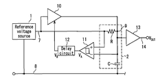
- FIG. 1 is a circuit diagram of a reference voltage generator in a first embodiment of the present invention.
- FIG. 2 is a circuit diagram of a reference voltage generator in a second embodiment of the present invention.
- FIG. 3 is a circuit diagram of a reference voltage generator in a third embodiment of the present invention.
- FIG. 4 is a circuit diagram of a reference voltage generator in a fourth embodiment of the present invention.
- FIG. 5 is a circuit diagram of a reference voltage generator in a fifth embodiment of the present invention.
- FIG. 6 is a circuit diagram showing a configuration example of a voltage buffer circuit in each of the embodiments of the present invention.
- FIG. 7 is a circuit diagram of a reference voltage generator in a first conventional example.
- FIG. 8 is a circuit diagram of a reference voltage generator in a second conventional example.
- FIG. 9 is a graph showing voltage waveforms of the reference voltage generators in the embodiments of the present invention and in the conventional examples by comparison.
- the present invention can be embodied as follows.
- an output impedance of the first voltage buffer circuit is controlled based on a signal obtained by delaying an output signal of the hysteresis comparator by a constant time period. Further, preferably, an output of the low-pass filter is outputted via a second voltage buffer.
- the first switching element is controlled to be off and the second and third switching elements are controlled to be on.
- FIG. 1 is a circuit diagram showing a configuration of a reference voltage generator according to a first embodiment of the present invention.
- a low-pass filter 2 is connected to an output node 7 of a reference voltage source 1 that generates a direct-current voltage that is used as a reference.
- the low-pass filter 2 is a RC primary filter that in the simplest form is a low-pass filter composed of a resistor R and a capacitor C connected in series between the output node 7 and a ground terminal 8 of the reference voltage source 1 .
- a connection point between the resistor R and the capacitor C is an output node 9 of the low-pass filter 2 , at which a voltage obtained by smoothing an output voltage of the reference voltage source 1 is generated. This configuration reduces noise generated by the reference voltage source 1 and the influence of an external disturbance upon the reference voltage source 1 .
- An input terminal of a first voltage buffer circuit 10 further is connected to the output node 7 of the reference voltage source 1 .
- An output terminal of the first voltage buffer circuit 10 is connected to the output node 9 of the low-pass filter 2 .
- the first voltage buffer circuit 10 is switched between two states of its output impedance that are a high output impedance state and a low output impedance state. In the low output impedance state, a ratio between an output voltage and an input voltage, namely, a voltage gain is one time.
- An output V A of a hysteresis comparator 11 is inputted to a control terminal of the first voltage buffer circuit 10 .
- a voltage of the output node 7 that is an output of the reference voltage source 1 is inputted to one input terminal of the hysteresis comparator 11
- a voltage Vout of the output node 9 that is an output of the low-pass filter 2 is inputted to the other input terminal of the hysteresis comparator 11 .
- the reference voltage source 1 When in a steady state, the reference voltage source 1 generates a constant voltage, and as a typical example, a reference voltage source utilizing a band-gap voltage of a semiconductor element can be used.
- low-pass filters may be selected from various types depending on their uses, and a configuration of a low-pass filter is not limited to that in this embodiment. As for a function thereof, it is sufficient that an AC component of a voltage is smoothed between an input of the low-pass filter 2 and the output node 9 to be outputted.
- a high output impedance circuit such as an error amplifier, a voltage buffer, a voltage comparator or the like further are connected to the output node 9 , these have no relation to the basic aspects of the present invention and thus are not shown in the drawings.
- the description is directed next to an operation of the reference voltage generator having the above-described configuration.
- the first voltage buffer circuit 10 When the first voltage buffer circuit 10 is in the high output impedance state, a voltage of the output node 7 of the reference voltage source 1 is smoothed and outputted to the output node 9 of the low-pass filter 2 .
- the first voltage buffer circuit 10 when the first voltage buffer circuit 10 is in the low output impedance state, a voltage of the output node 7 of the reference voltage source 1 is supplied to the output node 9 via the first voltage buffer circuit 10 .
- An output impedance of the first voltage buffer circuit 10 is set to be sufficiently small with respect to an input impedance of the low-pass filter 2 when seen from the output node 9 , and thus the capacitor C of the low-pass filter 2 is charged rapidly at this time. This allows a voltage of the output node 9 of the low-pass filter 2 to approximate rapidly to the voltage of the output node 7 of the reference voltage source 1 .
- the output impedance of the first voltage buffer circuit 10 is controlled by the output V A of the hysteresis comparator 11 in the following manner.
- An operation at power-on of the reference voltage source 1 is as follows. First, in a state where the power of the reference voltage source 1 is cut off or a bias current is cut off externally, a voltage of the output node 7 of the reference voltage source 1 has a value as an initial voltage between a steady state voltage and a potential of the ground terminal 8 , which is normally equal to a potential of the ground terminal 8 . From this state, the cutting off of the power of the reference voltage source 1 is cancelled. This operation is referred to as start-up of the reference voltage source. It can be assumed that the start-up immediately brings the output node 7 to a steady state in the case where the reference voltage source 1 has sufficiently fast response.
- the low-pass filter 2 since the low-pass filter 2 has a time constant determined by parameters and structures of its components, a voltage of the output node 9 cannot be raised immediately. This results in the occurrence of a voltage difference between the output node 9 and the output node 7 .
- the output impedance of the first voltage buffer circuit 10 is controlled so as to be in a low impedance state. This leads to an operation in which the low-pass filter 2 is charged with a low impedance with a target value set to a steady state voltage of the output node 7 . Consequently, as shown by an output waveform E in FIG. 9 , the voltage of the output node 9 rises rapidly.
- the output impedance of the first voltage buffer circuit 10 is controlled so as to be in a high impedance state. This causes a charging current from an output of the first voltage buffer circuit 10 to the low-pass filter 2 to be cut off. From this point in time, the voltage of output node 9 of the low-pass filter 2 gradually approximates to a steady state voltage value of the output node 7 of the reference voltage source 1 with the time constant of the low-pass filter 2 .
- the time constant of the low-pass filter 2 shown in FIG. 1 which is constituted of a RC primary filter, is a product of a resistance value of the resistor R and the capacitance C.
- the voltage difference between the output node 9 and the output node 7 is smaller than the second set value of the hysteresis comparator 11 . Therefore, throughout these time periods, the output V A of the hysteresis comparator 11 has such a value as to maintain the output impedance of the first voltage buffer circuit 10 in the high impedance state.
- the low-pass filter 2 smoothes the voltage of the output node 7 of the reference voltage source 1 so that noise generated by the reference voltage source 1 and an influence of disturbance upon the reference voltage source 1 are reduced, and outputs it to the output node 9 .
- the following can be achieved by setting the second set value of the hysteresis comparator 11 to be sufficiently small. That is, despite the problems of an offset voltage and a delay in response of the hysteresis comparator 11 or a delay in response of the first voltage buffer circuit 10 , unlike the conventional examples, excessive voltage application to a power source voltage side can be suppressed sufficiently, thereby allowing a steady state to be reached rapidly.
- the first set value and the second set value of the hysteresis comparator 11 are set so that the former is sufficiently larger than the latter.
- the first set value and the second set value of the hysteresis comparator 11 can be set to be equal to each other, and thus a comparator without a hysteresis characteristic may be used in place of the hysteresis comparator 11 .
- FIG. 2 is a configuration diagram of a reference voltage generator according to a second embodiment of the present invention.
- This reference voltage generator has a revised configuration of the reference voltage generator according to the first embodiment shown in FIG. 1 , in which the output V A of the hysteresis comparator 11 is inputted to the first voltage buffer circuit 10 via a delay circuit 12 .
- a first voltage buffer circuit 10 is controlled.
- a time required from the time when the output impedance of the first voltage buffer circuit 10 is switched to the high impedance state until the time when the voltage of the output node 9 reaches the steady state is determined by the time constant of the low-pass filter 2 .
- the smaller the second set value of the hysteresis comparator 11 the more the time required for the steady state to be reached is reduced.
- the second set value is set to be smaller than an offset voltage value of the hysteresis comparator 11
- the hysteresis comparator 11 is not switched even when the voltage of the output node 9 reaches a steady state value, and maintains the output impedance of the first voltage buffer circuit 10 in the low impedance state. This causes a voltage of the reference voltage source 1 to be outputted to the output node 9 in a state combined with noise and disturbance to the first voltage buffer circuit 10 .
- an input of the control signal V B to the first voltage buffer circuit 10 is delayed by a predetermined time period from an output V A of a hysteresis comparator 11 .
- a voltage value of an output node 9 reaches a second set value set to be a value not less than an offset voltage value of the hysteresis comparator 11 , an output impedance of the first voltage buffer circuit 10 is maintained in a low impedance state until a lapse of the predetermined time period set by the delay circuit 12 .
- This delay time could be set to a time in the vicinity of or longer than a predicted time required for a steady state to be reached, which is shorter than a time required for a steady state to be reached in the case where the delay circuit 12 is not inserted.
- the delay time can be set to a time relatively shorter than the time required until the steady state is reached in the case where the delay circuit 12 is not inserted.
- a configuration also may be adopted in which instead of using the delay circuit 12 , for example, a capacitor is incorporated into the hysteresis comparator 11 so that the hysteresis comparator 11 itself has a delaying function.
- FIG. 3 is a configuration diagram of a reference voltage generator according to a third embodiment. This embodiment has a revised configuration of the reference voltage generator shown in FIG. 2 , in which the output node 9 of a low-pass filter 2 is connected to an input terminal of a second voltage buffer circuit 13 , and an output terminal 14 of the second voltage buffer circuit 13 is an output terminal of the reference voltage generator.
- This configuration allows an output to be outputted to the output terminal 14 at a low output impedance.
- Most of loads are resistive or capacitive types and thus, in some cases, cannot be driven sufficiently with an output impedance of a low-pass filter 2 . In such cases, impedance conversion is performed by the second voltage buffer circuit 13 , thereby allowing the above-described problem to be solved.
- FIG. 4 is a configuration diagram of a reference voltage generator according to a fourth embodiment. This embodiment is characterized by a revised configuration of the reference voltage generator according to the third embodiment shown in FIG. 3 , in which the second voltage buffer circuit 13 is configured also to have a function as a first voltage buffer circuit 10 (a voltage buffer circuit 15 in this embodiment).
- first to third switching elements 16 to 18 for switching connection are provided.
- high-speed charging and interruption of a low-pass filter 2 are performed by conduction and interruption states of the first to third switching elements 16 to 18 , respectively.
- the conduction and interruption states of first to third switching elements 16 to 18 are controlled based on an output signal of a delay circuit 12 .
- the low-pass filter 2 is connected to an output node 7 of a reference voltage source 1 .
- a voltage obtained by smoothing a voltage of the output node 7 of the reference voltage source 1 is generated, thereby reducing noise generated by the reference voltage source 1 and an influence of disturbance upon the reference voltage source 1 .
- the output node 9 of the low-pass filter 2 is connected to an input terminal of the voltage buffer circuit 15 having a voltage gain of one time via the first switching element 16 .
- the output node 9 further is connected to an output terminal 19 of the voltage buffer circuit 15 via the second switching element 17 .
- a connection point between the first switching element 16 and the voltage buffer circuit 15 is connected to the output node 7 of the reference voltage source 1 via the third switching element 18 .
- the following specifically explains an operation of the reference voltage generator shown in FIG. 4 .
- the first to third switching elements 16 to 18 are controlled through the delay circuit 12 in the following manner.
- this voltage difference is larger than a first set value of the hysteresis comparator 11 , as in the state shown in FIG. 4 , the first switching element 16 is interrupted, while the second switching element 17 and the third switching element 18 are conductive. Thereby a voltage obtained by adding an offset voltage of the voltage buffer circuit 15 to the voltage of the output node 7 is outputted to the output terminal 19 of the voltage buffer circuit 15 with a low impedance.
- the low-pass filter 2 is charged with a low impedance to a steady state voltage of the output node 7 as a target value, and thus the voltage of the output node 9 rises rapidly.
- a noise removing capacitor 20 may be connected between the input terminal of the voltage buffer circuit 15 and a ground terminal 8 . Normally, it is sufficient for the noise removing capacitor 20 to have a small electrostatic capacitance, and a floating capacitance or an input capacitance of the input terminal of the voltage buffer circuit 15 may be used in place thereof. Further, in order to alleviate switching noise, when switching between the conduction and the interruption of the first to third switching elements 16 to 18 , a short time period could be set in which all of the three switching elements are interrupted once.
- FIG. 5 is a configuration diagram of a reference voltage generator according to a fifth embodiment.
- This embodiment has a configuration such that in the reference voltage generator according to the first embodiment shown in FIG. 1 , the state of the output impedance of the first voltage buffer circuit 10 is switched based on a signal from an external terminal 21 instead of a signal of the hysteresis comparator 11 .
- an output impedance of a first voltage buffer circuit 10 is switched to a low impedance, and after a time period controlled by a signal supplied through the external terminal 21 , the output impedance of the first voltage buffer circuit 10 is switched to a high impedance.
- the time period controlled based on the signal supplied through the external terminal 21 is set to a time in the vicinity of or longer than a predicted time required for a steady state to be reached.
- the first voltage buffer circuit 10 in the above-described embodiment can be configured, for example, in the same manner as in a circuit shown in FIG. 6 .
- one of differential input stages composed of transistors 22 and 23 is outputted to an output terminal with a source grounded, and the output terminal is connected directly to a differential negative input terminal so as to feedback negatively, thus constituting an amplifier circuit having a voltage gain of one time.
- a gate of a source grounded transistor 24 is made conductive with respect to a ground terminal by means of a MOS switch 25 , an output is cut off, i.e. an output impedance is turned to be a high impedance. Further, when the MOS switch 25 is interrupted so that the source grounded transistor operates, the output impedance is turned to be low.
- a current drawing ability is not provided, and therefore, when overshoot of an output voltage is expected to occur, a class AB output stage could be used as an output stage so as to provide the drawing ability.
- the present invention allows a reference voltage generator to start-up in a short time and supply a stabilized reference voltage with low noise, and is useful as a reference voltage generator for battery-driven equipment such as a portable communication terminal and the like including a cellular phone.
Landscapes
- Engineering & Computer Science (AREA)
- Physics & Mathematics (AREA)
- Electromagnetism (AREA)
- General Physics & Mathematics (AREA)
- Radar, Positioning & Navigation (AREA)
- Automation & Control Theory (AREA)
- Nonlinear Science (AREA)
- Dc-Dc Converters (AREA)
- Continuous-Control Power Sources That Use Transistors (AREA)
- Control Of Voltage And Current In General (AREA)
- Control Of Electrical Variables (AREA)
Applications Claiming Priority (2)
| Application Number | Priority Date | Filing Date | Title |
|---|---|---|---|
| JP2008-326442 | 2008-12-22 | ||
| JP2008326442A JP2010146526A (ja) | 2008-12-22 | 2008-12-22 | 基準電圧発生回路 |
Publications (2)
| Publication Number | Publication Date |
|---|---|
| US20100156520A1 US20100156520A1 (en) | 2010-06-24 |
| US8044708B2 true US8044708B2 (en) | 2011-10-25 |
Family
ID=42265113
Family Applications (1)
| Application Number | Title | Priority Date | Filing Date |
|---|---|---|---|
| US12/643,277 Expired - Fee Related US8044708B2 (en) | 2008-12-22 | 2009-12-21 | Reference voltage generator |
Country Status (2)
| Country | Link |
|---|---|
| US (1) | US8044708B2 (ja) |
| JP (1) | JP2010146526A (ja) |
Cited By (7)
| Publication number | Priority date | Publication date | Assignee | Title |
|---|---|---|---|---|
| US20170213518A1 (en) * | 2016-01-27 | 2017-07-27 | Mitsubishi Electric Corporation | Drive device and liquid crystal display apparatus |
| US9829904B2 (en) * | 2015-02-02 | 2017-11-28 | Sii Semiconductor Corporation | Low-pass filter circuit and power supply device |
| CN113809921A (zh) * | 2020-06-17 | 2021-12-17 | 和硕联合科技股份有限公司 | 电源电路和电源装置 |
| US11378991B1 (en) * | 2021-06-23 | 2022-07-05 | Nxp B.V. | Soft-start circuit for voltage regulator |
| US20220229456A1 (en) * | 2021-01-15 | 2022-07-21 | Realtek Semiconductor Corporation | Voltage generation circuit and associated capacitor charging method and system |
| CN114815940A (zh) * | 2021-01-22 | 2022-07-29 | 瑞昱半导体股份有限公司 | 电压产生电路及相关电容充电方法和系统 |
| EP4296816A1 (en) * | 2022-06-20 | 2023-12-27 | Key ASIC Inc. | Bandgap module and linear regulator |
Families Citing this family (17)
| Publication number | Priority date | Publication date | Assignee | Title |
|---|---|---|---|---|
| CN102650892B (zh) * | 2011-02-25 | 2016-01-13 | 瑞昱半导体股份有限公司 | 参考电压稳定装置及相关的电压稳定方法 |
| DE102011089402B4 (de) * | 2011-04-28 | 2015-07-16 | Zentrum Mikroelektronik Dresden Ag | Anordnung und Verfahren zur Erzeugung einer Ausgangsspannung |
| JP6001876B2 (ja) * | 2012-02-24 | 2016-10-05 | ラピスセミコンダクタ株式会社 | 基準電圧中継回路 |
| US9110643B2 (en) | 2012-06-11 | 2015-08-18 | Arm Limited | Leakage current reduction in an integrated circuit |
| US9374545B2 (en) * | 2013-09-13 | 2016-06-21 | BAE Systems Imaging Solutions Inc. | Amplifier adapted for CMOS imaging sensors |
| GB2520290B (en) * | 2013-11-14 | 2018-02-28 | Advanced Risc Mach Ltd | Leakage current reduction in an integrated circuit |
| US10468917B2 (en) * | 2014-03-05 | 2019-11-05 | Ricoh Co., Ltd. | Battery charger |
| US10298071B2 (en) | 2014-03-05 | 2019-05-21 | Ricoh Co., Ltd | DC-DC boost converter |
| CN105373178B (zh) | 2014-08-15 | 2018-02-02 | 深圳市中兴微电子技术有限公司 | 电路启动方法、控制电路及电压基准电路 |
| CN106325351A (zh) * | 2016-10-14 | 2017-01-11 | 广州昌钰行信息科技有限公司 | 一种双路电压缓冲电路 |
| US10401942B2 (en) * | 2017-02-22 | 2019-09-03 | Ambiq Micro Inc. | Reference voltage sub-system allowing fast power up from extended periods of ultra-low power standby mode |
| US11252353B2 (en) * | 2017-06-29 | 2022-02-15 | BAE Systems Imaging Solutions Inc. | Ultra-low noise amplifier adapted for CMOS imaging sensors |
| FR3113213B1 (fr) * | 2020-07-30 | 2023-03-10 | Autovib | Circuit pour fournir une tension de référence filtrée et dispositif d’alimentation exploitant un tel circuit |
| US12451890B2 (en) * | 2023-03-22 | 2025-10-21 | Nanya Technology Corporation | Power down circuit and power down method |
| CN116483154B (zh) * | 2023-06-25 | 2023-09-12 | 上海海栎创科技股份有限公司 | 一种低延迟基准输出电路与输出方法 |
| CN117369580A (zh) * | 2023-11-24 | 2024-01-09 | 思瑞浦微电子科技(上海)有限责任公司 | 电压源输出电路及控制方法 |
| CN119717975A (zh) * | 2024-12-04 | 2025-03-28 | 紫光同芯微电子有限公司 | 低压差线性稳压器电路和片上系统 |
Citations (10)
| Publication number | Priority date | Publication date | Assignee | Title |
|---|---|---|---|---|
| JPH06301429A (ja) | 1993-04-13 | 1994-10-28 | Hitachi Ltd | 基準電圧発生回路 |
| JPH08272461A (ja) | 1995-03-30 | 1996-10-18 | Seiko Instr Inc | ボルテージ・レギュレータ |
| US5859563A (en) * | 1997-02-13 | 1999-01-12 | Texas Instruments Incorporated | Low-noise low-impedance voltage reference |
| US5886565A (en) * | 1996-09-30 | 1999-03-23 | Yamaha Corporation | Reference voltage generating circuit having an integrator |
| US5889392A (en) | 1997-03-06 | 1999-03-30 | Maxim Integrated Products, Inc. | Switch-mode regulators and methods providing transient response speed-up |
| US5892381A (en) | 1997-06-03 | 1999-04-06 | Motorola, Inc. | Fast start-up circuit |
| US5959439A (en) | 1997-05-23 | 1999-09-28 | The Board Of Trustees Of The University Of Illinois | Monolithic DC to DC converter |
| JP2002023870A (ja) | 2000-07-10 | 2002-01-25 | Ricoh Co Ltd | 基準電圧回路および該基準電圧回路を用いたボルテージ・レギュレータ |
| JP2005346522A (ja) | 2004-06-04 | 2005-12-15 | Toko Inc | ノイズパスコンデンサの充電回路 |
| US7362081B1 (en) | 2005-02-02 | 2008-04-22 | National Semiconductor Corporation | Low-dropout regulator |
Family Cites Families (3)
| Publication number | Priority date | Publication date | Assignee | Title |
|---|---|---|---|---|
| JP3643389B2 (ja) * | 1994-07-27 | 2005-04-27 | 株式会社東芝 | 定電圧回路 |
| JP2001306167A (ja) * | 2000-04-25 | 2001-11-02 | Fuji Electric Co Ltd | 基準電圧回路 |
| JP4889398B2 (ja) * | 2006-07-27 | 2012-03-07 | 株式会社リコー | 定電圧電源回路 |
-
2008
- 2008-12-22 JP JP2008326442A patent/JP2010146526A/ja active Pending
-
2009
- 2009-12-21 US US12/643,277 patent/US8044708B2/en not_active Expired - Fee Related
Patent Citations (10)
| Publication number | Priority date | Publication date | Assignee | Title |
|---|---|---|---|---|
| JPH06301429A (ja) | 1993-04-13 | 1994-10-28 | Hitachi Ltd | 基準電圧発生回路 |
| JPH08272461A (ja) | 1995-03-30 | 1996-10-18 | Seiko Instr Inc | ボルテージ・レギュレータ |
| US5886565A (en) * | 1996-09-30 | 1999-03-23 | Yamaha Corporation | Reference voltage generating circuit having an integrator |
| US5859563A (en) * | 1997-02-13 | 1999-01-12 | Texas Instruments Incorporated | Low-noise low-impedance voltage reference |
| US5889392A (en) | 1997-03-06 | 1999-03-30 | Maxim Integrated Products, Inc. | Switch-mode regulators and methods providing transient response speed-up |
| US5959439A (en) | 1997-05-23 | 1999-09-28 | The Board Of Trustees Of The University Of Illinois | Monolithic DC to DC converter |
| US5892381A (en) | 1997-06-03 | 1999-04-06 | Motorola, Inc. | Fast start-up circuit |
| JP2002023870A (ja) | 2000-07-10 | 2002-01-25 | Ricoh Co Ltd | 基準電圧回路および該基準電圧回路を用いたボルテージ・レギュレータ |
| JP2005346522A (ja) | 2004-06-04 | 2005-12-15 | Toko Inc | ノイズパスコンデンサの充電回路 |
| US7362081B1 (en) | 2005-02-02 | 2008-04-22 | National Semiconductor Corporation | Low-dropout regulator |
Cited By (14)
| Publication number | Priority date | Publication date | Assignee | Title |
|---|---|---|---|---|
| US9829904B2 (en) * | 2015-02-02 | 2017-11-28 | Sii Semiconductor Corporation | Low-pass filter circuit and power supply device |
| TWI657658B (zh) * | 2015-02-02 | 2019-04-21 | 日商艾普凌科有限公司 | 低通濾波器電路以及電源裝置 |
| US20170213518A1 (en) * | 2016-01-27 | 2017-07-27 | Mitsubishi Electric Corporation | Drive device and liquid crystal display apparatus |
| US10720119B2 (en) * | 2016-01-27 | 2020-07-21 | Mitsubishi Electric Corporation | Drive device and liquid crystal display apparatus |
| CN113809921A (zh) * | 2020-06-17 | 2021-12-17 | 和硕联合科技股份有限公司 | 电源电路和电源装置 |
| US20210397208A1 (en) * | 2020-06-17 | 2021-12-23 | Pegatron Corporation | Power supply circuit and power supply device |
| CN113809921B (zh) * | 2020-06-17 | 2024-07-26 | 和硕联合科技股份有限公司 | 电源电路和电源装置 |
| US11586234B2 (en) * | 2020-06-17 | 2023-02-21 | Pegatron Corporation | Power supply device |
| US11520366B2 (en) * | 2021-01-15 | 2022-12-06 | Realtek Semiconductor Corporation | Voltage generation circuit and associated capacitor charging method and system |
| US20220229456A1 (en) * | 2021-01-15 | 2022-07-21 | Realtek Semiconductor Corporation | Voltage generation circuit and associated capacitor charging method and system |
| CN114815940A (zh) * | 2021-01-22 | 2022-07-29 | 瑞昱半导体股份有限公司 | 电压产生电路及相关电容充电方法和系统 |
| CN114815940B (zh) * | 2021-01-22 | 2024-01-30 | 瑞昱半导体股份有限公司 | 电压产生电路及相关电容充电方法和系统 |
| US11378991B1 (en) * | 2021-06-23 | 2022-07-05 | Nxp B.V. | Soft-start circuit for voltage regulator |
| EP4296816A1 (en) * | 2022-06-20 | 2023-12-27 | Key ASIC Inc. | Bandgap module and linear regulator |
Also Published As
| Publication number | Publication date |
|---|---|
| US20100156520A1 (en) | 2010-06-24 |
| JP2010146526A (ja) | 2010-07-01 |
Similar Documents
| Publication | Publication Date | Title |
|---|---|---|
| US8044708B2 (en) | Reference voltage generator | |
| TWI437404B (zh) | Voltage regulator | |
| US8018214B2 (en) | Regulator with soft-start using current source | |
| US8508196B2 (en) | Switching regulator | |
| US8242760B2 (en) | Constant-voltage circuit device | |
| US9293990B2 (en) | Switching regulator and electronic apparatus | |
| US7969132B2 (en) | Switching power supply unit and control method of switching power supply unit | |
| US9553514B2 (en) | DC-DC converter | |
| US20030185028A1 (en) | Power supply unit having a soft start functionality and portable apparatus equipped with such power supply unit | |
| US20160301309A1 (en) | On-period setting circuit, power control ic, and switching power supply device | |
| US20130049721A1 (en) | Linear Regulator and Control Circuit Thereof | |
| US9608521B2 (en) | DC/DC converter activation stability control | |
| JP6761361B2 (ja) | 電源装置 | |
| JP4651428B2 (ja) | スイッチングレギュレータ及びこれを備えた電子機器 | |
| US11444538B2 (en) | Switching regulator based on load estimation and operating method thereof | |
| US20110140678A1 (en) | Current limit recovery circuit | |
| US9166468B2 (en) | Voltage regulator circuit with soft-start function | |
| US11909369B2 (en) | Low-pass filter circuit | |
| JP5068631B2 (ja) | 定電圧回路 | |
| CN113484590A (zh) | 一种开关电源小电流检测电路及开关电源小电流控制方法 | |
| US11994892B2 (en) | Shunt regulator | |
| JP6850199B2 (ja) | 電源回路 | |
| US9952616B2 (en) | Differential circuit including a current mirror | |
| JP2017126285A (ja) | ボルテージレギュレータ | |
| US12388435B2 (en) | Power limiting circuits |
Legal Events
| Date | Code | Title | Description |
|---|---|---|---|
| AS | Assignment |
Owner name: PANASONIC CORPORATION,JAPAN Free format text: ASSIGNMENT OF ASSIGNORS INTEREST;ASSIGNOR:KUME, TOMOHIRO;REEL/FRAME:024226/0048 Effective date: 20091208 Owner name: PANASONIC CORPORATION, JAPAN Free format text: ASSIGNMENT OF ASSIGNORS INTEREST;ASSIGNOR:KUME, TOMOHIRO;REEL/FRAME:024226/0048 Effective date: 20091208 |
|
| STCF | Information on status: patent grant |
Free format text: PATENTED CASE |
|
| FEPP | Fee payment procedure |
Free format text: PAYOR NUMBER ASSIGNED (ORIGINAL EVENT CODE: ASPN); ENTITY STATUS OF PATENT OWNER: LARGE ENTITY |
|
| FPAY | Fee payment |
Year of fee payment: 4 |
|
| FEPP | Fee payment procedure |
Free format text: MAINTENANCE FEE REMINDER MAILED (ORIGINAL EVENT CODE: REM.); ENTITY STATUS OF PATENT OWNER: LARGE ENTITY |
|
| LAPS | Lapse for failure to pay maintenance fees |
Free format text: PATENT EXPIRED FOR FAILURE TO PAY MAINTENANCE FEES (ORIGINAL EVENT CODE: EXP.); ENTITY STATUS OF PATENT OWNER: LARGE ENTITY |
|
| STCH | Information on status: patent discontinuation |
Free format text: PATENT EXPIRED DUE TO NONPAYMENT OF MAINTENANCE FEES UNDER 37 CFR 1.362 |
|
| FP | Lapsed due to failure to pay maintenance fee |
Effective date: 20191025 |