US8050558B2 - Optical signal sampling apparatus and method and optical signal monitor apparatus and method using the same - Google Patents
Optical signal sampling apparatus and method and optical signal monitor apparatus and method using the same Download PDFInfo
- Publication number
- US8050558B2 US8050558B2 US12/308,264 US30826408A US8050558B2 US 8050558 B2 US8050558 B2 US 8050558B2 US 30826408 A US30826408 A US 30826408A US 8050558 B2 US8050558 B2 US 8050558B2
- Authority
- US
- United States
- Prior art keywords
- optical
- sampling
- signal
- optical signal
- light pulse
- Prior art date
- Legal status (The legal status is an assumption and is not a legal conclusion. Google has not performed a legal analysis and makes no representation as to the accuracy of the status listed.)
- Expired - Fee Related, expires
Links
Images


Classifications
-
- G—PHYSICS
- G01—MEASURING; TESTING
- G01J—MEASUREMENT OF INTENSITY, VELOCITY, SPECTRAL CONTENT, POLARISATION, PHASE OR PULSE CHARACTERISTICS OF INFRARED, VISIBLE OR ULTRAVIOLET LIGHT; COLORIMETRY; RADIATION PYROMETRY
- G01J11/00—Measuring the characteristics of individual optical pulses or of optical pulse trains
Definitions
- the present invention relates to an optical signal sampling apparatus and method and an optical signal monitor apparatus and method using the optical signal sampling apparatus and method, or in particular, an optical signal sampling apparatus and method employing a technique capable of sampling, with a sufficient resolution and a high accuracy, the waveform information of the optical signal modulated by a fast data signal, and an optical signal monitor apparatus and method capable of accurately monitoring the optical signal using the particular optical signal sampling apparatus and method.
- the quality of the optical signal propagated on the network is required to be monitored by an optical signal monitor apparatus.
- the optical signal monitor apparatus acquires the waveform information of the signal on a transmission path and by calculating a value indicating the signal quality from the waveform information, outputs the calculation result thereof. It is very difficult to acquire the waveform information by receiving, directly with a light receiver, the optical signal modulated by the data signal of a very high bit rate of several tens of Gb/s.
- the conventional optical signal monitor apparatus uses the equivalent time sampling scheme to acquire the waveform information of the fast optical signal.
- the waveform P′ plotted by the envelope connecting the instantaneous amplitude values thus acquired is a waveform of the optical signal P enlarged by Ts/ ⁇ T times on the time axis, and holds the features of the waveform of the original optical signal P.
- the probability distribution of the amplitude indicating one of the binary levels and the amplitude of another is determined, and by calculating the standard deviation thereof, the Q value indicating the signal quality can be obtained.
- Patent Document 1 The aforementioned technique of the equivalent time sampling of the optical signal and calculating the Q value indicating the signal quality from the waveform information thus obtained is disclosed in Patent Document 1.
- a bulk-type nonlinear optical member is used normally as an element for the equivalent time sampling of the optical signal.
- This nonlinear optical member is generally low in sampling efficiency (the sampling efficiency using the wavelength conversion phenomenon, i.e. the wavelength conversion efficiency is ⁇ 20 dB or less).
- sampling efficiency using the wavelength conversion phenomenon i.e. the wavelength conversion efficiency is ⁇ 20 dB or less.
- a high S/N can be obtained for the waveform information of a strong optical signal, therefore, the problem is that a sufficient S/N cannot be obtained for the waveform information of a weak optical signal.
- the use is conceived of an electroabsorption modulator remarkably lower in transmission loss than the nonlinear optical member, i.e. substantially high in sampling efficiency as an element for the equivalent time sampling of the optical signal.
- the electroabsorption modulator has such a characteristic that the absorption rate of the light passed through the optical path connecting two optical terminals is changed in accordance with the magnitude of the electric field applied in the light path. Only during the time when the optical signal is applied to one of the optical terminals and the electricity sampling pulse signal applied to a power supply terminal to input the sampling pulse signal, the absorption rate of the optical signal is reduced so that the optical signal is emitted from another optical terminal thereby to sample the optical signal.
- An object of this invention is to solve the problems of the prior art described above and to provide an optical signal sampling apparatus and method having a high sampling efficiency and capable of sampling the waveform information of a fast optical signal accurately with a sufficiently high resolution, and an optical signal monitor apparatus and method capable of obtaining an eye pattern of the optical signal in stable fashion and accurately monitoring the optical signal using the optical signal sampling apparatus and method.
- an optical signal sampling apparatus comprising:
- a sampling light pulse generating unit which generates a sampling light pulse (Ps) having a predetermined period to sample an optical signal to be sampled (Px);
- an optical sampling unit ( 22 ) which samples the optical signal to be sampled (Px), with the sampling light pulse (Ps) from the sampling light pulse generating unit ( 21 ) and emits an optical pulse signal (Pz) obtained by the sampling,
- optical sampling unit ( 22 ) includes:
- an optical combiner ( 23 ) which combines the optical signal to be sampled (Px) and the sampling light pulse (Ps) from the sampling light pulse generating unit ( 21 ) with each other;
- an electroabsorption modulator ( 24 ) having two optical terminals ( 24 a , 24 b ) for inputting/outputting light and a power supply terminal ( 24 c ) for applying an electric field to an optical path connecting the two optical terminals ( 24 a , 24 b ), the electroabsorption modulator ( 24 ) having such a characteristic that an absorption rate of the light propagating through the optical path is changed in accordance with the magnitude of the electric field, one terminal ( 24 a ) of the two optical terminals ( 24 a , 24 b ) receiving the light (Py) emitted from the optical combiner ( 23 );
- a DC power supply which applies, to the power supply terminal ( 24 c ) of the electroabsorption modulator ( 24 ), a predetermined DC voltage (Vdc) for sampling the optical signal to be sampled (Px), with the sampling light pulse (Ps) in the electroabsorption modulator ( 24 ) by increasing the absorption rate in the absence of the sampling light pulse (Ps) incident to the electroabsorption modulator ( 24 ) and decreasing the absorption rate in the presence of the sampling light pulse (Ps) incident to the electroabsorption modulator ( 24 ), thereby emitting an optical signal (Py′) obtained by the sampling from another terminal ( 24 b ) of the two optical terminals ( 24 a , 24 b ); and
- an optical separator ( 26 , 26 ′) which selectively emits an optical signal component (Pz) to be sampled, of the optical signal (Py′) emitted from the other terminal ( 24 b ) of the two optical terminals ( 24 a , 24 b ) of the electroabsorption modulator ( 24 ).
- a wavelength of the sampling light pulse (Ps) is different from a wavelength of the optical signal to be sampled (Px), and
- the optical separator ( 26 , 26 ′) is configured of a wavelength filter ( 26 ) for selectively emitting the optical pulse signal (Pz) having a wavelength component of the optical signal to be sampled (Px), of the optical signal (Py′) emitted from the other terminal ( 24 b ) of the two optical terminals ( 24 a , 24 b ) of the electroabsorption modulator ( 24 ).
- the optical combiner ( 23 ) is configured to combine the optical signal to be sampled (Px) and the sampling light pulse (Ps) with each other by means of polarized waves orthogonal to each other, and
- the optical separator ( 26 , 26 ′) is configured of a polarization filter ( 26 ′) for selectively emitting the optical signal (Pz) having a polarization component of the optical signal to be sampled (Px), of the optical signal (Py′) emitted from the other terminal ( 24 b ) of the two optical terminals ( 24 a , 24 b ) of the electroabsorption modulator ( 24 ).
- the sampling light pulse generating unit ( 21 ) includes:
- a reference signal generator configured as a synthesizer which generates a stable signal (Ra) having a period Ts corresponding to the period of the sampling light pulse (Ps);
- a multiplier ( 21 b ) which multiplies the stable signal (Ra) having the period Ts generated by the reference signal generator ( 21 a ), by M (M: integer larger than 1), and output as a signal (Rb) multiplied by M;
- a light source ( 21 d ) which emits continuous light (Pcw);
- an optical modulator ( 21 c ) which emits an optical pulse (Pa) having a period Ts/M by modulating the continuous light (Pcw) emitted from the light source ( 21 d ) with the signal (Rb) multiplied by M output from the multiplier ( 21 b );
- an optical gate circuit ( 21 e ) which converts the optical pulse (Pa) emitted from the optical modulator ( 21 c ) into an optical pulse (Pb) having a period Ts by thinning the optical pulse (Pa) to 1/M;
- a dispersion decreasing fiber ( 21 f ) which further narrows the pulse width of the optical pulse (Pb) having the period Ts converted by the optical gate circuit ( 21 e ) and emits as the sampling light pulse (Ps).
- a parameter setting unit ( 28 ) which receives the information on a clock period Tc of a data signal modulating the optical signal to be sampled (Px) or a bit rate and a predetermined offset time ⁇ T of the data signal, and determines the sampling period Ts of the sampling light pulse (Ps) by an arithmetic operation of
- the optical signal sampling apparatus according to the first aspect, wherein the sampling light pulse generating unit ( 21 ) is configured of a short pulse generating unit ( 21 g ) having a function of generating by self-excited oscillation a short pulse having a frequency different by one integer-th from the frequency of the optical signal to be sampled (Px) and shifting the short-pulse frequency.
- the sampling light pulse generating unit ( 21 ) is configured of a short pulse generating unit ( 21 g ) having a function of generating by self-excited oscillation a short pulse having a frequency different by one integer-th from the frequency of the optical signal to be sampled (Px) and shifting the short-pulse frequency.
- an optical signal monitor apparatus comprising:
- an optical signal sampling apparatus having a sampling light pulse generating unit ( 21 ) which emits a sampling light pulse (Ps) having a period different by a predetermined offset time from an integer multiple of a clock period (Tc) of a data signal modulating an optical signal to be monitored (Px); and an optical sampling unit ( 22 ) which samples the optical signal to be monitored (Px), by the sampling light pulse (Ps) from the sampling light pulse generating unit ( 21 ) and emits an optical pulse signal (Pz) obtained by the sampling; and
- a photoelectric converter ( 30 ) which receives the optical pulse signal (Pz) emitted from the optical sampling unit ( 22 ) of the optical signal sampling apparatus ( 100 ) and converts the optical pulse signal into an electric signal (Ez) thereby to acquire waveform information of the optical signal to be monitored (Px),
- an electroabsorption modulator ( 24 ) having two optical terminals ( 24 a , 24 b ) for inputting/outputting light and a power supply terminal ( 24 c ) for applying an electric field to an optical path connecting the two optical terminals ( 24 a , 24 b ), the electroabsorption modulator ( 24 ) having such a characteristic that an absorption rate of the light propagating through the optical path changes in accordance with the magnitude of the electric field, one terminal ( 24 a ) of the two optical terminals ( 24 a , 24 b ) receiving the light (Py) emitted from the optical combiner ( 23 );
- a DC power supply which increases the absorption rate in the absence of the sampling light pulse (Ps) incident to the electroabsorption modulator ( 24 ) and decreases the absorption rate in the presence of the sampling light pulse (Ps) incident to the electroabsorption modulator ( 24 ) so that the electroabsorption modulator ( 24 ) samples the optical signal to be sampled (Px), with the sampling light pulse (Ps) and applies a predetermined DC voltage (Vdc) to the power supply terminal ( 24 c ) of the electroabsorption modulator ( 24 ) to emit an optical signal (Py′) obtained by the sampling from another terminal ( 24 b ) of the two optical terminals ( 24 a , 24 b ); and
- the optical signal monitor apparatus according to the seventh aspect, wherein a wavelength of the sampling light pulse (Ps) is different from a wavelength of the optical signal to be monitored (Px), and
- the optical separator ( 26 , 26 ′) of the optical signal sampling apparatus ( 100 ) is configured of a wavelength filter ( 26 ) for selectively emitting the optical signal (Pz) having a wavelength component of the optical signal to be monitored (Px), of the optical signals (Py′) emitted from the other terminal ( 24 b ) of the two optical terminals ( 24 a , 24 b ) of the electroabsorption modulator ( 24 ).
- the optical signal monitor apparatus according to the seventh aspect, wherein the optical combiner ( 23 ) of the optical signal sampling apparatus ( 100 ) is configured to combine the optical signal to be monitored (Px) and the sampling light pulse (Ps) with each other using polarized waves orthogonal to each other, and the optical separator ( 26 , 26 ′) of the optical signal sampling apparatus ( 100 ) is configured of a polarization filter ( 26 ′) for selectively emitting the optical signal (Pz) having a polarization component of the optical signal to be monitored (Px), of the optical signals (Py′) emitted from the other terminal ( 24 b ) of the two optical terminals ( 24 a , 24 b ) of the electroabsorption modulator ( 24 ).
- the optical combiner ( 23 ) of the optical signal sampling apparatus ( 100 ) is configured to combine the optical signal to be monitored (Px) and the sampling light pulse (Ps) with each other using polarized waves orthogonal to each other
- the sampling light pulse generating unit ( 21 ) of the optical signal sampling apparatus ( 100 ) includes:
- a reference signal generator configured as a synthesizer which generates a stable signal (Ra) having a period Ts corresponding to a period of the sampling light pulse (Ps);
- a multiplier ( 21 b ) which multiplies the stable signal (Ra) having the period Ts generated by the reference signal generator ( 21 a ) by M (M: integer larger than 1), output as a signal (Rb) multiplied by M;
- a light source ( 21 d ) which emits continuous light (Pcw);
- an optical modulator ( 21 c ) which emits an optical pulse (Pa) having a period Ts/M by modulating the continuous light (Pcw) emitted from the light source ( 21 d ) with the signal (Rb) multiplied by M output from the multiplier ( 21 b );
- an optical gate circuit ( 21 e ) which converts the optical pulse (Pa) emitted from the optical modulator ( 21 c ) into an optical pulse (Pb) having the period Ts by thinning the optical pulse (Pa) to 1/M;
- a dispersion decreasing fiber ( 21 f ) which further narrows the pulse width of the optical pulse (Pb) having the period Ts converted by the optical gate circuit ( 21 e ) and emits as the sampling light pulse (Ps).
- a parameter setting unit ( 28 ) which receives the information on a clock period Tc of a data signal modulating the optical signal to be monitored (Px) or a bit rate and a predetermined offset time ⁇ T of the data signal, and determines the sampling period Ts of the sampling light
- a fundamental wave component signal output unit ( 41 ) which outputs a fundamental wave component signal (U) of a frequency equal to a fundamental wave component of an envelope wave of an output signal (Ez) from the photoelectric converter ( 30 );
- a comparator ( 42 ) which compares the fundamental wave component signal (U) from the fundamental wave component signal output unit ( 41 ) with a predetermined threshold value (Vr);
- a data acquisition control unit ( 44 ) which starts the acquisition of the waveform information on the output signal (Ez) from the photoelectric converter ( 30 ) from the timing when the fundamental wave component signal (U) exceeds the predetermined threshold value (Vr) in a comparing operation of the comparator ( 42 ).
- the optical signal monitor apparatus according to the fourteenth aspect, wherein the sampling clock (Es) is output in synchronism with the sampling light pulse (Ps) by the sampling light pulse generating unit ( 21 ).
- the fundamental wave component signal output unit ( 41 ), configured as a PLL (phase locked loop), includes:
- a voltage-controlled oscillator ( 41 b ) which outputs an oscillation output signal having a predetermined oscillation frequency
- phase comparator ( 41 c ) which outputs a control signal (Vc) corresponding to a phase difference between an output signal of the narrow-band of bandpass filter ( 41 a ) and the output signal of the voltage-controlled oscillator ( 41 b ),
- the oscillation frequency of the voltage-controlled oscillator ( 41 b ) is controlled by the control signal (Vc) output from the phase comparator ( 41 c ) and a phase of the oscillation output signal is synchronized with a phase of the output signal of narrow-band of the bandpass filter ( 41 a ) thereby to output a synchronized sinusoidal oscillation output signal as the fundamental wave component signal (U).
- the optical signal monitor apparatus wherein the data acquisition control unit ( 44 ) repeats, a predetermined number of times (H), an operation in which the data signal (Dz) begins to be written in the waveform memory ( 45 ) from the timing when the fundamental wave component signal (U) exceeds the threshold value (Vr) in the comparator ( 42 ), and after completely writing a predetermined number (W) of the data signal, the operation stands by until the timing when the fundamental wave component signal (U) exceeds the threshold value (Vr) again, the predetermined number (W) of the data signal (Dz) being written in the plurality (H) of the different areas of the waveform memory ( 45 ) in order of address, respectively.
- the data acquisition control unit ( 44 ) repeats, a predetermined number of times (H), an operation in which the data signal (Dz) begins to be written in the waveform memory ( 45 ) from the timing when the fundamental wave component signal (U) exceeds the threshold value (Vr) in the comparator ( 42 ), and after completely writing a pre
- the optical signal monitor apparatus further comprising an arithmetic operation unit ( 35 ′) which calculates a value indicating the quality of the optical signal to be monitored (Px), based on the data signal (Dz) written in the waveform memory ( 45 ).
- the optical signal monitor apparatus according to the nineteenth aspect, wherein the arithmetic operation unit ( 35 ′) compares the data signal (Dz) written in the waveform memory ( 45 ) with a predetermined threshold value, and by separating the data signals into a sample value associated with the data “1” and a sample value associated with the data “0”, determines average values and standard deviation of sample value groups for each of the data thereby to determine a ratio ⁇ / ⁇ between a difference ⁇ of the average values and a sum ⁇ of the standard deviations as a quality value Q.
- the optical signal monitor apparatus according to the nineteenth aspect, wherein the arithmetic operation unit ( 35 ′) capable of obtaining an eye pattern by superposing, in the order of address, the predetermined number (W) of the data signals (Dz) as the waveform data (Dz) of a predetermined number of bits stored in each session in the order of address in the plurality (H) of different areas of the waveform memory ( 45 ).
- the arithmetic operation unit ( 35 ′) capable of obtaining an eye pattern by superposing, in the order of address, the predetermined number (W) of the data signals (Dz) as the waveform data (Dz) of a predetermined number of bits stored in each session in the order of address in the plurality (H) of different areas of the waveform memory ( 45 ).
- an optical signal sampling method comprising:
- a sampling light pulse generating step for generating a sampling light pulse (Ps) of a predetermined period to sample an optical signal to be sampled (Px);
- an optical sampling step for sampling the optical signal to be sampled (Px), with the sampling light pulse (Ps) from the sampling light pulse generating unit ( 21 ) and emitting an optical pulse signal (Pz) obtained by the sampling,
- optical sampling step includes:
- an electroabsorption modulator ( 24 ) having two optical terminals ( 24 a , 24 b ) for inputting/outputting light and a power supply terminal ( 24 c ) for applying an electric field to an optical path connecting the two optical terminals ( 24 a , 24 b ), the modulator having such a characteristic that an absorption rate of the light propagating through the optical path is changed in accordance with the magnitude of the electric field, one terminal ( 24 a ) of the two optical terminals ( 24 a , 24 b ) receiving the light (Py) emitted from the optical combiner ( 23 );
- an optical signal monitor method comprising:
- a sampling light pulse generating step for emitting a sampling light pulse (Ps) having a period different by a predetermined offset time from an integer multiple of a clock period (Tc) of the data signal modulating the optical signal to be monitored (Px);
- an optical sampling step for sampling the optical signal to be monitored (Px), by a sampling light pulse (Ps) and emitting an optical pulse signal (Pz) obtained by the sampling;
- a photoelectric conversion step for acquiring the waveform information of the optical signal to be monitored (Px), by receiving the optical pulse signal (Pz) emitted from the optical sampling unit ( 22 ) of the optical signal sampling apparatus ( 100 ) and converting the optical pulse signal (Pz) into an electric signal (Ez),
- an electroabsorption modulator ( 24 ) having two optical terminals ( 24 a , 24 b ) for inputting and outputting light and a power supply terminal ( 24 c ) for applying an electric field to an optical path connecting the two optical terminals ( 24 a , 24 b ), the electroabsorption modulator ( 24 ) having such a characteristic that an absorption rate of the light propagating through the optical path changes in accordance with the magnitude of the electric field, one terminal ( 24 a ) of the two optical terminals ( 24 a , 24 b ) receiving the light (Py) emitted from the optical combiner ( 23 );
- an electroabsorption modulator is used as a sampling element, and an optical signal to be sampled and a sampling light pulse are combined and applied to one of the optical terminals of the modulator, while the power supply terminal is supplied with a predetermined DC voltage indicating a high absorption rate in the absence of an incident sampling light pulse and a low absorption rate in the presence of an incident sampling light pulse, while the component of the optical signal is selectively emitted from the light emitted from the other optical terminal in the presence of an incident sampling light pulse.
- a light pulse having a narrow width can be used for sampling, and the loss of the optical signal can be reduced.
- the sampling efficiency is improved substantially, and the waveform information for even a weak optical signal can be obtained accurately.
- the fundamental wave component signal is extracted from the signal obtained by sampling the optical signal, and the waveform information begins to be acquired from the timing when the fundamental wave component signal exceeds a threshold value. Therefore, the waveform information acquisition start timing can be synchronized with the data signal modulated on the actually incident optical signal, and by superposing plural sets of waveform information obtained at the start timing, an eye pattern can be obtained in stable fashion.
- FIG. 2 is a block diagram shown for explaining an example of the configuration of the essential parts of FIG. 1 .
- FIG. 3 is a diagram shown for explaining an example of the characteristics of the essential parts of FIG. 1 .
- FIG. 4 is a waveform diagram shown for explaining the operation against the optical signal having a repetitive waveform as the operation of the first embodiment configured as shown in FIG. 1 .
- FIG. 5 is a waveform diagram shown for explaining the operation against the optical signal having no repetitive waveform as the operation of the first embodiment configured as shown in FIG. 1 .
- FIG. 6 is a block diagram shown for explaining the configuration of the optical signal sampling apparatus and method and the optical signal monitor apparatus and method using the same according to a second embodiment of the invention.
- FIG. 7 is a block diagram shown for explaining an example of the configuration of the essential parts of FIG. 6 .
- FIG. 8 is a waveform diagram shown for explaining the operation against the optical signal having a repetitive waveform as the operation of the second embodiment configured as shown in FIG. 6 .
- FIG. 9 is a waveform diagram shown for explaining an example of storage of the waveform obtained by sampling as the operation according to the second embodiment configured as shown in FIG. 6 .
- FIG. 10 is a waveform diagram shown for explaining the eye pattern obtained by superpositioning of the waveforms stored in FIG. 9 .
- FIG. 11 is a waveform diagram shown for explaining the operation against the optical signal having no repetitive waveform as the operation of the second embodiment configured as shown in FIG. 6 .
- FIG. 12 is a block diagram shown for explaining the configuration of the optical signal sampling apparatus and method and the optical signal monitor apparatus and method using the same according to a third embodiment of the invention.
- FIG. 13 is a block diagram shown for explaining the configuration of the optical signal sampling apparatus and method and the optical signal monitor apparatus and method using the same according to a fourth embodiment of the invention.
- FIG. 14 is a block diagram shown for explaining the configuration of the optical signal sampling apparatus and method and the optical signal monitor apparatus and method using the same according to a fifth embodiment of the invention.
- FIG. 15 is a waveform diagram shown for explaining the equivalent time sampling scheme employed for the conventional optical signal sampling apparatus.
- FIG. 1 is a block diagram shown for explaining the configuration of the optical signal sampling apparatus 100 and the optical signal monitor apparatus 20 using the same according to the first embodiment of the invention.
- An optical signal sampling apparatus 100 basically includes: a sampling light pulse generating unit 21 which generates a sampling light pulse Ps of a predetermined period to sample an optical signal to be sampled Px; and an optical sampling unit 22 which samples the optical signal to be sampled Px, with the sampling light pulse Ps from the sampling light pulse generating unit 21 and emits an optical pulse signal Pz obtained by the sampling, wherein the optical sampling unit 22 includes: an optical combiner 23 which combines the optical signal to be sampled Px and the sampling light pulse Ps from the sampling light pulse generating unit 21 with each other; an electroabsorption modulator 24 having two optical terminals 24 a , 24 b for inputting/outputting light and a power supply terminal 24 c for applying an electric field to an optical path connecting the two optical terminals 24 a , 24 b , the modulator having such a characteristic that an absorption rate of the light propagating through the optical path is changed in accordance with the magnitude of the electric field, one terminal 24 a of the two optical terminals 24 a
- An optical signal sampling method basically includes: a sampling light pulse generating step for generating a sampling light pulse Ps of a predetermined period to sample an optical signal to be sampled Px; and an optical sampling step for sampling the optical signal to be sampled Px, with the sampling light pulse Ps from the sampling light pulse generating unit 21 and emitting an optical pulse signal Pz obtained by the sampling, wherein the optical sampling step includes: a step of preparing an optical combiner 23 for combining the optical signal to be sampled Px and the sampling light pulse Ps with each other; a step of preparing an electroabsorption modulator 24 having two optical terminals 24 a , 24 b for inputting/outputting light and a power supply terminal 24 c for applying an electric field to an optical path connecting the two optical terminals 24 a , 24 b , the modulator having such a characteristic that an absorption rate of the light propagating through the optical path is changed in accordance with the magnitude of the electric field, one terminal 24 a of the two optical terminals 24 a
- An optical signal monitor apparatus 20 basically includes: an optical signal sampling apparatus 100 having a sampling light pulse generating unit 21 which emits a sampling light pulse Ps having a period different by a predetermined offset time from an integer multiple of a clock period Tc of a data signal modulating an optical signal to be monitored Px; and an optical sampling unit 22 which samples the optical signal to be monitored Px, by the sampling light pulse Ps from the sampling light pulse generating unit 21 and emits an optical pulse signal Pz obtained by the sampling; and a photoelectric converter 30 which receives the optical pulse signal Pz emitted from the optical sampling unit 22 of the optical signal sampling apparatus 100 and converts the optical pulse signal into an electric signal Ez thereby to acquire waveform information of the optical signal to be monitored Px, wherein the optical sampling unit 22 of the optical signal sampling apparatus 100 includes: an optical combiner 23 which combines the optical signal to be monitored Px and the sampling light pulse Ps from the sampling light pulse generating unit 21 with each other; an electroabsorption modulator 24 having two optical terminals 24 a
- An optical signal monitor method of the invention basically includes: a sampling light pulse generating step for emitting a sampling light pulse Ps having a period different by a predetermined offset time from an integer multiple of a clock period Tc of a data signal modulating an optical signal to be monitored Px; an optical sampling step for sampling the optical signal to be monitored Px, by the sampling light pulse Ps and emitting an optical pulse signal Pz obtained by the sampling; and a photoelectric conversion step for acquiring waveform information of the optical signal to be monitored Px, by receiving the optical pulse signal Pz emitted from the optical sampling unit 22 of the optical signal sampling apparatus 100 and converting the optical pulse signal Pz into an electric signal Ez, wherein the optical sampling step includes: a step of preparing an optical combiner 23 for combining the optical signal to be monitored Px and the sampling light pulse Ps with each other; a step of preparing an electroabsorption modulator 24 having two optical terminals 24 a , 24 b for inputting/outputting light and a power supply terminal 24 c for applying an
- optical signal monitor apparatus 20 and method using the optical signal sampling apparatus 100 and method according to this invention are explained below specifically with reference to FIG. 1 .
- the optical signal monitor apparatus 20 and method using the optical signal sampling apparatus 100 and method according to the invention are intended to monitor (sample) the optical signal Px modulated with the data signal having a predetermined clock period Tc transmitted on the optical network not shown.
- a sampling light pulse Ps having a period Ts different by a predetermined offset time ⁇ T from an integer N multiple of a clock period Tc of a data signal modulating the optical signal Px to be monitored (sampled) is generated and applied to an optical sampling unit 22 .
- sampling light pulse generating unit 21 and the optical sampling unit 22 make up the optical signal sampling apparatus 100 according to the invention.
- the sampling light pulse generating unit 21 may have an arbitrary configuration as long as an optical pulse of a narrow width can be generated at a designated period Ts as described above.
- FIG. 2 is a block diagram showing an example of the sampling light pulse generating unit 21 .
- This sampling light pulse generating unit 21 includes a reference signal generator 21 a configured as a synthesizer for generating a stable signal Ra having a period Ts corresponding to the period of the sampling light pulse Ps, a multiplier 21 b for multiplying the stable signal Ra having the period Ts (frequency Fs) generated by the reference signal generator 21 a , by M (M: integer larger than 1), and output as a signal Rb multiplied by M, a light source 21 d for emitting continuous light Pcw, an optical modulator 21 c for emitting an optical pulse Pa having a period Ts/M by modulating the continuous light Pcw emitted from the light source 21 d with the signal Rb M times larger than the signal Ra, output from the multiplier 21 b , an optical gate circuit 21 e for thinning the optical pulse Pa emitted from the optical modulator 21 c to 1/M and converting it into an optical pulse Pb having a period Ts, and a dispersion decreasing fiber 21 f for further narrowing the
- the reference signal generator 21 a having a configuration as a synthesizer generates the stable signal Ra having the period Ts (frequency Fs) designated from the parameter setting unit 28 described later.
- the signal Ra thus generated is input to the multiplier 21 b and multiplied by M (M: integer larger than 1), after which the output signal Rb is input to the optical modulator 21 c where the continuous light Pcw emitted from the light source 21 d is modulated thereby to generate the optical pulse Pa having the period Ts/M.
- the pulse width of this optical pulse Pa is reduced to 1/M as compared with the case in which the continuous light Pcw is modulated directly by the signal Ra.
- the optical pulse Pa is thinned to 1/M by the optical gate circuit 21 e and, after being converted into the optical pulse Pb of period Ts, applied to the dispersion decreasing fiber 21 f , where the pulse width thereof is further narrowed, and finally emitted as the sampling light pulse Ps.
- the optical sampling unit 22 samples the optical signal Px to be monitored (sampled), by the sampling light pulse Ps emitted from the sampling light pulse generator 21 , and emits the optical pulse signal Pz obtained by the sampling operation.
- the optical sampling unit 22 provides for the case in which the wavelength of the sampling light pulse Ps is different from that of the optical signal Px to be monitored, and includes an optical coupler 23 as an optical combiner, an electroabsorption modulator 24 , a DC power supply 25 and a wavelength filter 26 as an optical separator.
- the electroabsorption modulator 24 has two optical terminals 24 a , 24 b for inputting/outputting the light and a power supply terminal 24 c for applying the electric field to the light path between the two optical terminals 24 a , 24 b .
- the electroabsorption modulator 24 has such a characteristic that an absorption rate of the light propagating through the light path is changed in accordance with the magnitude of the electric field applied to the light path.
- the power supply terminal 24 c is supplied with a pulse signal of electricity for sampling.
- the multiplexed light Py of the optical signal Px and the sampling light pulse Ps having a narrow width described above is applied to the optical terminal 24 a .
- a predetermined DC voltage Vdc exhibits a high absorption rate a (for example, 20 dB) in the absence of the sampling light pulse Ps incident to the optical terminal 24 a , while in the presence of the incident sampling light pulse Ps, on the other hand, the DC voltage Vdc assumes a low absorption rate ⁇ (for example, 3 dB) due to the mutual absorption saturation characteristic.
- This DC voltage Vdc is applied from the DC power supply 25 to the power supply terminal 24 c.
- the characteristic F of FIG. 3 is shown as a model.
- the absorption rate of the electroabsorption modulator 24 is reduced and the multiplexed light Py′ is emitted from the other optical terminal 24 b.
- the multiplexed light Py′ contains also the component of the sampling light pulse Ps, only the wavelength component of the optical signal Px is extracted from the multiplexed light Py′ by the wavelength filter 26 constituting an optical separator, and emitted as an optical pulse signal Pz.
- the sampling efficiency is determined by the insertion loss of the electroabsorption modulator 24 and about ⁇ 10 dB, which is improved 10 dB or more than in the case where the bulk-type nonlinear optical member is used.
- the period Ts of the sampling light pulse Ps and the sampling clock Es output from the sampling light pulse generator 21 is set by the parameter setting unit 28 .
- the value N is determined by the variable frequency range of the signal adapted to be output from the sampling light pulse generating unit 21 and the clock period Tc of the data signal.
- the optical pulse signal Pz emitted from the sampling unit 22 enters the photoelectric converter 30 and is converted to the electric signal Ez.
- the output signal Ez from the photoelectric converter 30 after sampled and converted to a digital value by an analog/digital (A/D) converter 31 , is input to an arithmetic operation unit 35 .
- the sampling operation of the A/D converter 31 is performed by the sampling clock Es in synchronism with the sampling light pulse Ps.
- this electricity sampling clock Es is also output from the sampling light pulse generating unit 21 (the reference signal generator 21 a described above).
- the arithmetic operation unit 35 based on the signal Ez converted to a digital value by the A/D converter 31 , calculates the value indicating the quality of the optical signal Px to be monitored.
- This arithmetic operation is arbitrary performed in such a manner that, as described in Patent Document 1, for example, the signal Ez is retrieved as a sample value for a predetermined time, and after being compared with a predetermined threshold value, separated into a sample value associated with the data “1” and a sample value associated with the data “0”. For each of these data, the average values and the standard deviations of the sample value group are determined, and the quality value Q is determined as a ratio ⁇ / ⁇ between the difference ⁇ of the average values and the sum ⁇ of the standard deviations.
- the quality value Q is calculated, for example, at predetermined time intervals, and the result thereof is notified to an outward device at a predetermined timing.
- the value indicating the signal quality of the optical signal Px to be monitored is not limited to the Q value, but may be another statistic quantity.
- the optical signal Px to be monitored is used for testing and repeatedly modulated for a predetermined code string of a predetermined bit length L as shown in (a) of FIG. 4
- the value N determining the period Ts of the sampling light pulse Ps is made equal to K times (K: integer) the bit length L as shown in (b) of FIG. 4 .
- the repetitive waveform of the optical signal Px can be sampled in time series at intervals of ⁇ T as shown in (c) of FIG. 4 .
- This sampling operation is performed U ⁇ Tc/ ⁇ T times (U: integer) continuously as shown in (d) of FIG. 4 .
- the waveform data of U bits can be obtained in time series from the sampling start timing.
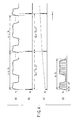
- the optical signal Px actually transmitted on the optical network is not necessarily a repetitive waveform as shown in (a) of FIG. 5 .
- this optical signal Px is sampled with a period Ts equal to N ⁇ Tc+ ⁇ T as shown in (b) of FIG. 5 .
- Ts the period of the optical signal Px
- the value obtained by sampling has an amplitude corresponding to the data “1”, “0” or an amplitude in transition state between the data, as shown in (c) of FIG. 5 . Therefore, the sampling result on the waveform continuous for a predetermined period of the optical signal Px is not obtained.
- the quality value Q can be determined.
- the sampling result for plural bits is superposed over the 1-bit width.
- an eye pattern as shown in (d) of FIG. 5 is obtained, and the signal quality may be determined from this eye pattern.
- the observed waveform obtained by superposition would be deviated and the eye pattern could not be observed.
- FIG. 6 is a block diagram shown for explaining the configuration of the optical signal sync sampling apparatus 100 and the optical signal monitor apparatus 20 ′ using the sampling apparatus 100 according to a second embodiment of the invention.
- FIG. 6 An example of the configuration of the optical signal monitor apparatus 20 ′ always capable of holding the synchronous state is shown in FIG. 6 .
- the sampling light pulse generating unit 21 the optical sampling apparatus 22 , the parameter setting unit 28 , the photoelectric converter 30 and the A/D converter 31 are equivalent to the corresponding component parts of the first embodiment and therefore not described again.
- the output signal Ez of the photoelectric converter 30 is input to the fundamental wave component signal output unit 41 .
- the fundamental wave component signal output unit 41 is for outputting the fundamental wave component signal U having a frequency equal to that of the fundamental wave component of the envelope wave of the signal Ez output in pulse form from the photoelectric converter 30 .
- the fundamental wave component signal output unit 41 may be formed of either a filter type or PLL (phase-locked loop) type.
- the sinusoidal fundamental wave component signal U is extracted by a narrow-band bandpass filter having the central frequency (for RZ scheme) equal to the clock frequency Fc of the data signal modulating the optical signal or the central frequency (for NRZ scheme) twice as high as the clock frequency Fc.
- the output signal of the narrow-band bandpass filter 41 a described above and the output signal of a voltage controlled oscillator 41 b are input to a phase comparator 41 c , and the oscillation frequency of the voltage-controlled oscillator 41 b is controlled by the control signal Vc corresponding to the phase difference between the two output signals.
- the phase of the oscillation output signal is synchronized with the output signal of the bandpass filter 41 a , and this synchronous sinusoidal oscillation output signal is used as the fundamental wave component signal U.
- the output signal Ez of the photoelectric converter 30 is input to a fast Fourier transform (FFT) operation unit for frequency analysis thereby to determine the frequency of the fundamental wave component.
- FFT fast Fourier transform
- the fundamental wave component signal U having a frequency equal to the frequency thus determined is generated and output from a signal generator.
- the clock frequency Fc of the optical signal Px is 10 GHz and the offset time ⁇ T is 0.1 ps
- 1000 sampling sessions are required to obtain the 1-bit waveform data of the optical signal Px.
- the time required for conducting the 1000 sampling sessions with the frequency Fs of about 10 MHz is approximately 0.1 ms. This time is equal to the period of the fundamental wave component of the envelope wave of the signal Ez having the frequency of about 10 kHz.
- the fundamental wave component signal U is input to the comparator 42 and compared with the threshold value Vr preset by a threshold value setter 43 .
- the comparison result is input to a data acquisition control unit 44 .
- the data acquisition control unit 44 based on the output signal of the comparator 42 , writes the data signal Dz of the A/D converter 31 in a waveform memory 45 .
- the operation stands by until the timing when the fundamental wave component signal U exceeds the threshold value Vr upward. This operation is repeated a predetermined number H of times.
- the predetermined number W of the data signal Dz are written at H different plural areas of the waveform memory 45 in the order of the address.
- the arithmetic operation unit 35 ′ calculates the value indicating the quality of the optical signal Px to be monitored, based on the data signal Dz written in the waveform memory 45 .
- the optical signal Px to be monitored is for test operation, for example, and repeatedly modulated in a predetermined code string of a predetermined bit length L as shown in (a) of FIG. 8 , then, as shown in (b) of FIG. 8 , the sampling operation is performed while the value N determining the period Ts of the sampling light pulse Ps is equal to a value K (K: integer) times larger than the bit length L. In this way, as shown in (c) and (d) of FIG. 8 , an optical pulse Pz having an envelope waveform of an enlarged time axis of the optical signal Px is obtained.
- time axis is shown in shorter scale in (d) to (f) of FIG. 8 .
- the waveform data acquisition is started from the timing when the fundamental wave component signal U exceeds the threshold value Vr, so that the process for J bits is executed plural times and stored in different areas 1 to H of the waveform memory 45 as shown in FIG. 9 .
- the head data of these waveform data is equal to a value sampled immediately after the timing when the fundamental wave component signal U exceeds the threshold value Vr and synchronized exactly with the data signal. Therefore, the time axis of the waveform data superposed is not greatly displaced, and the amplitude variation of the optical signal is expressed substantially accurately.
- the relation between the quality and the position in the bit is determined on this eye pattern.
- the value Q is calculated based on the sample value at an intermediate point L (intermediate point of 1 bit) of two cross points as shown in FIG. 10 , and together with the Q value of the whole data irrespective of the position described above, notified to other devices through a communication means not shown.
- the optical signal Px actually transmitted on the optical network is not limited to the repetitive waveform shown in (a) of FIG. 11 .
- this optical signal Px is sampled with the period Ts equal to N ⁇ Tc+ ⁇ T as shown in (b) of FIG. 11 , the sample timing is different by ⁇ T for every N bits of the optical signal Px.
- the peak value of the optical pulse signal Pz obtained by the sampling is either the amplitude corresponding to the data “1”, “0” or the amplitude in the transition state therebetween.
- the envelope wave of an enlarged continuous waveform for a predetermined period of the optical signal Px is not obtained.
- This envelope wave contains the fundamental wave component of the data signal modulating the optical signal Px, and this fundamental wave component signal U is obtained as shown in (e) of FIG. 11 .
- the data acquisition is started as shown in (f) of FIG. 11 at the timing when the fundamental wave component signal U exceeds the threshold value Vr, and the data is acquired by J ⁇ Tc/ ⁇ T times sample sessions (U: integer).
- the Q value can be determined by performing a similar arithmetic operation described above on the J-bit waveform data.
- time axis is shown in shorter scale in (d) to (f) of FIG. 11 .
- This J-bit waveform data itself may be said to indicate the eye pattern.
- the acquisition of the waveform data is started from the timing when the fundamental wave component signal U exceeds the threshold value Vr and conducted for J bits. This process is repeated H times and as in the aforementioned case, stored in different areas 1 to H of the waveform memory 45 . By superposing this data in the order of address, an accurate eye pattern can be obtained.
- the head data of each waveform data has a value sampled immediately after the timing when the fundamental wave component signal U exceeds the threshold value Vr and is accurately synchronized with the data signal.
- the waveform data is not superposed with the time axis greatly displaced, and indicates the amplitude variation of the optical signal in substantially accurate manner.
- the optical sampling unit 22 used for the optical signal monitor apparatus 20 , 20 ′ includes the electroabsorption modulator 24 as a sampling element.
- One of the optical terminals of the modulator 24 is supplied with the multiplexed signal of the optical signal to be sampled and the sampling light pulse.
- the power supply terminal is supplied with a predetermined DC voltage indicating a high absorption rate in the absence of the incident sampling light pulse and a low absorption rate in the presence of the incident sampling light pulse, so that in the presence of the incident sampling light pulse, the component of the optical signal is selectively emitted from the light from the other optical terminal.
- the optical pulse having a narrow width can be used for sampling, and in addition, the loss of the optical signal can be reduced.
- the sampling efficiency is substantively improved, and the accurate waveform information can be obtained even for a weak optical signal.
- the time axis is not likely to be displaced greatly and the eye pattern of the optical signal can be obtained in stable fashion even when the data signals Dz acquired for different periods are superposed.
- the arithmetic operation unit 35 ′ may be done without and the data written in each area of the waveform memory 45 may be transmitted to an external device through a communication means not shown thereby to display the arithmetic operation on the quality and the eye pattern on the particular external device.
- the optical signal Px and the sampling light pulse Ps of different wavelengths are multiplexed with each other and applied to one optical terminal 24 a of the electroabsorption modulator 24 , while the wavelength component of the optical signal is separated and extracted from the light emitted from the other optical terminal 24 b thereby to sample the optical signal.
- the repetitive waveform of the optical signal Px to be monitored is then sampled at time intervals of, for example, ⁇ T in time series as shown in (c) of FIG. 4 .
- the optical signal Px is sampled U ⁇ Tc/ ⁇ T times (U: integer) continuously thereby to obtain the waveform data of U bits in time series from the sampling start timing.
- the time axis of the waveform data finally obtained is calibrated into a state desirable for evaluation of the waveform data.
- this gives rise to the requirement of an expensive sampling light pulse generating unit 21 having a complicated configuration as shown in FIG. 2 .
- an inexpensive sampling light pulse generating unit having a simple configuration may be used in place of the expensive sampling light pulse generating unit 21 having a complicated configuration as shown in FIG. 2 .
- FIG. 12 is a block diagram shown for explaining the configuration of the optical signal sampling apparatus 100 A and the optical signal monitor apparatus 20 A using the apparatus 100 A according to the third embodiment of the invention.
- the optical signal Px to be monitored enters the polarized wave controller 23 a , and the direction of polarization thereof is set orthogonal to the direction of polarization of the sampling light pulse Ps, after which the resulting light, together with the sampling light pulse Ps, is applied to and multiplexed in the optical coupler 23 b of polarization multiplexing type making up the optical combiner 23 .
- the multiplexed light Py′ is applied to one optical terminal 24 a of the electroabsorption modulator 24 , and among the light rays emitted from the other optical terminal 24 b , only the polarized component Pz of the optical signal Px is selected by the polarization filter 26 ′ as an optical separator.
- the sampling light pulse generating unit 21 of this optical signal monitor apparatus 20 A generates the sampling light pulse Ps having the direction of polarization orthogonal to the direction of polarization of the optical signal Px to be monitored.
- any one of the polarization controller, the polarization plate and the polarized beam splitter can be used. Also, as the polarization filter 26 ′, the polarization plate or the polarized beam splitter can be used.
- FIG. 13 is a block diagram shown for explaining the configuration of the optical signal sampling apparatus 100 B and the optical signal monitor apparatus 20 B using the apparatus 100 B according to the fourth embodiment of the invention.
- the sampling light pulse generating unit 21 B making up the optical signal sampling apparatus 100 B shown in FIG. 13 in which the time axis of the waveform data finally obtained is not required to be calibrated, is configured of a short pulse generating unit 21 g which has the function of self-oscillating a short pulse Ps′ having the frequency different by one integer-th from the frequency of the optical signal Px to be sampled on the one hand and shifting the frequency of the short pulse Ps′ by about ⁇ 5% (5 kHz, for example) of the frequency (10 MHz, for example) of the short pulse Ps′ on the other hand.
- This short pulse generating unit 21 g may be, for example, a mode lock fiber laser (MLFL) disclosed in Patent Document 3 described above and can realize an inexpensive sampling light pulse generating unit having a simple configuration.
- MLFL mode lock fiber laser
- this optical signal monitor apparatus 20 B is equivalent to those of the first embodiment shown in FIG. 1 , and therefore, not described again (except that the parameter setting unit 28 is not required).
- FIG. 14 is a block diagram shown for explaining the configuration of the optical signal sampling apparatus 100 C and the optical signal monitor apparatus 20 C using the apparatus 100 C according to the fifth embodiment of the invention.
- the sampling light pulse generating unit 21 C making up the optical signal sampling apparatus 100 C shown in FIG. 14 in which the time axis of the waveform data finally obtained is not required to be calibrated, is configured of a short pulse generating unit 21 g which has the function of self-oscillating a short pulse having the frequency different by one integer-th from the frequency of the optical signal Px to be sampled on the one hand and shifting the frequency of the short pulse on the other hand.
- This short pulse generating unit 21 g may be, for example, a mode lock fiber laser (MLFL) disclosed in Patent Document 3 described above and can realize an inexpensive sampling light pulse generating unit having a simple configuration.
- MLFL mode lock fiber laser
- this optical signal monitor apparatus 20 C is equivalent to those of the second embodiment shown in FIG. 6 , and therefore, not described again (except that the parameter setting unit 28 is not required).
- an optical signal sampling apparatus and method for solving the problems of the prior art, having a high sampling efficiency and capable of sampling the waveform information of a fast optical signal accurately with a sufficient resolution, and an optical signal monitor apparatus and method capable of accurately monitoring the optical signal and obtaining an eye pattern of the optical signal in stable fashion using the optical signal sampling apparatus and method.
Landscapes
- Physics & Mathematics (AREA)
- General Physics & Mathematics (AREA)
- Spectroscopy & Molecular Physics (AREA)
- Photometry And Measurement Of Optical Pulse Characteristics (AREA)
- Optical Modulation, Optical Deflection, Nonlinear Optics, Optical Demodulation, Optical Logic Elements (AREA)
- Optical Communication System (AREA)
Applications Claiming Priority (3)
| Application Number | Priority Date | Filing Date | Title |
|---|---|---|---|
| JP2007138934 | 2007-05-25 | ||
| JP2007-138934 | 2007-05-25 | ||
| PCT/JP2008/059367 WO2008146684A1 (fr) | 2007-05-25 | 2008-05-21 | Dispositif d'échantillonnage de signal optique et son procédé, et dispositif de contrôle optique utilisant ledit dispositif et son procédé |
Publications (2)
| Publication Number | Publication Date |
|---|---|
| US20100232787A1 US20100232787A1 (en) | 2010-09-16 |
| US8050558B2 true US8050558B2 (en) | 2011-11-01 |
Family
ID=40074941
Family Applications (1)
| Application Number | Title | Priority Date | Filing Date |
|---|---|---|---|
| US12/308,264 Expired - Fee Related US8050558B2 (en) | 2007-05-25 | 2008-05-21 | Optical signal sampling apparatus and method and optical signal monitor apparatus and method using the same |
Country Status (5)
| Country | Link |
|---|---|
| US (1) | US8050558B2 (fr) |
| EP (1) | EP2180302A4 (fr) |
| JP (1) | JP5380647B2 (fr) |
| CA (1) | CA2658012A1 (fr) |
| WO (1) | WO2008146684A1 (fr) |
Cited By (1)
| Publication number | Priority date | Publication date | Assignee | Title |
|---|---|---|---|---|
| WO2019084069A1 (fr) * | 2017-10-24 | 2019-05-02 | Drexel University | Sources rf synthétisées hautement stables compactes utilisant des notes de battement verrouillées en mode automatique de lasers multimodes |
Families Citing this family (10)
| Publication number | Priority date | Publication date | Assignee | Title |
|---|---|---|---|---|
| JP5380647B2 (ja) | 2007-05-25 | 2014-01-08 | アンリツ株式会社 | 光信号サンプリング装置及びその方法並びにそれを用いる光信号モニタ装置及びその方法 |
| JP2010193174A (ja) * | 2009-02-18 | 2010-09-02 | Anritsu Corp | 光信号モニタ装置 |
| JP5115990B2 (ja) * | 2009-02-18 | 2013-01-09 | アンリツ株式会社 | 光信号モニタ装置 |
| JP2010204006A (ja) * | 2009-03-05 | 2010-09-16 | Anritsu Corp | 光信号モニタ装置及び該装置のサンプリング周波数調整方法 |
| JP5069265B2 (ja) * | 2009-03-18 | 2012-11-07 | アンリツ株式会社 | 光信号モニタ装置 |
| JP5026454B2 (ja) * | 2009-03-18 | 2012-09-12 | アンリツ株式会社 | 光信号モニタ装置 |
| JP5429763B2 (ja) * | 2013-05-22 | 2014-02-26 | アンリツ株式会社 | 光信号モニタ装置及び該装置のサンプリング周波数調整方法 |
| AT521463B1 (de) * | 2018-10-03 | 2020-02-15 | Ait Austrian Inst Tech Gmbh | Verfahren zur Detektion von Diskontinuitäten in einem optischen Kanal, insbesondere bei einer Glasfaserleitung |
| EP4046246A4 (fr) * | 2019-10-15 | 2023-12-20 | Photonic Systems, Inc. | Système et procédé d'échantillonnage d'impulsions étendues |
| JP7595541B2 (ja) * | 2021-09-01 | 2024-12-06 | 東京エレクトロン株式会社 | プラズマ測定方法 |
Citations (14)
| Publication number | Priority date | Publication date | Assignee | Title |
|---|---|---|---|---|
| JPS62215917A (ja) | 1986-03-18 | 1987-09-22 | Hamamatsu Photonics Kk | 光パルス列に同期した電気信号発生装置 |
| JPH0663869B2 (ja) | 1989-05-29 | 1994-08-22 | 日本電信電話株式会社 | 光サンプリング波形測定装置 |
| JPH08204678A (ja) | 1995-01-26 | 1996-08-09 | Nippon Telegr & Teleph Corp <Ntt> | 時分割多重光信号の多重分離方法及びその装置 |
| JPH08233662A (ja) | 1995-02-28 | 1996-09-13 | Ando Electric Co Ltd | 光パルス波形測定器 |
| JPH1172757A (ja) | 1997-07-04 | 1999-03-16 | Nippon Telegr & Teleph Corp <Ntt> | 光パルス多重装置 |
| US6396601B1 (en) * | 1997-12-01 | 2002-05-28 | Nippon Telegraph And Telephone Corporation | System for monitoring quality of optical signals having different bit rates |
| JP2002368313A (ja) | 2001-06-12 | 2002-12-20 | Aisin Seiki Co Ltd | 受動型モードロック・ファイバーレーザー |
| JP2003344168A (ja) | 2002-05-29 | 2003-12-03 | Ando Electric Co Ltd | 光サンプリング測定装置及び方法 |
| JP2004222252A (ja) | 2002-12-24 | 2004-08-05 | Nec Corp | 光信号モニタ装置、及びその方法 |
| JP2004286511A (ja) | 2003-03-20 | 2004-10-14 | Anritsu Corp | 光サンプリング装置および光波形観測システム |
| JP2005345312A (ja) | 2004-06-03 | 2005-12-15 | Nippon Telegr & Teleph Corp <Ntt> | 光−電気サンプリングによる光信号波形測定・評価装置 |
| WO2008146684A1 (fr) | 2007-05-25 | 2008-12-04 | Anritsu Corporation | Dispositif d'échantillonnage de signal optique et son procédé, et dispositif de contrôle optique utilisant ledit dispositif et son procédé |
| US20090232513A1 (en) * | 2007-01-09 | 2009-09-17 | Akihito Otani | Optical signal synchronization sampling apparatus and method, and optical signal monitoring apparatus and method using the same |
| US20100150548A1 (en) * | 2007-01-15 | 2010-06-17 | Akihito Otani | Optical Signal Quality Monitoring Apparatus and Method |
Family Cites Families (4)
| Publication number | Priority date | Publication date | Assignee | Title |
|---|---|---|---|---|
| JP4659190B2 (ja) * | 2000-08-31 | 2011-03-30 | アンリツ株式会社 | 波形測定装置 |
| JP3876646B2 (ja) * | 2001-05-16 | 2007-02-07 | 三菱電機株式会社 | 光受信器 |
| JP2005070698A (ja) * | 2003-08-28 | 2005-03-17 | National Institute Of Information & Communication Technology | 光パルス分離装置 |
| JP4686272B2 (ja) * | 2005-06-29 | 2011-05-25 | アンリツ株式会社 | サンプリング装置および波形観測システム |
-
2008
- 2008-05-21 JP JP2008550979A patent/JP5380647B2/ja not_active Expired - Fee Related
- 2008-05-21 US US12/308,264 patent/US8050558B2/en not_active Expired - Fee Related
- 2008-05-21 WO PCT/JP2008/059367 patent/WO2008146684A1/fr not_active Ceased
- 2008-05-21 CA CA002658012A patent/CA2658012A1/fr not_active Abandoned
- 2008-05-21 EP EP08753044.0A patent/EP2180302A4/fr not_active Withdrawn
Patent Citations (17)
| Publication number | Priority date | Publication date | Assignee | Title |
|---|---|---|---|---|
| JPS62215917A (ja) | 1986-03-18 | 1987-09-22 | Hamamatsu Photonics Kk | 光パルス列に同期した電気信号発生装置 |
| JPH0663869B2 (ja) | 1989-05-29 | 1994-08-22 | 日本電信電話株式会社 | 光サンプリング波形測定装置 |
| JPH08204678A (ja) | 1995-01-26 | 1996-08-09 | Nippon Telegr & Teleph Corp <Ntt> | 時分割多重光信号の多重分離方法及びその装置 |
| JPH08233662A (ja) | 1995-02-28 | 1996-09-13 | Ando Electric Co Ltd | 光パルス波形測定器 |
| JPH1172757A (ja) | 1997-07-04 | 1999-03-16 | Nippon Telegr & Teleph Corp <Ntt> | 光パルス多重装置 |
| JP3796357B2 (ja) | 1997-12-01 | 2006-07-12 | 日本電信電話株式会社 | 光信号品質モニタ |
| US6396601B1 (en) * | 1997-12-01 | 2002-05-28 | Nippon Telegraph And Telephone Corporation | System for monitoring quality of optical signals having different bit rates |
| JP2002368313A (ja) | 2001-06-12 | 2002-12-20 | Aisin Seiki Co Ltd | 受動型モードロック・ファイバーレーザー |
| US6819689B2 (en) | 2001-06-12 | 2004-11-16 | Aisin Seiki Kabushiki Kaisha | Passive mode lock fiber laser |
| JP2003344168A (ja) | 2002-05-29 | 2003-12-03 | Ando Electric Co Ltd | 光サンプリング測定装置及び方法 |
| JP2004222252A (ja) | 2002-12-24 | 2004-08-05 | Nec Corp | 光信号モニタ装置、及びその方法 |
| US7174098B2 (en) | 2002-12-24 | 2007-02-06 | Nec Corporation | Apparatus and method for monitoring optical signal |
| JP2004286511A (ja) | 2003-03-20 | 2004-10-14 | Anritsu Corp | 光サンプリング装置および光波形観測システム |
| JP2005345312A (ja) | 2004-06-03 | 2005-12-15 | Nippon Telegr & Teleph Corp <Ntt> | 光−電気サンプリングによる光信号波形測定・評価装置 |
| US20090232513A1 (en) * | 2007-01-09 | 2009-09-17 | Akihito Otani | Optical signal synchronization sampling apparatus and method, and optical signal monitoring apparatus and method using the same |
| US20100150548A1 (en) * | 2007-01-15 | 2010-06-17 | Akihito Otani | Optical Signal Quality Monitoring Apparatus and Method |
| WO2008146684A1 (fr) | 2007-05-25 | 2008-12-04 | Anritsu Corporation | Dispositif d'échantillonnage de signal optique et son procédé, et dispositif de contrôle optique utilisant ledit dispositif et son procédé |
Non-Patent Citations (6)
| Title |
|---|
| English language International Search Report dated Jul. 1, 2008, issued in counterpart International Application Serial No. PCT/JP2008/059367. |
| H Zhang, M.Yao,C. Peng, Y.Gao, Opticla waveform measurement with electroabsorption modulator as sampling component, Feb. 2004, Optical engineering vol. 43 No. 2, pp. 441-444. * |
| International Preliminary Report on Patentability dated Jan. 12, 2010 (in English) in parent International Application No. PCT/JP2008/059367. |
| N. Edagawa et al; Wavelength Conversion Using an Electroabsorption Modulator; KDD R&D Laboratories; 1997; p. 727. |
| N.Edagawa, M.Suzuki,S.Yamamoto,S.Akiba, Novel wavelength converter using an electroabsorption modulator:conversion experiments up to 40 Gbit/s OFC Feb. 1997 techical digest, pp. 77-78. * |
| T.Mori, A.Otani, T.Otani, All-optical sampling using cross-absorption modulation in Electroabsorption modulator for optical performance monitor, Sep. 2008, Optical communication 2008 ECOC 34th European conference, pp. 1-2. * |
Cited By (2)
| Publication number | Priority date | Publication date | Assignee | Title |
|---|---|---|---|---|
| WO2019084069A1 (fr) * | 2017-10-24 | 2019-05-02 | Drexel University | Sources rf synthétisées hautement stables compactes utilisant des notes de battement verrouillées en mode automatique de lasers multimodes |
| US11791608B2 (en) | 2017-10-24 | 2023-10-17 | Drexel University | Compact highly-stable synthesized RF sources using self mode-locked beat-notes of multi-modes lasers |
Also Published As
| Publication number | Publication date |
|---|---|
| JPWO2008146684A1 (ja) | 2010-08-19 |
| WO2008146684A1 (fr) | 2008-12-04 |
| EP2180302A1 (fr) | 2010-04-28 |
| JP5380647B2 (ja) | 2014-01-08 |
| CA2658012A1 (fr) | 2008-12-04 |
| EP2180302A4 (fr) | 2014-01-15 |
| US20100232787A1 (en) | 2010-09-16 |
Similar Documents
| Publication | Publication Date | Title |
|---|---|---|
| US8050558B2 (en) | Optical signal sampling apparatus and method and optical signal monitor apparatus and method using the same | |
| US8098995B2 (en) | Optical signal synchronization sampling apparatus and method, and optical signal monitoring apparatus and method using the same | |
| US7010444B2 (en) | Measuring apparatus and measuring method for pattern dependent jitter | |
| US8041211B2 (en) | Optical signal quality monitoring apparatus and method | |
| JP3810570B2 (ja) | 光パルス発生方法及びその装置 | |
| US8019218B2 (en) | Optical signal monitoring apparatus and method | |
| JP2004048688A (ja) | 高速サンプリングによるデータ信号品質評価方法および装置 | |
| Zhou et al. | Linear frequency-modulated waveform generation based on a tunable optoelectronic oscillator | |
| EP1669730A2 (fr) | Analyse spectrale optique basée sur la technique hétérodyne utilisant un échantillonnage par impulsions d'horloge | |
| JP5366139B2 (ja) | 光信号波形計測装置 | |
| KR20110045507A (ko) | 결맞는 빔결합 시 직접잠금 방법을 이용하는 레이저 시스템 | |
| JP2010204106A (ja) | 光サンプリング装置および光信号品質モニタ | |
| JP2008275547A (ja) | 光サンプリング装置および光信号品質モニタ | |
| JP5372447B2 (ja) | サンプリング装置および信号モニタ | |
| Oguchi et al. | Complete analysis of picosecond optical pulses by using the offset frequency intensity modulation | |
| JP4626628B2 (ja) | パルス幅測定装置、パルス幅測定方法、光伝送路分散検出装置及び光伝送路分散検出方法 | |
| JP3286151B2 (ja) | 光サンプリング装置 | |
| Tang et al. | Photonics-Based Microwave Frequency Measurement with Broadband Signal Generation and Processing | |
| JP2002296146A (ja) | 時間応答測定方法および装置 | |
| Xie et al. | Microwave Waveform Generation via Discrete Fourier Transform of Modulated Optical Pulse Train | |
| JP2005192046A (ja) | パルス発生装置および方法 | |
| JP2007036989A (ja) | マルチレートクロック信号抽出方法及びマルチレートクロック信号抽出装置 | |
| JP2005017129A (ja) | 波長分散測定装置 | |
| JP2006041681A (ja) | 試験用光信号発生装置 | |
| JP2003298419A (ja) | 光サンプリング装置 |
Legal Events
| Date | Code | Title | Description |
|---|---|---|---|
| AS | Assignment |
Owner name: ANRITSU CORPORATION, JAPAN Free format text: ASSIGNMENT OF ASSIGNORS INTEREST;ASSIGNORS:OTANI, AKIHITO;TANIMOTO, TAKAO;REEL/FRAME:022005/0650 Effective date: 20081110 |
|
| STCF | Information on status: patent grant |
Free format text: PATENTED CASE |
|
| FEPP | Fee payment procedure |
Free format text: PAYOR NUMBER ASSIGNED (ORIGINAL EVENT CODE: ASPN); ENTITY STATUS OF PATENT OWNER: LARGE ENTITY |
|
| FPAY | Fee payment |
Year of fee payment: 4 |
|
| FEPP | Fee payment procedure |
Free format text: MAINTENANCE FEE REMINDER MAILED (ORIGINAL EVENT CODE: REM.); ENTITY STATUS OF PATENT OWNER: LARGE ENTITY |
|
| LAPS | Lapse for failure to pay maintenance fees |
Free format text: PATENT EXPIRED FOR FAILURE TO PAY MAINTENANCE FEES (ORIGINAL EVENT CODE: EXP.); ENTITY STATUS OF PATENT OWNER: LARGE ENTITY |
|
| STCH | Information on status: patent discontinuation |
Free format text: PATENT EXPIRED DUE TO NONPAYMENT OF MAINTENANCE FEES UNDER 37 CFR 1.362 |
|
| FP | Lapsed due to failure to pay maintenance fee |
Effective date: 20191101 |