US8253473B2 - Integrated circuit of an integrator with enhanced stability and related stabilization method - Google Patents
Integrated circuit of an integrator with enhanced stability and related stabilization method Download PDFInfo
- Publication number
- US8253473B2 US8253473B2 US12/893,908 US89390810A US8253473B2 US 8253473 B2 US8253473 B2 US 8253473B2 US 89390810 A US89390810 A US 89390810A US 8253473 B2 US8253473 B2 US 8253473B2
- Authority
- US
- United States
- Prior art keywords
- transconductance amplifier
- control signal
- voltage
- output
- generate
- Prior art date
- Legal status (The legal status is an assumption and is not a legal conclusion. Google has not performed a legal analysis and makes no representation as to the accuracy of the status listed.)
- Active, expires
Links
- 238000000034 method Methods 0.000 title claims description 13
- 230000006641 stabilisation Effects 0.000 title description 2
- 238000011105 stabilization Methods 0.000 title description 2
- 230000007850 degeneration Effects 0.000 claims 9
- 230000008878 coupling Effects 0.000 claims 4
- 238000010168 coupling process Methods 0.000 claims 4
- 238000005859 coupling reaction Methods 0.000 claims 4
- 238000004519 manufacturing process Methods 0.000 claims 1
- 230000000087 stabilizing effect Effects 0.000 claims 1
- 239000003990 capacitor Substances 0.000 description 3
- 230000010363 phase shift Effects 0.000 description 2
- 230000001419 dependent effect Effects 0.000 description 1
Images




Classifications
-
- H—ELECTRICITY
- H03—ELECTRONIC CIRCUITRY
- H03H—IMPEDANCE NETWORKS, e.g. RESONANT CIRCUITS; RESONATORS
- H03H11/00—Networks using active elements
- H03H11/02—Multiple-port networks
- H03H11/04—Frequency selective two-port networks
- H03H11/0422—Frequency selective two-port networks using transconductance amplifiers, e.g. gmC filters
-
- Y—GENERAL TAGGING OF NEW TECHNOLOGICAL DEVELOPMENTS; GENERAL TAGGING OF CROSS-SECTIONAL TECHNOLOGIES SPANNING OVER SEVERAL SECTIONS OF THE IPC; TECHNICAL SUBJECTS COVERED BY FORMER USPC CROSS-REFERENCE ART COLLECTIONS [XRACs] AND DIGESTS
- Y10—TECHNICAL SUBJECTS COVERED BY FORMER USPC
- Y10T—TECHNICAL SUBJECTS COVERED BY FORMER US CLASSIFICATION
- Y10T29/00—Metal working
- Y10T29/49—Method of mechanical manufacture
- Y10T29/49002—Electrical device making
- Y10T29/49117—Conductor or circuit manufacturing
- Y10T29/49124—On flat or curved insulated base, e.g., printed circuit, etc.
Definitions
- This invention relates to integrated circuit devices, and, more particularly, to an elementary integrator cell having a stable voltage gain.
- Gi tunable transconductance amplifier
- Ci capacitor
- FIG. 1 An exemplary integrator is shown in FIG. 1 .
- the meaning of each block is summarized in the following table:
- the resistance Ri may be the finite output impedance of the transconductance amplifier Gi (due to the finite output impedance of the electronic components constituting the transconductance amplifier) or a resistive element (a resistor or an active device adapted to behave as a resistor) connected at the output of the transconductance amplifier, or a combination of the two.
- the transfer function of the integrator of FIG. 1 is:
- the error amplifier Aio adjusts the gain of the transconductance amplifier Gi and of the matched transconductance amplifier Gmi in order to nullify the difference between the reference current output by the DAC and the current Gmi*Vr of the transconductance amplifier Gmi:
- G mi G DAC R r ( 2 )
- GDAC is the programmable current gain of the digital-to-analog converter.
- the transconductance gain Gmi is adjusted by the control loop for compensating such possible fluctuations, and is tunable by adjusting the gain of the DAC.
- the amplifiers Gi and Gmi When the amplifiers Gi and Gmi are matched, their transconductance may substantially vary according to the same law. However, the transconductance gain Gi and the resistance Ri, and thus also the voltage gain (Gi Ri) of the integrator cell are influenced by process spread, supply voltage, and temperature fluctuations (PVT). This makes the phase of the transfer function of the integrator cell at the crossing frequency fi different from 90°, as it would be in an ideal integrator, and causes a PVT-dependent phase shift. This phase shift may affect the frequency response of filters based on integrator cells, especially if they function at high frequencies and are tunable over a wide frequency range.
- PVT process spread, supply voltage, and temperature fluctuations
- the output resistance of the input transconductance amplifier Gi of the integrator is made independently adjustable from the transconductance gain Gi through a dedicated control signal, and also includes a matched transconductance amplifier Gi 2 having an adjustable gain and an output resistance matched with that of the first transconductance amplifier Gi, and adjusted by the same dedicated control signal.
- a reference current is forced through the matched output resistance, and the dedicated control signal is generated such to keep the output voltage of the matched transconductance amplifier relatively constant.
- a method of stabilization against PVT variations of the integrated circuit of an integrator is also disclosed herein.
- FIG. 1 depicts the architecture of an elementary integrator cell, in accordance with the prior art.
- FIG. 2 depicts an embodiment of the elementary integrator cell of this disclosure.
- FIG. 3 depicts another embodiment of the elementary integrator cell of this disclosure.
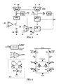
- FIG. 4 depicts yet another embodiment of the elementary integrator cell of this disclosure.
- FIG. 5 depicts yet another embodiment of the elementary integrator cell of this disclosure.
- FIG. 6 depicts a circuit for adjusting the output resistance of FIGS. 3 , 4 , and 5 .
- FIG. 7 depicts an embodiment of a first order LPF employing the elementary integrator cell of this disclosure.
- FIG. 2 A single-end integrator according to a first embodiment is depicted in FIG. 2 .
- the output resistance of the input transconductance amplifier Gi is adjustable through a second control signal Vc, for example by virtue of an adjustable resistive element Ri electrically connected in parallel to the capacitor Ci.
- the cell comprises a second control loop Gi 2 -Rmi-Avo, for example.
- This second control loop includes a co-integrated transconductance amplifier Gi 2 matched with the input transconductance amplifier Gi and having an adjustable output resistance Rmi matched with the output resistance Ri and adjusts the resistances Rmi and Ri in function of the second control signal Vc, in order to keep the voltage on the output of the transconductance amplifier Gi 2 relatively constant.
- This second control loop generates a voltage that varies with fluctuations of the matched resistance Rmi, subtracts it from a constant voltage kVr, and generates the control signal Vc as an amplified replica of the difference with the error voltage amplifier Avo.
- the output resistance Ri is adjusted by the same dedicated control signal.
- the matching between Gi 2 and Gi and between Rmi and Ri fixes the phase of the integrator cell at the 0 dB crossing, independently from PVT induced fluctuations for a large range of frequencies, tunable through the DAC value.
- the output resistance Rmi of the matched transconductance amplifier Gi may be the finite output impedance of the transconductor cell (due to the finite output impedance of the electronic devices making the transconductor cell), a resistive element placed at the output of the transconductor (a resistor or an active device behaving like a resistor), or a combination of the two.
- a reference voltage Vr is applied at the input of the transconductance amplifier Gi to generate an output voltage that will be kept equal to a reference voltage k*Vr by the control loop by the second error amplifier Avo.
- a reference current (Ir) is forced through the matched resistive element Rmi to generate an output voltage (Ir*Rmi) that will be kept equal to a reference voltage k*Vr by the control loop.
- FIGS. 4 and 6 An exemplary embodiment of the adjustable transconductance amplifier Gi and of the matched adjustable resistive element Rmi will now be described.
- an embodiment of the second control loop of the integrator cell realized in differential circuit form is depicted in FIGS. 4 and 6 .
- the transconductance amplifier Gi 2 includes the devices M 1 -M 8 .
- the matched resistive element Rmi includes the devices M 9 -M 11 .
- the NMOS devices M 1 , M 2 may be a differential pair, fed by the input signal Vin+/Vin ⁇ and by the tail current sources M 7 , M 8 .
- tail current sources are not indispensable to realize tail current sources using the depicted MOSFETs M 7 , M 8 and will be immediately capable of identifying in the relevant literature other usable architectures of tail current sources.
- the transistors M 5 , M 6 act as variable degenerating resistors to increase the linearity of the input differential pair. They may be replaced with a short circuit if no linearity improvement is desired, or substituted by other linearization circuitry.
- the PMOS M 3 , M 4 work as an active load.
- the current supplied by M 3 , M 4 is set by a common-mode feedback amplifier CMFB that forces the common mode (Out++Out ⁇ )/2 to match a reference common mode Vcm.
- CMFB common-mode feedback amplifier
- the active load M 3 -M 4 and its relative common mode control may be substituted by any other kind of controlled active loads.
- the finite output resistance of the transconductance amplifier Gmi of FIG. 4 is due to the finite output resistances of the active load M 3 -M 4 and by the finite output resistances of the differential pair M 1 -M 2 .
- the overall output resistance is given by the parallel of the Gmi output resistance and of the Rmi resistance, and it may be adjusted by adjusting the resistance Rmi.
- the adjustable resistance Rmi is realized with the devices M 9 , M 10 , M 11 , that behave as a negative resistance.
- the value of this negative resistance is controlled by the proposed control loop by setting the voltage Vc, that fixes the current flowing through the devices M 9 , M 10 and, as a result, their transconductance.
- variable resistances either positive or negative
- the negative resistance devices have been replaced by the MOS device M 12 that works as a variable positive resistance, controlled by the control voltage Vc.
- FIG. 6 An exemplary embodiment of the circuit that adjusts the resistance is shown in FIG. 6 .
- the transconductance amplifier Gi 2 is input with a null differential voltage.
- a differential reference current Ir is injected into the output node of Gi 2 .
- the differential voltage (Out+ ⁇ Out ⁇ ) is compared with a constant reference kVr to generate the control voltage Vc.
- FIG. 7 shows the two master loops driving a 1st order LPF, whose transfer function A( ⁇ ) is described by the following equation:
- a ⁇ ( ⁇ ) 1 1 + 1 / G i ⁇ R i + j ⁇ ⁇ ⁇ ⁇ ⁇ C i / G i ( 5 )
- Tg ⁇ ( ⁇ ) C i / G i ⁇ ( 1 + 1 / G i ⁇ R i ) 1 + ( ⁇ ⁇ ⁇ C i / G i ⁇ ( 1 + 1 / G i ⁇ R i ) ) 2 ( 6 )
Landscapes
- Networks Using Active Elements (AREA)
- Amplifiers (AREA)
Priority Applications (1)
| Application Number | Priority Date | Filing Date | Title |
|---|---|---|---|
| US13/561,355 US8373488B2 (en) | 2009-10-01 | 2012-07-30 | Integrated circuit of an integrator with enhanced stability and related stabilization method |
Applications Claiming Priority (3)
| Application Number | Priority Date | Filing Date | Title |
|---|---|---|---|
| ITVA20090061 | 2009-10-01 | ||
| ITVA2009A0061 | 2009-10-01 | ||
| ITVA2009A000061 | 2009-10-01 |
Related Child Applications (1)
| Application Number | Title | Priority Date | Filing Date |
|---|---|---|---|
| US13/561,355 Continuation US8373488B2 (en) | 2009-10-01 | 2012-07-30 | Integrated circuit of an integrator with enhanced stability and related stabilization method |
Publications (2)
| Publication Number | Publication Date |
|---|---|
| US20110080218A1 US20110080218A1 (en) | 2011-04-07 |
| US8253473B2 true US8253473B2 (en) | 2012-08-28 |
Family
ID=42729180
Family Applications (2)
| Application Number | Title | Priority Date | Filing Date |
|---|---|---|---|
| US12/893,908 Active 2031-01-07 US8253473B2 (en) | 2009-10-01 | 2010-09-29 | Integrated circuit of an integrator with enhanced stability and related stabilization method |
| US13/561,355 Active US8373488B2 (en) | 2009-10-01 | 2012-07-30 | Integrated circuit of an integrator with enhanced stability and related stabilization method |
Family Applications After (1)
| Application Number | Title | Priority Date | Filing Date |
|---|---|---|---|
| US13/561,355 Active US8373488B2 (en) | 2009-10-01 | 2012-07-30 | Integrated circuit of an integrator with enhanced stability and related stabilization method |
Country Status (3)
| Country | Link |
|---|---|
| US (2) | US8253473B2 (de) |
| EP (1) | EP2306642B1 (de) |
| AT (1) | ATE557472T1 (de) |
Cited By (1)
| Publication number | Priority date | Publication date | Assignee | Title |
|---|---|---|---|---|
| US20140312820A1 (en) * | 2012-12-31 | 2014-10-23 | Silicon Laboratories Inc. | Apparatus for Differencing Comparator and Associated Methods |
Families Citing this family (5)
| Publication number | Priority date | Publication date | Assignee | Title |
|---|---|---|---|---|
| US9819314B1 (en) * | 2017-01-31 | 2017-11-14 | Board Of Regents, The University Of Texas System | Method and circuit for PVT stabilization of dynamic amplifiers |
| US10637422B1 (en) * | 2018-10-31 | 2020-04-28 | Nxp B.V. | Gain compensation for an open loop programmable amplifier for high speed applications |
| US11025212B1 (en) * | 2019-12-20 | 2021-06-01 | Tower Semiconductors Ltd. | Operational transconductance amplifier and a method for converting a differential input voltage to a differential output current |
| CN113157034B (zh) * | 2021-01-19 | 2022-06-03 | 浙江大学 | 一种被动稳压电路实现的高线性度神经形态计算电路 |
| TWI875248B (zh) * | 2023-10-18 | 2025-03-01 | 立積電子股份有限公司 | 放大電路 |
Citations (3)
| Publication number | Priority date | Publication date | Assignee | Title |
|---|---|---|---|---|
| EP0365091A2 (de) | 1988-10-21 | 1990-04-25 | Philips Electronics Uk Limited | Filterschaltungsanordnung |
| EP1578013A2 (de) | 2004-03-16 | 2005-09-21 | Broadcom Corporation | Kalibrierungsschaltung und Verfahren zum Abgleichen der Bandbreite eines Filters |
| US20100141340A1 (en) * | 2008-12-04 | 2010-06-10 | Sun Microsystems, Inc. | Method and apparatus for a high bandwidth amplifier with wide band peaking |
-
2010
- 2010-09-27 EP EP10179881A patent/EP2306642B1/de active Active
- 2010-09-27 AT AT10179881T patent/ATE557472T1/de active
- 2010-09-29 US US12/893,908 patent/US8253473B2/en active Active
-
2012
- 2012-07-30 US US13/561,355 patent/US8373488B2/en active Active
Patent Citations (3)
| Publication number | Priority date | Publication date | Assignee | Title |
|---|---|---|---|---|
| EP0365091A2 (de) | 1988-10-21 | 1990-04-25 | Philips Electronics Uk Limited | Filterschaltungsanordnung |
| EP1578013A2 (de) | 2004-03-16 | 2005-09-21 | Broadcom Corporation | Kalibrierungsschaltung und Verfahren zum Abgleichen der Bandbreite eines Filters |
| US20100141340A1 (en) * | 2008-12-04 | 2010-06-10 | Sun Microsystems, Inc. | Method and apparatus for a high bandwidth amplifier with wide band peaking |
Cited By (2)
| Publication number | Priority date | Publication date | Assignee | Title |
|---|---|---|---|---|
| US20140312820A1 (en) * | 2012-12-31 | 2014-10-23 | Silicon Laboratories Inc. | Apparatus for Differencing Comparator and Associated Methods |
| US10175271B2 (en) * | 2012-12-31 | 2019-01-08 | Silicon Laboratories Inc. | Apparatus for differencing comparator and associated methods |
Also Published As
| Publication number | Publication date |
|---|---|
| US20120286870A1 (en) | 2012-11-15 |
| US8373488B2 (en) | 2013-02-12 |
| US20110080218A1 (en) | 2011-04-07 |
| EP2306642B1 (de) | 2012-05-09 |
| EP2306642A1 (de) | 2011-04-06 |
| ATE557472T1 (de) | 2012-05-15 |
Similar Documents
| Publication | Publication Date | Title |
|---|---|---|
| US8373488B2 (en) | Integrated circuit of an integrator with enhanced stability and related stabilization method | |
| US9473330B1 (en) | Continuous time linear equalizer with a programmable negative feedback amplification loop | |
| US6600373B1 (en) | Method and circuit for tuning a transconductance amplifier | |
| US6335655B1 (en) | Filter circuit | |
| Chen et al. | A systematic realization of third-order quadrature oscillator with controllable amplitude | |
| KR102150503B1 (ko) | 공통 모드 궤환 회로를 포함하는 완전 차동 신호 시스템 | |
| Sotner et al. | First-order adjustable transfer sections for synthesis suitable for special purposes in constant phase block approximation | |
| US5994966A (en) | Transistorized two-port variable-conductance network | |
| Alzaher et al. | A CMOS fully balanced four-terminal floating nullor | |
| US9729126B2 (en) | Method and implementation for accurate gain-bandwidth product tuning | |
| US20060145754A1 (en) | Analog filter circuit and adjustment method thereof | |
| US6621331B2 (en) | Variable negative resistance cell for bipolar integrated circuits | |
| US6791415B2 (en) | Integrated circuit arrangement with a transconductance amplifier | |
| US9948244B1 (en) | Amplifier with adjustable gain | |
| US20020105381A1 (en) | Process-insensitive, highly-linear constant transconductance circuit | |
| US7315199B2 (en) | Q value correction of filter circuit | |
| US7436260B2 (en) | Controlling the ratio of amplification factors between linear amplifiers | |
| US7265609B2 (en) | Transconductor circuits | |
| US7492226B2 (en) | Linearization apparatus of triode region type operational transconductance amplifier | |
| US8120436B2 (en) | System and method for implementing an oscillator | |
| US7345527B2 (en) | Ultra wideband filter based on a pair of cross-coupled transistors | |
| US6933773B2 (en) | Integrated circuit | |
| US20060055463A1 (en) | Linear transconductance cell with wide tuning range | |
| US9871495B2 (en) | Thermal compensation for amplifiers | |
| US20090054004A1 (en) | Biasing for Stacked Circuit Configurations |
Legal Events
| Date | Code | Title | Description |
|---|---|---|---|
| AS | Assignment |
Owner name: STMICROELECTRONICS S.R.L., ITALY Free format text: ASSIGNMENT OF ASSIGNORS INTEREST;ASSIGNORS:ZUFFADA, MAURIZIO;POZZONI, MASSIMO;REEL/FRAME:025234/0266 Effective date: 20100923 |
|
| STCF | Information on status: patent grant |
Free format text: PATENTED CASE |
|
| FPAY | Fee payment |
Year of fee payment: 4 |
|
| MAFP | Maintenance fee payment |
Free format text: PAYMENT OF MAINTENANCE FEE, 8TH YEAR, LARGE ENTITY (ORIGINAL EVENT CODE: M1552); ENTITY STATUS OF PATENT OWNER: LARGE ENTITY Year of fee payment: 8 |
|
| MAFP | Maintenance fee payment |
Free format text: PAYMENT OF MAINTENANCE FEE, 12TH YEAR, LARGE ENTITY (ORIGINAL EVENT CODE: M1553); ENTITY STATUS OF PATENT OWNER: LARGE ENTITY Year of fee payment: 12 |