US8300433B2 - Isolated primary circuit regulator - Google Patents
Isolated primary circuit regulator Download PDFInfo
- Publication number
- US8300433B2 US8300433B2 US12/817,884 US81788410A US8300433B2 US 8300433 B2 US8300433 B2 US 8300433B2 US 81788410 A US81788410 A US 81788410A US 8300433 B2 US8300433 B2 US 8300433B2
- Authority
- US
- United States
- Prior art keywords
- signal
- discharge time
- switch
- switching
- transformer
- Prior art date
- Legal status (The legal status is an assumption and is not a legal conclusion. Google has not performed a legal analysis and makes no representation as to the accuracy of the status listed.)
- Active, expires
Links
- 230000010355 oscillation Effects 0.000 claims abstract description 14
- 239000003990 capacitor Substances 0.000 claims description 14
- 238000001914 filtration Methods 0.000 claims description 8
- 238000012545 processing Methods 0.000 claims description 5
- 230000003321 amplification Effects 0.000 claims description 3
- 238000003199 nucleic acid amplification method Methods 0.000 claims description 3
- 230000003139 buffering effect Effects 0.000 claims 1
- 230000000087 stabilizing effect Effects 0.000 abstract 1
- 238000001514 detection method Methods 0.000 description 21
- 230000000875 corresponding effect Effects 0.000 description 13
- 238000010586 diagram Methods 0.000 description 5
- 238000004804 winding Methods 0.000 description 5
- 230000001276 controlling effect Effects 0.000 description 4
- 238000013461 design Methods 0.000 description 3
- 230000007423 decrease Effects 0.000 description 2
- 238000005516 engineering process Methods 0.000 description 2
- 238000004519 manufacturing process Methods 0.000 description 2
- 230000010363 phase shift Effects 0.000 description 2
- 238000005070 sampling Methods 0.000 description 2
- 230000001360 synchronised effect Effects 0.000 description 2
- 230000005540 biological transmission Effects 0.000 description 1
- 238000012937 correction Methods 0.000 description 1
- 230000002596 correlated effect Effects 0.000 description 1
- 238000002474 experimental method Methods 0.000 description 1
- 238000000034 method Methods 0.000 description 1
- 238000011160 research Methods 0.000 description 1
Images



Classifications
-
- H—ELECTRICITY
- H02—GENERATION; CONVERSION OR DISTRIBUTION OF ELECTRIC POWER
- H02M—APPARATUS FOR CONVERSION BETWEEN AC AND AC, BETWEEN AC AND DC, OR BETWEEN DC AND DC, AND FOR USE WITH MAINS OR SIMILAR POWER SUPPLY SYSTEMS; CONVERSION OF DC OR AC INPUT POWER INTO SURGE OUTPUT POWER; CONTROL OR REGULATION THEREOF
- H02M3/00—Conversion of DC power input into DC power output
- H02M3/22—Conversion of DC power input into DC power output with intermediate conversion into AC
- H02M3/24—Conversion of DC power input into DC power output with intermediate conversion into AC by static converters
- H02M3/28—Conversion of DC power input into DC power output with intermediate conversion into AC by static converters using discharge tubes with control electrode or semiconductor devices with control electrode to produce the intermediate AC
- H02M3/325—Conversion of DC power input into DC power output with intermediate conversion into AC by static converters using discharge tubes with control electrode or semiconductor devices with control electrode to produce the intermediate AC using devices of a triode or a transistor type requiring continuous application of a control signal
- H02M3/335—Conversion of DC power input into DC power output with intermediate conversion into AC by static converters using discharge tubes with control electrode or semiconductor devices with control electrode to produce the intermediate AC using devices of a triode or a transistor type requiring continuous application of a control signal using semiconductor devices only
- H02M3/33507—Conversion of DC power input into DC power output with intermediate conversion into AC by static converters using discharge tubes with control electrode or semiconductor devices with control electrode to produce the intermediate AC using devices of a triode or a transistor type requiring continuous application of a control signal using semiconductor devices only with automatic control of the output voltage or current, e.g. flyback converters
- H02M3/33523—Conversion of DC power input into DC power output with intermediate conversion into AC by static converters using discharge tubes with control electrode or semiconductor devices with control electrode to produce the intermediate AC using devices of a triode or a transistor type requiring continuous application of a control signal using semiconductor devices only with automatic control of the output voltage or current, e.g. flyback converters with galvanic isolation between input and output of both the power stage and the feedback loop
Definitions
- the present invention relates to an isolated primary circuit regulator, and more particularly to an isolated primary circuit regulator having a control circuit.
- a power supply In current electronic devices, in order to meet the safety requirements, a power supply is required to be capable of providing a stable output voltage and a stable output current. Under such conditions, the power supply is mostly composed of a transformer, and a switching regulator is disposed at a primary side of the transformer to adjust the output current.
- the technology of disposing the switching regulator at the primary side of the transformer still cannot accurately control the output current of the power supply. Therefore, an additional current loop is required at a secondary side of the power supply, so as to achieve a constant current curve with linear characteristics. As a result, the manufacturing cost is greatly increased. Therefore, how to accurately control the output current of the power supply while reducing the cost is indeed a research subject of interest.
- the method of adjusting the output current of the power supply by disposing the switching regulator at the primary side of the transformer is characterized by detecting a primary-side switching voltage signal and a discharge time of a secondary-side switching current.
- the primary-side switching voltage signal is generated at the primary side of the transformer
- the secondary-side switching current is generated at the secondary side of the transformer.
- ROC Patent No. I277852 discloses a switching control circuit controlling output current at the primary side of a power converter, including as follows:
- a waveform detector generates a current-waveform signal.
- a discharge-time detector detects a discharge-time of a secondary side switching current.
- An oscillator generates an oscillation signal for determining the switching frequency of the switching signal.
- An integrator generates an integrated signal by integrating an average current signal with the discharge-time.
- the average current signal is generated in response to the current-waveform signal.
- the time constant of the integrator is correlated with the switching period of the switching signal, therefore the integrated signal is proportional to the output current.
- An error amplifier amplifies the integrated signal and provides a loop gain for output current control.
- a comparator controls the pulse width of the switching signal in reference to the output of the error amplifier.
- the present invention is an isolated primary circuit regulator, applied to a primary side of a transformer of a power supply.
- the isolated primary circuit regulator comprises a discharge time detector, an oscillator, a pulse width modulator, and a control circuit.
- the discharge time detector is connected to the transformer. It is used for detecting a discharge time of a switching current generated at a secondary side of the transformer, and outputting a discharge time signal and an inverse discharge time signal.
- the control circuit has an input terminal connected to the discharge time detector, and is used for performing signal processing of output current waveform reconstruction, filtering, amplification and comparison on a critical voltage according to the discharge time signal and the inverse discharge time signal, and outputting an adjustment signal.
- the critical voltage is corresponding to a peak value of a switching voltage signal generated at the primary side of the transformer.
- the oscillator is used for generating an oscillation signal.
- a first input terminal and a second input terminal of the pulse width modulator are respectively connected to the control circuit and the oscillator.
- the pulse width modulator is used for receiving the oscillation signal and the adjustment signal, and outputting a switching signal accordingly.
- the switching signal has a duty cycle and a frequency corresponding to the oscillation signal and the adjustment signal, and the adjustment signal is used for resetting the pulse width modulator.
- the isolated primary circuit regulator of the present invention can switch the transformer by using the switching signal to stabilize and to adjust the output current of the power supply. Moreover, the isolated primary circuit regulator of the present invention further uses the control circuit to replace the conventional waveform detector and integrator. Therefore, the isolated primary circuit regulator of the present invention does not directly detect the switching voltage signal generated at the primary side of the transformer, but indirectly obtains the equivalent critical voltage through the feedback design of the control circuit. The isolated primary circuit regulator of the present invention not only can stabilize and adjust the output current of the power supply, but further prevent the false determination due to the voltage spike caused by sudden switching of a switch.
- FIG. 1 is a schematic view of an isolated primary circuit regulator disposed in a power supply according to the present invention
- FIG. 2 is a schematic view of an isolated primary circuit regulator according to an embodiment of the present invention.
- FIG. 3 is a diagram depicting signal waveforms during operation of the power supply of FIG. 1 ;
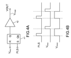
- FIG. 4A is a schematic view of a pulse width modulator according to an embodiment of the present invention.
- FIG. 4B is a diagram depicting signal waveforms of a pulse width modulator according to an embodiment of the present invention.
- FIG. 5 is a schematic view of an output current waveform reconstruction circuit according to an embodiment of the present invention.
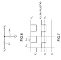
- FIG. 6 is a schematic view of a low-pass filter according to an embodiment of the present invention.
- FIG. 7 is a diagram depicting signal waveforms of a control circuit according to an embodiment of the present invention.
- FIG. 1 is a schematic view of an isolated primary circuit regulator 20 disposed in a power supply according to an embodiment of the present invention.
- the isolated primary circuit regulator 20 is applied to a primary side of a transformer 10 of a power supply.
- the power supply has an input voltage V in , an output voltage V o , and an output current I o .
- the power supply comprises the transformer 10 , and the transformer 10 has an auxiliary winding N A , a primary-side winding N P and a secondary-side winding N S .
- the primary side is defined as a side reference to exactly the same ground level of the input voltage V in
- the secondary side is defined as a side reference to exactly the same ground level of the output voltage V o .
- the isolated primary circuit regulator 20 comprises a power supply terminal VDD, a ground terminal GND, an output terminal VOUT, a discharge time detection terminal VDET and a switching voltage sensing terminal VS.
- the power supply terminal VDD is connected to one terminal of a capacitor 60 , and the other terminal of the capacitor 60 is grounded in the primary side.
- a node between the power supply terminal VDD and the capacitor 60 is connected to the auxiliary winding N A through a rectifier 50 .
- the ground terminal GND is grounded.
- the output terminal VOUT is connected to a gate terminal of a transistor 30 .
- the discharge time detection terminal VDET is connected to the auxiliary winding N A through an auxiliary resistor 40 .
- the switching voltage sensing terminal VS is disposed between a source terminal of the transistor 30 and a detection resistor R S .
- the detection resistor R S is used for connecting the source terminal of the transistor 30 to the ground.
- the isolated primary circuit regulator 20 detects a reflected voltage V W through the discharge time detection terminal VDET, and detects a primary-side switching voltage signal V cs corresponding to a primary-side switching current I P generated at the primary side of the transformer through the switching voltage sensing terminal VS, generates a switching signal V PWM according to the reflected voltage V W and the primary-side switching voltage signal V cs , and outputs the generated switching signal V PWM through the output terminal VOUT.
- the isolated primary circuit regulator 20 switches the transistor 30 by using the switching signal V PWM , so as to control the switching operation of the transformer 10 .
- the primary-side switching voltage signal V cs may be a magnetizing current signal.
- the reflected voltage V W further charges the capacitor 60 through the rectifier 50 , such that the reflected voltage V W supplies energy to the isolated primary circuit regulator 20 .
- the transistor 30 When the switching signal V PWM is at a high level, the transistor 30 is turned on, and the transistor 30 conducts the primary-side switching current I P .
- the switching signal V PWM When the switching signal V PWM is switched to a low level, the energy stored in the transformer 10 is released to the secondary side of the transformer 10 , and is transmitted to an output terminal of the power supply through a rectifier 70 .
- the transistor 30 When the transistor 30 is turned on, the transistor 30 conducts the primary-side switching current I P at the primary side of the transformer.
- the primary-side switching current I P is converted into the primary-side switching voltage signal V cs by the detection resistor R S , and through the switching voltage sensing terminal VS, the primary-side switching voltage signal V cs is detected.
- the primary-side switching current I P increases with the conduction time of the transistor 30 , and reaches a maximum primary-side switching current I pk .
- the voltage value of the primary-side switching voltage signal V cs also increases with the conduction time of the transistor 30 , and eventually reaches a critical voltage V e .
- the critical voltage V e is a peak value of the primary-side switching voltage signal V cs .
- the detection resistor R S has a fixed resistance, and the critical voltage V e is directly proportional to the maximum primary-side switching current I pk , as expressed in Equation (1).
- V e I pk *R S (1)
- the isolated primary circuit regulator 20 may comprise a discharge time detector 22 , an oscillator 24 , a pulse width modulator 26 and a control circuit 28 disposed therein.
- An input terminal of the discharge time detector 22 is connected to the discharge time detection terminal VDET.
- An output terminal of the discharge time detector 22 is connected to an input terminal of the control circuit 28 .
- a first input terminal and a second input terminal of the pulse width modulator 26 are respectively connected to the control circuit 28 and the oscillator 24 .
- the pulse width modulator 26 is used for outputting the switching signal V PWM , and the switching signal V PWM is connected to a gate terminal of the transistor 30 through the output terminal VOUT.
- the discharge time detector 22 detects the reflected voltage V W through the discharge time detection terminal VDET, and thus provides a discharge time signal V dis and an inverse discharge time signal V disB to the control circuit 28 .
- the discharge time signal V dis and the inverse discharge time signal V disB possess opposite phases.
- a secondary-side switching current I s is formed at the secondary side of the transformer, and the reflected voltage V W is hereby generated at the primary side of the transformer in response to the secondary-side switching current I s .
- the secondary-side switching current I s has a maximum secondary-side switching current I spk .
- the secondary-side switching current I s gradually decreases as the discharge period proceeds, and the secondary-side switching current I s eventually drops to zero, causing the reflected voltage V W to drop simultaneously.
- the maximum secondary-side switching current I spk is directly proportional to the maximum primary-side switching current I pk , as expressed in Equation (2).
- I spk I pk *N P /N S (2)
- FIG. 3 is a diagram depicting waveforms measured in experiments according to an embodiment of the present invention.
- a discharge time t disc of the secondary-side switching current I s can be calculated according to the time span starting from the instance when the switching signal V PWM is switched to a low level to the instance when the secondary side switching current I s drops to zero.
- the discharge time detector 22 Since the discharge time detector 22 detects the secondary-side switching current I s (by receiving the reflected voltage V W ) through the discharge time detection terminal VDET, the discharge time detector 22 can obtain the discharge time t disc of the secondary-side switching current I s by calculating the time span starting from the instance when the switching signal V PWM is switched to a low level to the instance when the secondary side switching current I s drops to zero. Therefore, the discharge time detector 22 can effectively detect the discharge time t disc .
- the oscillator 24 is used for generating an oscillation signal (or a clock signal) PLS.
- An input terminal of the control circuit 28 is connected to the discharge time detector 22 .
- the control circuit 28 receives the discharge time signal V dis and the inverse discharge time signal V disB corresponding to the discharge time t disc through such a connection.
- the control circuit 28 performs signal processing of output current waveform reconstruction, filtering, amplification and comparison on the critical voltage V e according to the discharge time signal V dis , the inverse discharge time signal V disB and the switching signal V PWM so as to output an adjustment signal V Mod .
- the pulse width modulator 26 receives the adjustment signal V Mod from the control circuit 28 and the oscillation signal PLS from the oscillator 24 respectively through the first input terminal and the second input terminal.
- the pulse width modulator 26 comprises an SR latch 41 and a gate driver 42 .
- the gate driver 42 is connected to an output terminal of the SR latch 41 .
- the SR latch 41 performs signal processing according to the oscillation signal PLS and the adjustment signal V Mod , and then the gate driver 42 outputs the switching signal V PWM .
- the switching signal V PWM possesses a duty cycle and a frequency corresponding to the oscillation signal PLS and the adjustment signal V Mod , and the adjustment signal V Mod is used for resetting the pulse width modulator 26 .
- the oscillation signal PLS is used for determining when the switching signal V PWM is switched to the high level
- the adjustment signal V Mod is used for determining when the switching signal V PWM is switched to the low level.
- the control circuit 28 comprises an output current waveform reconstruction circuit 100 , a low-pass filter 200 , an error amplifier 300 and a comparator 400 .
- the output current waveform reconstruction circuit 100 is used for sampling and holding the critical voltage V e according to the switching signal V PWM , the discharge time signal V dis and the inverse discharge time signal V disB , so as to reconstruct a current waveform which is corresponding to twice the current waveform of the output current I o occurred at the secondary side After performing correction using a corresponding coefficient, the output current waveform reconstruction circuit 100 finally outputs a square wave signal V a .
- the square wave signal V a has an amplitude corresponding to the critical voltage V e , the square wave signal V a is synchronized to the discharge time signal V dis , and the square wave signal V a has a waveform corresponding to a waveform of the output current I o .
- the low-pass filter 200 is connected to the output current waveform reconstruction circuit 100 .
- the low-pass filter 200 is used for filtering the square wave signal V a , so as to output a direct current (DC) signal V b .
- a negative input terminal of the error amplifier 300 is connected to the DC signal V b .
- a positive input terminal of the error amplifier 300 is connected to a reference voltage V ref .
- the error amplifier 300 is used for amplifying a difference between the DC signal V b and the reference voltage V ref , and the error amplifier 300 outputs the critical voltage V e .
- the reference voltage V ref is preset according to the output current I o . For example, when the output current I o is 0.7 A, the reference voltage V ref may be set to 0.7 V.
- the critical voltage V e output by the error amplifier 300 is fed back to an input terminal of the output current waveform reconstruction circuit 100 .
- the output current waveform reconstruction circuit 100 can receive a voltage equivalent to the primary-side switching voltage signal V cs , thereby preventing false determination of a switching regulator caused by sudden switching of a switch.
- the comparator 400 is connected between the error amplifier 300 and the pulse width modulator 26 .
- the comparator 400 is used for comparing the critical voltage V e to the primary-side switching voltage signal V cs , and the comparator 400 outputs the adjustment signal V mod .
- the output current waveform reconstruction circuit 100 comprises a first switch 101 , a second switch 102 , a third switch 103 , a first capacitor 104 and a buffer 105 .
- the first switch 101 is connected to the critical voltage V e
- the second switch 102 is connected in series with the first switch 101 .
- the third switch 103 is connected to the second switch 102 , and connected in parallel with the first switch 101 and the second switch 102 .
- the first capacitor 104 is connected to a first node between the first switch 101 and the second switch 102 .
- the buffer 105 is connected to a second node between the second switch 102 and the third switch 103 .
- a first detection terminal V g is provided between the first switch 101 and the second switch 102 .
- a second detection terminal V f is provided.
- the switching signal V PWM is used for controlling the first switch 101 .
- the discharge time signal V dis is used for controlling the second switch 102 .
- the inverse discharge time signal V disB is used for controlling the third switch 103 .
- a time interval during which the switching signal V PWM is at the high level as a high-level time interval t on .
- the switching signal V PWM is at the high level
- the discharge time signal V dis is at the low level
- the inverse discharge time signal V disB is at the high level.
- the switching signal V PWM is switched to the low level. Accordingly, the energy originally stored in the transformer 10 is released to the secondary side of the transformer 10 , and the secondary-side switching current I s is hereby generated. As the energy is released to the secondary side of the transformer 10 , the secondary-side switching current I s gradually decreases and eventually drops to zero. Therefore, it is defined that, a time interval from the instance when the switching signal V PWM is switched to the low level to the instance when the secondary-side switching current I s drops to zero as the discharge time t disc . During the time interval of the discharge time t dis , the switching signal V PWM is at the low level, the discharge time signal V dis is at the high level, and the inverse discharge time signal V disB is at the low level.
- a time interval from the instance when the switching signal V PWM is still at the low level and the secondary-side switching current I s drops to zero to the instance when the switching signal V PWM is again switched to the high level is defined as a low-level time interval t disf .
- the switching signal V PWM is at the low level
- the discharge time signal V dis is at the low level
- the inverse discharge time signal V disB is at the high level.
- T t on +t disc +t disf .
- the output current waveform reconstruction circuit 100 has an input terminal for receiving the critical voltage V e output and fed back by the output of the error amplifier 300 .
- the switching signal V PWM is at the high level
- the discharge time signal V dis is at the low level
- the inverse discharge time signal V disB is at the high level. Therefore, the first switch 101 and the third switch 103 are switched off, and the second switch 102 is switched on.
- the value of the critical voltage V e is transmitted to and stored in the first capacitor 104
- the voltage value of the first detection terminal V g is corresponding to the critical voltage V e
- the second detection terminal V f is grounded.
- the switching signal V PWM is switched to the low level, and the output current waveform reconstruction circuit 100 starts to operate at the onset of the time interval of the discharge time t disc .
- the switching signal V PWM is at the low level
- the discharge time signal V dis is at the high level
- the inverse discharge time signal V disB is at the low level. Therefore, the first switch 101 and the third switch 103 are switched on, and the second switch 102 is switched off. Accordingly, the previous voltage of the first detection terminal V g (that is, the critical voltage V e ) is transmitted to the second detection terminal V f .
- the second detection terminal V f detects a buffer signal V a′ that has an amplitude equal to the critical voltage V e and occurs in synchronization to the discharge time signal V dis .
- the buffer 105 is used for adjusting the buffer signal V a′ and outputting the square wave signal V a .
- FIG. 7 is a diagram showing waveforms of the buffer signal V a′ and the square wave signal V a .
- V a the amplitude of the square wave signal V a is adjusted to V e *(N P /N S )/(2*K).
- the output current waveform reconstruction circuit 100 still operates in the low-level time interval t disf .
- the switching signal V PWM is at the low level
- the discharge time signal V dis is at the low level
- the inverse discharge time signal V disB is at the high level. Therefore, the first switch 101 and the second switch 102 are switched on, and the third switch 103 is switched off.
- the first detection terminal V g fails to detect any signal, and the second detection terminal V f is grounded.
- the output current waveform reconstruction circuit 100 repeatedly performs signal processing of sampling and holding and phase shift on the critical voltage V e , and finally the output current waveform reconstruction circuit 100 outputs a square wave signal V a that has an amplitude corresponding to the critical voltage V e and occurs in synchronization to the discharge time signal V dis .
- the square wave signal V a has a waveform corresponding to a waveform of the output current I o . That is to say, the output current waveform reconstruction circuit 100 can be used for reproducing a waveform corresponding to the output current I o .
- the low-pass filter 200 comprises a first resistor 201 and a second capacitor 202 .
- the first resistor 201 is connected between the output current waveform reconstruction circuit 100 and the error amplifier 300 .
- the first resistor 201 is used for receiving the square wave signal V a .
- the second capacitor 202 is connected to a node between the first resistor 201 and the error amplifier 300 . Since the second capacitor 202 has a reactance function and is connected in parallel with the output current waveform reconstruction circuit 100 , the second capacitor 202 can be used for filtering out high-frequency components of the square wave signal V a .
- the low-pass filter 200 can be used for filtering out the high-frequency components of the square wave signal V a and outputting a DC signal V b based on the properties of the first resistor and the second capacitor.
- Equation (3) may be modified to Equation (4) below.
- I o ( N P /N S )*( V e *t disc /R S )/(2 *T ) (4)
- Equation (4) the output current I o of the power supply can be stabilized and adjusted by the isolated primary circuit regulator.
- the isolated primary circuit regulator of the present invention can switch the transformer by using the switching signal, stabilize and adjust the output current of the power supply. Moreover, the isolated primary circuit regulator of the present invention further uses the control circuit having the feedback design to replace the conventional waveform detector and integrator. Therefore, the isolated primary circuit regulator of the present invention does not directly detect the switching voltage signal generated at the primary side of the transformer, but indirectly obtains the equivalent critical voltage. Thus, the isolated primary circuit regulator according to an embodiment of the present invention not only can stabilize and adjust the output current of the power supply, but can further prevent voltage spike caused by sudden switching of a switch.
Landscapes
- Engineering & Computer Science (AREA)
- Power Engineering (AREA)
- Dc-Dc Converters (AREA)
Applications Claiming Priority (3)
| Application Number | Priority Date | Filing Date | Title |
|---|---|---|---|
| TW099110457A TWI379496B (en) | 2010-04-02 | 2010-04-02 | Isolated primary side regulator |
| TW099110457 | 2010-04-02 | ||
| TW99110457A | 2010-04-02 |
Publications (2)
| Publication Number | Publication Date |
|---|---|
| US20110242859A1 US20110242859A1 (en) | 2011-10-06 |
| US8300433B2 true US8300433B2 (en) | 2012-10-30 |
Family
ID=44121707
Family Applications (1)
| Application Number | Title | Priority Date | Filing Date |
|---|---|---|---|
| US12/817,884 Active 2031-07-19 US8300433B2 (en) | 2010-04-02 | 2010-06-17 | Isolated primary circuit regulator |
Country Status (6)
| Country | Link |
|---|---|
| US (1) | US8300433B2 (pl) |
| EP (1) | EP2372891B1 (pl) |
| KR (1) | KR101154382B1 (pl) |
| ES (1) | ES2617204T3 (pl) |
| PL (1) | PL2372891T3 (pl) |
| TW (1) | TWI379496B (pl) |
Cited By (1)
| Publication number | Priority date | Publication date | Assignee | Title |
|---|---|---|---|---|
| US20170149338A1 (en) * | 2015-11-23 | 2017-05-25 | Sync Power Corp. | Regulating power converter by sensing transformer discharge timing |
Families Citing this family (4)
| Publication number | Priority date | Publication date | Assignee | Title |
|---|---|---|---|---|
| US9159450B2 (en) * | 2012-03-21 | 2015-10-13 | System General Corp. | Sampling circuit for measuring reflected voltage of transformer for power converter operated in DCM and CCM |
| TWI488414B (zh) * | 2012-10-30 | 2015-06-11 | Lite On Technology Corp | 具初級側回授控制之返馳式電壓轉換器及其電壓控制方法 |
| US9093910B1 (en) * | 2014-02-14 | 2015-07-28 | Maxim Integrated Products, Inc. | Predictive sampling for primary side sensing in isolated flyback converters |
| US10158296B1 (en) * | 2018-04-18 | 2018-12-18 | Nxp B.V. | Method and system for saturation control in a flyback switched-mode power supply (SMPS) |
Citations (5)
| Publication number | Priority date | Publication date | Assignee | Title |
|---|---|---|---|---|
| US5717578A (en) * | 1996-02-07 | 1998-02-10 | Emerging Technologies Corporation | Constant current source employing power conversion circuitry |
| US6977824B1 (en) * | 2004-08-09 | 2005-12-20 | System General Corp. | Control circuit for controlling output current at the primary side of a power converter |
| TWI277852B (en) | 2005-03-28 | 2007-04-01 | System General Corp | A switching control circuit for controlling output current at the primary side of a power converter |
| US20080007977A1 (en) * | 2006-07-07 | 2008-01-10 | Johan Piper | Switch mode power supply systems |
| US7558093B1 (en) * | 2005-11-10 | 2009-07-07 | Iwatt Inc. | Power converter with emulated peak current mode control |
Family Cites Families (9)
| Publication number | Priority date | Publication date | Assignee | Title |
|---|---|---|---|---|
| US6836415B1 (en) | 2003-06-18 | 2004-12-28 | Systems General Corp. | Primary-side regulated pulse width modulation controller with improved load regulation |
| US7054170B2 (en) | 2004-01-05 | 2006-05-30 | System General Corp. | Power-mode controlled power converter |
| CN1727852A (zh) | 2004-07-26 | 2006-02-01 | 德技股份有限公司 | 超音波雾化器的检测电路 |
| US7362593B2 (en) * | 2004-09-16 | 2008-04-22 | System General Corp. | Switching control circuit having off-time modulation to improve efficiency of primary-side controlled power supply |
| KR101040159B1 (ko) * | 2005-10-09 | 2011-06-09 | 시스템 제너럴 코퍼레이션 | 1차측 제어 파워 변환기들을 위한 가변 스위칭 주파수를갖는 스위칭 제어 회로 |
| JP4763055B2 (ja) * | 2005-10-09 | 2011-08-31 | システム ジェネラル コーポレイション | オフ時間変調を有して一次側制御電源の効率を改善するスイッチング制御回路 |
| KR100920470B1 (ko) * | 2006-11-01 | 2009-10-08 | 박찬웅 | 자기에너지전달소자의 권선 전압으로부터 출력 전류의정보를 검출하는 회로 및 출력 전류를 피드백하는 회로 및프라이머리 피드백에 의해 출력 전류를 제한하는에스엠피에스 |
| US7349229B1 (en) * | 2006-12-20 | 2008-03-25 | System General Corp. | Causal sampling circuit for measuring reflected voltage and demagnetizing time of transformer |
| EP2135347A1 (en) * | 2007-03-23 | 2009-12-23 | System General Corp. | Primary-side controlled switching regulator |
-
2010
- 2010-04-02 TW TW099110457A patent/TWI379496B/zh active
- 2010-06-17 US US12/817,884 patent/US8300433B2/en active Active
- 2010-06-23 EP EP10166996.8A patent/EP2372891B1/en active Active
- 2010-06-23 PL PL10166996T patent/PL2372891T3/pl unknown
- 2010-06-23 ES ES10166996.8T patent/ES2617204T3/es active Active
- 2010-06-29 KR KR1020100061769A patent/KR101154382B1/ko active Active
Patent Citations (5)
| Publication number | Priority date | Publication date | Assignee | Title |
|---|---|---|---|---|
| US5717578A (en) * | 1996-02-07 | 1998-02-10 | Emerging Technologies Corporation | Constant current source employing power conversion circuitry |
| US6977824B1 (en) * | 2004-08-09 | 2005-12-20 | System General Corp. | Control circuit for controlling output current at the primary side of a power converter |
| TWI277852B (en) | 2005-03-28 | 2007-04-01 | System General Corp | A switching control circuit for controlling output current at the primary side of a power converter |
| US7558093B1 (en) * | 2005-11-10 | 2009-07-07 | Iwatt Inc. | Power converter with emulated peak current mode control |
| US20080007977A1 (en) * | 2006-07-07 | 2008-01-10 | Johan Piper | Switch mode power supply systems |
Cited By (2)
| Publication number | Priority date | Publication date | Assignee | Title |
|---|---|---|---|---|
| US20170149338A1 (en) * | 2015-11-23 | 2017-05-25 | Sync Power Corp. | Regulating power converter by sensing transformer discharge timing |
| US9735687B2 (en) * | 2015-11-23 | 2017-08-15 | Sync Power Corp. | Regulating power converter by sensing transformer discharge timing |
Also Published As
| Publication number | Publication date |
|---|---|
| PL2372891T3 (pl) | 2017-06-30 |
| KR101154382B1 (ko) | 2012-06-15 |
| ES2617204T3 (es) | 2017-06-15 |
| US20110242859A1 (en) | 2011-10-06 |
| EP2372891A2 (en) | 2011-10-05 |
| KR20110111210A (ko) | 2011-10-10 |
| TW201136110A (en) | 2011-10-16 |
| TWI379496B (en) | 2012-12-11 |
| EP2372891B1 (en) | 2016-12-28 |
| EP2372891A3 (en) | 2011-11-16 |
Similar Documents
| Publication | Publication Date | Title |
|---|---|---|
| TWI481141B (zh) | And a system and method for protecting a power supply conversion system based at least on a feedback signal | |
| US8971062B2 (en) | Systems and methods for constant voltage mode and constant current mode in flyback power converters with primary-side sensing and regulation | |
| US10277132B2 (en) | Systems and methods for constant voltage mode and constant current mode in flyback power converters with primary-side sensing and regulation | |
| TWI483524B (zh) | A system and method for adjusting a power conversion system | |
| US10205395B2 (en) | Systems and methods for current control of power conversion systems | |
| US10447148B2 (en) | DC/DC resonant converters and power factor correction using resonant converters, and corresponding control methods | |
| US9154039B2 (en) | Switching power converter with secondary-side dynamic load detection and primary-side feedback and control | |
| CN100525038C (zh) | 电源转换器的输出电流控制电路以及电源检测电路 | |
| US7859862B2 (en) | Apparatus and method for regulating constant output voltage and current on primary side in a flyback converter | |
| US7061780B2 (en) | Switching control circuit with variable switching frequency for primary-side-controlled power converters | |
| TWI530078B (zh) | Control circuit and method of fly - back power converter | |
| TWI277279B (en) | Control circuit and control method of current mode control type DC-DC converter | |
| US20090001952A1 (en) | Apparatus and method for improving a transient response of a power converter | |
| US8300433B2 (en) | Isolated primary circuit regulator | |
| KR20160012917A (ko) | 2차측 동적 부하 검출 및 통신 장치 | |
| US20140009977A1 (en) | Constant Current Control Units and Control Methods Thereof for Primary Side Control | |
| JP2011091925A (ja) | スイッチング電源装置 | |
| US8593833B2 (en) | Method and apparatus for a flyback power converter providing output voltage and current regulation without input capacitor | |
| US20120025793A1 (en) | Offset and delay cancellation circuit for a switching dc-dc power supply | |
| US9520797B2 (en) | Adaptive reference voltage for switching power converters | |
| US20190044433A1 (en) | Dc/dc resonant converters and power factor correction using resonant converters, and corresonding control methods | |
| TWI434502B (zh) | 電源供應器 | |
| US20130141056A1 (en) | Adaptive frequency compensation for pfc power converter operating in ccm and dcm | |
| CN101826798B (zh) | 电源转换装置 | |
| US9159450B2 (en) | Sampling circuit for measuring reflected voltage of transformer for power converter operated in DCM and CCM |
Legal Events
| Date | Code | Title | Description |
|---|---|---|---|
| AS | Assignment |
Owner name: MACROBLOCK, INC., TAIWAN Free format text: ASSIGNMENT OF ASSIGNORS INTEREST;ASSIGNORS:CHANG, LON-KOU;LU, TSUNG-HSIEN;GAN, RUEI-MING;REEL/FRAME:024553/0840 Effective date: 20100527 |
|
| STCF | Information on status: patent grant |
Free format text: PATENTED CASE |
|
| FPAY | Fee payment |
Year of fee payment: 4 |
|
| MAFP | Maintenance fee payment |
Free format text: PAYMENT OF MAINTENANCE FEE, 8TH YR, SMALL ENTITY (ORIGINAL EVENT CODE: M2552); ENTITY STATUS OF PATENT OWNER: SMALL ENTITY Year of fee payment: 8 |
|
| MAFP | Maintenance fee payment |
Free format text: PAYMENT OF MAINTENANCE FEE, 12TH YR, SMALL ENTITY (ORIGINAL EVENT CODE: M2553); ENTITY STATUS OF PATENT OWNER: SMALL ENTITY Year of fee payment: 12 |