US8334937B2 - Liquid crystal projector and image reproducing device - Google Patents
Liquid crystal projector and image reproducing device Download PDFInfo
- Publication number
- US8334937B2 US8334937B2 US12/295,911 US29591107A US8334937B2 US 8334937 B2 US8334937 B2 US 8334937B2 US 29591107 A US29591107 A US 29591107A US 8334937 B2 US8334937 B2 US 8334937B2
- Authority
- US
- United States
- Prior art keywords
- liquid crystal
- laser
- laser light
- light beam
- crystal display
- Prior art date
- Legal status (The legal status is an assumption and is not a legal conclusion. Google has not performed a legal analysis and makes no representation as to the accuracy of the status listed.)
- Expired - Fee Related, expires
Links
Images




Classifications
-
- G—PHYSICS
- G03—PHOTOGRAPHY; CINEMATOGRAPHY; ANALOGOUS TECHNIQUES USING WAVES OTHER THAN OPTICAL WAVES; ELECTROGRAPHY; HOLOGRAPHY
- G03B—APPARATUS OR ARRANGEMENTS FOR TAKING PHOTOGRAPHS OR FOR PROJECTING OR VIEWING THEM; APPARATUS OR ARRANGEMENTS EMPLOYING ANALOGOUS TECHNIQUES USING WAVES OTHER THAN OPTICAL WAVES; ACCESSORIES THEREFOR
- G03B21/00—Projectors or projection-type viewers; Accessories therefor
- G03B21/14—Details
-
- G—PHYSICS
- G03—PHOTOGRAPHY; CINEMATOGRAPHY; ANALOGOUS TECHNIQUES USING WAVES OTHER THAN OPTICAL WAVES; ELECTROGRAPHY; HOLOGRAPHY
- G03B—APPARATUS OR ARRANGEMENTS FOR TAKING PHOTOGRAPHS OR FOR PROJECTING OR VIEWING THEM; APPARATUS OR ARRANGEMENTS EMPLOYING ANALOGOUS TECHNIQUES USING WAVES OTHER THAN OPTICAL WAVES; ACCESSORIES THEREFOR
- G03B21/00—Projectors or projection-type viewers; Accessories therefor
- G03B21/14—Details
- G03B21/20—Lamp housings
- G03B21/2006—Lamp housings characterised by the light source
- G03B21/2013—Plural light sources
-
- G—PHYSICS
- G03—PHOTOGRAPHY; CINEMATOGRAPHY; ANALOGOUS TECHNIQUES USING WAVES OTHER THAN OPTICAL WAVES; ELECTROGRAPHY; HOLOGRAPHY
- G03B—APPARATUS OR ARRANGEMENTS FOR TAKING PHOTOGRAPHS OR FOR PROJECTING OR VIEWING THEM; APPARATUS OR ARRANGEMENTS EMPLOYING ANALOGOUS TECHNIQUES USING WAVES OTHER THAN OPTICAL WAVES; ACCESSORIES THEREFOR
- G03B21/00—Projectors or projection-type viewers; Accessories therefor
-
- G—PHYSICS
- G03—PHOTOGRAPHY; CINEMATOGRAPHY; ANALOGOUS TECHNIQUES USING WAVES OTHER THAN OPTICAL WAVES; ELECTROGRAPHY; HOLOGRAPHY
- G03B—APPARATUS OR ARRANGEMENTS FOR TAKING PHOTOGRAPHS OR FOR PROJECTING OR VIEWING THEM; APPARATUS OR ARRANGEMENTS EMPLOYING ANALOGOUS TECHNIQUES USING WAVES OTHER THAN OPTICAL WAVES; ACCESSORIES THEREFOR
- G03B21/00—Projectors or projection-type viewers; Accessories therefor
- G03B21/14—Details
- G03B21/20—Lamp housings
- G03B21/2006—Lamp housings characterised by the light source
- G03B21/2033—LED or laser light sources
-
- G—PHYSICS
- G03—PHOTOGRAPHY; CINEMATOGRAPHY; ANALOGOUS TECHNIQUES USING WAVES OTHER THAN OPTICAL WAVES; ELECTROGRAPHY; HOLOGRAPHY
- G03B—APPARATUS OR ARRANGEMENTS FOR TAKING PHOTOGRAPHS OR FOR PROJECTING OR VIEWING THEM; APPARATUS OR ARRANGEMENTS EMPLOYING ANALOGOUS TECHNIQUES USING WAVES OTHER THAN OPTICAL WAVES; ACCESSORIES THEREFOR
- G03B21/00—Projectors or projection-type viewers; Accessories therefor
- G03B21/14—Details
- G03B21/20—Lamp housings
- G03B21/208—Homogenising, shaping of the illumination light
-
- H—ELECTRICITY
- H04—ELECTRIC COMMUNICATION TECHNIQUE
- H04N—PICTORIAL COMMUNICATION, e.g. TELEVISION
- H04N9/00—Details of colour television systems
- H04N9/12—Picture reproducers
- H04N9/31—Projection devices for colour picture display, e.g. using electronic spatial light modulators [ESLM]
- H04N9/3102—Projection devices for colour picture display, e.g. using electronic spatial light modulators [ESLM] using two-dimensional electronic spatial light modulators
- H04N9/3105—Projection devices for colour picture display, e.g. using electronic spatial light modulators [ESLM] using two-dimensional electronic spatial light modulators for displaying all colours simultaneously, e.g. by using two or more electronic spatial light modulators
- H04N9/3108—Projection devices for colour picture display, e.g. using electronic spatial light modulators [ESLM] using two-dimensional electronic spatial light modulators for displaying all colours simultaneously, e.g. by using two or more electronic spatial light modulators by using a single electronic spatial light modulator
-
- H—ELECTRICITY
- H04—ELECTRIC COMMUNICATION TECHNIQUE
- H04N—PICTORIAL COMMUNICATION, e.g. TELEVISION
- H04N9/00—Details of colour television systems
- H04N9/12—Picture reproducers
- H04N9/31—Projection devices for colour picture display, e.g. using electronic spatial light modulators [ESLM]
- H04N9/3141—Constructional details thereof
- H04N9/315—Modulator illumination systems
- H04N9/3161—Modulator illumination systems using laser light sources
-
- H—ELECTRICITY
- H04—ELECTRIC COMMUNICATION TECHNIQUE
- H04N—PICTORIAL COMMUNICATION, e.g. TELEVISION
- H04N9/00—Details of colour television systems
- H04N9/12—Picture reproducers
- H04N9/31—Projection devices for colour picture display, e.g. using electronic spatial light modulators [ESLM]
- H04N9/3141—Constructional details thereof
- H04N9/3173—Constructional details thereof wherein the projection device is specially adapted for enhanced portability
-
- G—PHYSICS
- G03—PHOTOGRAPHY; CINEMATOGRAPHY; ANALOGOUS TECHNIQUES USING WAVES OTHER THAN OPTICAL WAVES; ELECTROGRAPHY; HOLOGRAPHY
- G03B—APPARATUS OR ARRANGEMENTS FOR TAKING PHOTOGRAPHS OR FOR PROJECTING OR VIEWING THEM; APPARATUS OR ARRANGEMENTS EMPLOYING ANALOGOUS TECHNIQUES USING WAVES OTHER THAN OPTICAL WAVES; ACCESSORIES THEREFOR
- G03B21/00—Projectors or projection-type viewers; Accessories therefor
- G03B21/005—Projectors using an electronic spatial light modulator but not peculiar thereto
- G03B21/006—Projectors using an electronic spatial light modulator but not peculiar thereto using LCD's
-
- G—PHYSICS
- G03—PHOTOGRAPHY; CINEMATOGRAPHY; ANALOGOUS TECHNIQUES USING WAVES OTHER THAN OPTICAL WAVES; ELECTROGRAPHY; HOLOGRAPHY
- G03B—APPARATUS OR ARRANGEMENTS FOR TAKING PHOTOGRAPHS OR FOR PROJECTING OR VIEWING THEM; APPARATUS OR ARRANGEMENTS EMPLOYING ANALOGOUS TECHNIQUES USING WAVES OTHER THAN OPTICAL WAVES; ACCESSORIES THEREFOR
- G03B33/00—Colour photography, other than mere exposure or projection of a colour film
- G03B33/06—Colour photography, other than mere exposure or projection of a colour film by additive-colour projection apparatus
-
- G—PHYSICS
- G03—PHOTOGRAPHY; CINEMATOGRAPHY; ANALOGOUS TECHNIQUES USING WAVES OTHER THAN OPTICAL WAVES; ELECTROGRAPHY; HOLOGRAPHY
- G03B—APPARATUS OR ARRANGEMENTS FOR TAKING PHOTOGRAPHS OR FOR PROJECTING OR VIEWING THEM; APPARATUS OR ARRANGEMENTS EMPLOYING ANALOGOUS TECHNIQUES USING WAVES OTHER THAN OPTICAL WAVES; ACCESSORIES THEREFOR
- G03B33/00—Colour photography, other than mere exposure or projection of a colour film
- G03B33/10—Simultaneous recording or projection
- G03B33/12—Simultaneous recording or projection using beam-splitting or beam-combining systems, e.g. dichroic mirrors
Definitions
- the present invention relates to a projector (projection type display device) using a liquid crystal display panel (liquid crystal display device) as a light valve, and an image reproducing device such as a portable telephone terminal, a digital camera, a video camera, a personal computer, a game machine, a toy and the like.
- a projector projection type display device
- liquid crystal display panel liquid crystal display device
- an image reproducing device such as a portable telephone terminal, a digital camera, a video camera, a personal computer, a game machine, a toy and the like.
- a projector is conventionally and generally regarded as a thing to be installed and used within a house or the like.
- a lamp such as a metal halide lamp, a high pressure mercury lamp, a xenon lamp or the like is used as a light source.
- Japanese Patent Laid-open No. 2005-116799 and G. Harbers, M. Keuper, S. Paolini; “Performance of High Power LED Illuminators in Color Sequential Projection Displays”, IDW'03 p 1585 to p 1588 disclose that an LED (Light Emitting Diode) is used as a light source.
- Japanese Patent Laid-open (Translation of PCT Application) No. 2005-526288 discloses that a laser is used as a light source, the pumping of the laser is controlled for each pixel in a raster pattern, and laser light emitted from the laser is scanned on the raster pattern by a scanner formed of two scanning mirrors to display a two-dimensional image on the raster pattern.
- the laser semiconductor lasers, so-called LDs, and solid-state lasers such as a solid-state laser pumped by a semiconductor laser (DPSSL: Diode Pumped Solid State Laser) and the like have been realized.
- DPSSL Diode Pumped Solid State Laser
- the size thereof the length of one side of a semiconductor laser can be made to be a few hundred ⁇ m, and the length of one side of a nonlinear optical crystal of a solid-state laser in a 100-mW output class can be made to be a few mm.
- the semiconductor laser or the solid-state laser has a long life, hardly needs replacing, has a high light emission efficiency, generates a small amount of heat, and is easy to cool.
- the semiconductor laser or the solid-state laser can be made to emit light of an optimum wavelength for display in each of wavelength regions of red, green, and blue, so that color purity is improved, and light unnecessary for display such as infrared light, ultraviolet light and the like is not emitted.
- the semiconductor laser or the solid-state laser can be switched on and off instantaneously, so that an amount of emitted light can be controlled easily.
- the light source unit can be miniaturized and the projector as a whole can be miniaturized, as compared with a case of using a lamp as the light source. Even so, the projector as a whole is limited to about a size such that the projector can be put on the “palm of a hand”. It is difficult to include the projector in a small device such as a portable telephone terminal or the like.
- the laser light source is closer to a point source of light as compared with the LED, so that Etendue is optimized easily, light use efficiency is improved, and as a result, only a small amount of light emitted from the light source is necessary to achieve a same amount of light in a projector as compared with a case of using the LED as the light source.
- a cooling device when the laser is used as a light source, a cooling device can be simplified or rendered unnecessary.
- a liquid crystal projector for solving the above-described problem and relating to a case of being formed as a single-panel system for three colors of red, green, and blue is characterized by including: a light source unit having a first, a second, and a third laser for emitting a red, a green, and a blue laser light beam, respectively, said first, second, and third lasers being each a semiconductor laser or a solid-state laser; a liquid crystal display panel in which a liquid crystal layer constituting a red, a green, and a blue pixel is formed between an incidence side substrate and an emission side substrate, and a microlens array made of a large number of microlenses is formed in the incidence side substrate; a light beam diffusing and shaping optical element for diffusing and shaping the laser light beams of the respective colors emitted from the light source unit by light diffraction or refraction such that the laser light beams of the respective colors are each spread over an entire display area of the liquid crystal display panel and are incident on
- the red, green, and blue laser light beams emitted from the first, second, and third lasers of the light source unit are each diffused and shaped by a diffraction type or refraction type light beam diffusing and shaping optical element so as to be spread over the entire display area of a single liquid crystal display panel and be incident on corresponding pixels of a liquid crystal layer of the liquid crystal display panel.
- a multi-color image including red, green, and blue is projected onto an external screen.
- the first, second, and third lasers are a semiconductor laser or a solid-state laser and can therefore be miniaturized significantly, and the diffraction type or refraction type light beam diffusing and shaping optical element can also be miniaturized sufficiently. It is thus possible to miniaturize the projector as a whole significantly, and to include the projector as a whole in a small device such as a portable telephone terminal or the like.
- the projection lens magnifies and projects the image light modulated by the liquid crystal display panel as diffused light.
- screen flicker is hardly perceived and a “placid” image specific to the liquid crystal can be obtained.
- the present invention it is possible to miniaturize the projector as a whole to such a degree that the projector can be included in a small device such as a portable telephone terminal or the like, and to achieve an improvement in light use efficiency, which is essential as the projector, and an improvement in image contrast.
- FIG. 1 is a diagram showing a first example of a single-panel type liquid crystal projector.
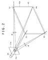
- FIG. 2 is a diagram showing an example of a diffractive optical element.
- FIG. 3 is a diagram showing an example of a liquid crystal display panel.
- FIG. 4 is a diagram showing an example of the form of arrangement of pixels and microlenses.
- FIG. 5 is a diagram showing a concrete example of the liquid crystal display panel.
- FIG. 6 is a diagram showing a second example of a single-panel type liquid crystal projector.
- FIG. 7 shows diagrams illustrating an example of a refraction type optical element.
- FIG. 8 is a diagram showing an example of a light source unit.
- FIG. 9 is a diagram showing an example of a light source unit.
- FIG. 10 is a diagram showing an example of each laser.
- FIG. 11 shows diagrams illustrating an example of each laser.
- FIG. 12 is a diagram showing an example of a pixel arrangement.
- FIG. 13 is a diagram showing an example in which each laser is integrated in one substrate.
- FIG. 14 is a diagram showing an example of a two-panel type liquid crystal projector.
- FIG. 15 is a diagram showing an example of a liquid crystal display panel.
- FIG. 16 is a diagram showing an example of a two-panel type liquid crystal projector.
- FIG. 17 is a diagram showing an example of a three-panel type liquid crystal projector.
- FIG. 18 is a diagram showing a portable telephone terminal as an example of an image reproducing device according to the present invention.
- a case of a single-panel system using one liquid crystal display panel (liquid crystal light valve) for three colors of red, green, and blue will be shown as a first embodiment.
- FIGS. 1 to 5 (Case of Using Diffractive Optical Element): FIGS. 1 to 5
- FIG. 1 illustrates a case of using a diffractive optical element as a light beam diffusing and shaping optical element, as a first example of basic configuration of a single-panel type liquid crystal projector.
- an X-direction, a Y-direction, and a Z-direction are defined as shown in the figures.
- the Y-direction is a direction perpendicular to a paper plane in FIG. 1 .
- a red laser 11 R As a light source, a red laser 11 R, a green laser 11 G, and a blue laser 11 B are arranged and disposed in the X-direction.
- a semiconductor laser is used as each of the red laser 11 R and the blue laser 11 B.
- an InAlGaP base laser or the like is used as the red laser 11 R.
- a GaN base or InGaN base laser is used as the blue laser 11 B.
- a semiconductor laser emitting green laser light is not realized at present.
- a solid-state laser pumped by a semiconductor laser that is, a so-called DPSS (Diode Pumped Solid State) laser, for example YVO 4 +KTP(KTiOPO 4 ), crystal PPLN (Periodically Poled LiNbO 3 ), PP (Periodically Poled) MgO.LN(LiNbO 3 ) or the like is used.
- the oscillation mode of the red laser 11 R, the green laser 11 G, and the blue laser 11 B may be a multi-mode.
- a narrow stripe width may be achieved in a semiconductor laser, and periodical polarization inversion (periodically poled) may be achieved in a solid-state laser.
- a multi-mode semiconductor laser or solid-state laser can be used as the red laser 11 R, the green laser 11 G, and the blue laser 11 B.
- a single mode semiconductor laser or solid-state laser may be used.
- being able to use up to multi-mode oscillation rather than mode control improves a yield of usable semiconductor lasers and reduces manufacturing cost.
- a red, a green, and a blue laser light beams 1 R, 1 G, and 1 B emitted from the red laser 11 R, the green laser 11 G, and the blue laser 11 B are for example respectively passed through ⁇ /2 plates (1 ⁇ 2-wavelength plates) 29 R, 29 G, and 29 B, and made incident on a diffractive optical element 21 .
- Laser light emitted from semiconductor lasers or solid-state lasers does not necessarily have a constant direction of polarization between the devices because of variations in internal electric field of the lasers.
- the direction of polarization is also varied depending on accuracy in assembly of the devices.
- the direction of polarization of laser light beams 3 R, 3 G, and 3 B of respective colors incident on a liquid crystal display panel 40 to be described later can be made to coincide with the axis of polarization of the liquid crystal display panel 40 .
- the direction of polarization may be corrected by using an appropriate phase difference film or retardation plate in place of the ⁇ /2 plates.
- solid-state lasers pumped by a generally used Al;GaAs base semiconductor laser and using a YVO 4 +KTP second harmonic are changed in direction of polarization from device to device, and many of the solid-state lasers have a polarization ratio of about 10.
- the polarization ratio can be increased by compensating for and optimizing a retardation value using an appropriate phase difference film.
- a diffraction type or refraction type light beam diffusing and shaping optical element diffuses and shapes a laser light beam emitted from a semiconductor laser or a solid-state laser as a light source of the projector over an entire display area of the liquid crystal display panel as a liquid crystal light valve.
- the example of FIG. 1 is a case of using a diffractive optical element as the light beam diffusing and shaping optical element.
- the diffractive optical element (DOE) itself is known as a “diffuser”, a “beam shaper” or the like.
- Reference Document 1 (Adam Fedor; Digital Optics Corp. “Binary Optic Diffuser Design”) shows the diffusion and shaping of a light beam by a “diffuser” or a “beam shaper”.
- Reference Document 2 (Yoshifumi Ikeda “Diffraction Type Lens”; OPTRONICS, 2005, No. 3, pp. 175-178) shows a method of manufacturing a “diffraction type lens” or the like.
- a diffuser diffracts light at each point of an incident light beam to each point on an output plane such that light at a certain point of the incident light beam is diffracted to a large number of points on the output plane (1:N mapping).
- a beam shaper diffracts light at each point of an incident light beam to each point on an output plane such that light at a certain point of the incident light beam is diffracted to a certain point on the output plane (1:1 mapping).
- a transmission type diffractive optical element 21 R for red, a transmission type diffractive optical element 21 G for green, and a transmission type diffractive optical element 21 B for blue are provided so as to be arranged in a direction of arrangement of the red laser 11 R, the green laser 11 G, and the blue laser 11 B.
- the diffractive optical element 21 R for red diffuses and shapes the red laser light beam 1 R emitted from the red laser 11 R such that the laser light beam is spread over the entire display area of the liquid crystal display panel 40 as shown by laser light beams 2 R and 3 R, and is incident on red pixels of a liquid crystal layer 48 of the liquid crystal display panel 40 , as will be described later.
- the diffractive optical element 21 G for green diffuses and shapes the green laser light beam 1 G emitted from the green laser 11 G such that the laser light beam is spread over the entire display area of the liquid crystal display panel 40 as shown by laser light beams 2 G and 3 G, and is incident on green pixels of the liquid crystal layer 48 .
- the diffractive optical element 21 B for blue diffuses and shapes the blue laser light beam 1 B emitted from the blue laser 11 B such that the laser light beam is spread over the entire display area of the liquid crystal display panel 40 as shown by laser light beams 2 B and 3 B, and is incident on blue pixels of the liquid crystal layer 48 .
- the diffractive optical element 21 R for red, the diffractive optical element 21 G for green, and the diffractive optical element 21 B for blue are each a Diffuser, as shown in FIG. 2 (in FIG. 2 , however, the refraction of light by a field lens 31 shown in FIG. 1 is omitted)
- a diffractive optical element 21 a for a certain color diffracts a laser light beam 1 a incident on a diffraction pattern forming part 21 c thereof to an entire display area 40 a of the liquid crystal display panel 40 including points P 1 , P 2 , P 3 , and P 4 at respective corners by mapping as described above.
- the diffractive optical element 21 as a whole is configured such that pieces of diffracted light of the respective colors from the diffractive optical elements 21 R, 21 G, and 21 B are each diffused in the form of dots and uniformized such that dots are superimposed on each other on the display area 40 a , whereby the display area 40 a is irradiated.
- an angle ⁇ of divergence of the light is determined by the beam diameter of the laser light beam 1 a , and this angle ⁇ of divergence of the light can be made sufficiently small, such as one degree or less, as will be described later.
- a laser light beam emitted from a laser generally has a Gaussian shape. It is difficult to uniformly irradiate the liquid crystal display panel 40 with the laser light beam as it is. However, by thus diffusing and shaping the laser light beam by the diffractive optical element 21 and then irradiating the liquid crystal display panel 40 with the laser light beam, a uniform luminance distribution can be obtained on the liquid crystal display panel 40 .
- the diffractive optical elements 21 R, 21 G, and 21 B for the respective colors are desirably formed in a state of being integrated on one transparent substrate. This makes it possible to align the diffractive optical elements 21 R, 21 G, and 21 B easily and accurately, and miniaturize the diffractive optical element 21 as a whole, as compared with a case where the diffractive optical elements 21 R, 21 G, and 21 B are aligned and disposed after being formed individually.
- the diffractive optical element 21 as described above can be created after a computer simulation is performed on the basis of the beam diameter and the beam shape of the laser light beams 1 R, 1 G, and 1 B of the respective colors, a luminance distribution on a screen to be obtained, and the like.
- a field lens 31 is disposed in front of the diffractive optical element 21 , the field lens 31 converting the red laser light beam 2 R diffused and shaped by the diffractive optical element 21 R for red, the green laser light beam 2 G diffused and shaped by the diffractive optical element 21 G for green, and the blue laser light beam 2 B diffused and shaped by the diffractive optical element 21 B for blue into respective laser light beams 3 R, 3 G, and 3 B of substantially collimated light, and then making the laser light beams 3 R, 3 G, and 3 B incident on the liquid crystal display panel 40 .
- the liquid crystal display panel 40 is a transmissive type liquid crystal display device having a liquid crystal layer 48 formed between an incidence side substrate 41 and an emission side substrate 46 .
- Polarizing plates 33 and 34 are disposed on the rear side and the front side of the liquid crystal display panel 40 .
- a microlens array is formed in the incidence side substrate 41 of the liquid crystal display panel 40 .
- a microlens array 44 made of a transparent resin or the like is formed between transparent substrates 42 and 43 made of quartz or the like, and that a counter common electrode 45 made of a transparent conductive material such as ITO (Indium Tin Oxide) or the like is formed on the transparent substrate 43 .
- ITO Indium Tin Oxide
- a scanning line made of polysilicon, a signal line made of aluminum or the like, a pixel electrode made of a transparent conductive material such as ITO or the like, and a TFT (Thin Film Transistor) as a pixel switching element are formed as a liquid crystal driving circuit 47 of an active matrix system on one surface side of the transparent substrate made of quartz or the like.
- the counter common electrode 45 and the liquid crystal driving circuit 47 are disposed in a state of being opposed to each other such that a small gap is formed between the incidence side substrate 41 and the emission side substrate 46 described above.
- a liquid crystal is injected between the counter common electrode 45 and the liquid crystal driving circuit 47 to form the liquid crystal layer 48 .
- a red pixel (sub-pixel for red display) Pr, a green pixel (sub-pixel for green display) Pg, and a blue pixel (sub-pixel for blue display) Pb are formed.
- the above-described liquid crystal driving circuit 47 is formed such that a large number of sets (display units) of a red pixel Pr, a green pixel Pg, and a blue pixel Pb are formed in a so-called A arrangement as viewed from the incidence side of the laser light beams, and that the microlens array 44 has a large number of hexagonal microlenses 44 a formed at a ratio of one microlens to one display unit as viewed from the incidence side of the laser light beams.
- Reference 19 a denotes a light shielding layer (black layer) and a scanning line.
- Reference number 19 c denotes a signal line.
- display units can be arranged in a square array.
- the microlenses 44 a are in a rectangular (square or oblong) form as viewed from the incidence side of the laser light beams.
- the square array is suitable for display of text and the like, and is often used in a computer display of VGA, SXGA or the like.
- each of the microlenses 44 a is desirably aspheric in order to suppress spherical aberration.
- the diffractive optical element 21 R for red diffuses and shapes the red laser light beam 1 R emitted from the red laser 11 R so that the red laser light beam 1 R ultimately enters the red pixels Pr of the liquid crystal layer 48 via the microlenses 44 a .
- the diffractive optical element 21 G for green diffuses and shapes the green laser light beam 1 G emitted from the green laser 11 G so that the green laser light beam 1 G ultimately enters the green pixels Pg of the liquid crystal layer 48 via the microlenses 44 a .
- the diffractive optical element 21 B for blue diffuses and shapes the blue laser light beam 1 B emitted from the blue laser 11 B so that the blue laser light beam 1 B ultimately enters the blue pixels Pb of the liquid crystal layer 48 via the microlenses 44 a.
- Each of the lasers 11 R, 11 G, and 11 B is considered to be a pseudo point source of light.
- the angle ⁇ of divergence of the light shown in FIG. 1 and FIG. 2 can be made sufficiently small, an amount of light applied onto the screen can be increased significantly as compared with a case of using a lamp as a light source, and light use efficiency can be improved to about 30% even with the single-panel system. It is thus possible to reduce laser output and suppress heat generation in each laser. Such a highly efficient liquid crystal projector has never existed thus far.
- a red image signal is applied to parts of the pixels Pr of the liquid crystal layer 48 of the liquid crystal display panel 40 so that transmittance of the parts of the pixels Pr is modulation-controlled.
- a green image signal is applied to parts of the pixels Pg of the liquid crystal layer 48 so that transmittance of the parts of the pixels Pg is modulation-controlled.
- a blue image signal is applied to parts of the pixels Pb of the liquid crystal layer 48 so that transmittance of the parts of the pixels Pb is modulation-controlled.
- red image light is obtained as laser light passed through the parts of the pixels Pr
- green image light is obtained as laser light passed through the parts of the pixels Pg
- blue image light is obtained as laser light passed through the parts of the pixels Pb.
- Multi-color image light resulting from synthesizing these pieces of image light of the respective colors is obtained as laser light passed through the liquid crystal display panel 40 .
- a projection lens 50 projects this multi-color image light onto the screen outside the projector.
- the projection lens 50 is formed by combining a plurality of lenses.
- a constitution is formed as follows.
- An InAlGaP base semiconductor laser having an oscillation wavelength of 635 nm to 640 nm is used as the red laser 11 R.
- a GaN base semiconductor laser having an oscillation wavelength of 445 nm is used as the blue laser 11 B.
- Each has an output of 100 mW, has a light divergence angle of 30 degrees (FWHM) in a vertical direction, has a light divergence angle of 10 degrees in a horizontal direction, has a single mode as a transverse mode, and has a multi-mode as a longitudinal mode.
- An output is 100 mW, a transverse mode is a single mode, and a longitudinal mode is a multi-mode.
- Parallelism between the laser light beams 1 R, 1 G, and 1 B is important in controlling angles of incidence on the field lens 31 of the laser light beams 2 R, 2 G, and 2 B, which are diffused and shaped by the diffractive optical element 21 .
- the parallelism is set to fall within one degree in the X-direction and the Y-direction. Specifically, control is performed so as to achieve such parallelism while oscillating the laser light by a so-called active alignment system.
- a distance between the laser light beams 1 R and 1 G and a distance between the laser light beams 1 G and 1 B are each set to about 1.5 mm.
- the beam size (beam diameter) of the laser light beams 1 R, 1 G, and 1 B on the diffractive optical element 21 is set to about 0.6 mm to 0.8 mm.
- the microlenses 44 a are formed by a transparent resin (an epoxy base, a thiourethane base or the like) having a refractive index of 1.669.
- the width Ds of a signal line 19 c is 2.0 ⁇ m.
- the width Dp of pixels Pr, Pg, and Pb is 8.7 ⁇ m.
- the pitch of a display unit formed of one pixel Pr, one pixel Pg, and one pixel Pb is 32.1 ⁇ m.
- the liquid crystal display panel 40 for example, 188 display units thus having a pitch of 32.1 ⁇ m in the X-direction and having a pitch of 20.4 ⁇ m in the Y-direction are formed in the X-direction, and 220 sets (440 columns) of display units are formed in the Y-direction with two columns as one set.
- the entire display area is slightly more than 6 mm in the X-direction and is slightly less than 9 mm in the Y-direction. A higher definition is possible.
- the microlenses 44 a have a radius of curvature of 25.2 ⁇ m, an aspheric surface constant of ⁇ 0.765, a focal length fa of about 120 ⁇ m from a principal point H as a converted value in the air.
- the single-panel type liquid crystal projector in the example of FIG. 1 described above uses the red laser 11 R, the green laser 11 G, and the blue laser 11 B each formed by a semiconductor laser or a solid-state laser as a light source, and uses the diffractive optical elements 21 R, 21 G, and 21 B for the respective colors. Therefore the light source unit and the optical system of the projector as a whole can be greatly miniaturized.
- the maximum angle of diffraction of the diffractive optical elements 21 R, 21 G, and 21 B is in a trade-off relation to uniformity of luminance on the liquid crystal display panel 40 .
- the maximum angle of diffraction of the diffractive optical elements 21 R, 21 G, and 21 B can be increased to about 30 degrees without impairing uniformity of luminance. It is thereby possible to shorten a distance between the diffractive optical element 21 and the liquid crystal display panel 40 , and shorten the length of the projector as a whole.
- the optical system of the projector as a whole can be miniaturized to a width of 1 cm in the X-direction and the Y-direction, a length of 3.5 cm in the Z-direction, and a volume of a few cm 3 .
- the laser light source formed of the red laser 11 R, the green laser 11 G, and the blue laser 11 B is used as a light source, the light divergence angle ⁇ can be sufficiently decreased to for example one degree or less, and the light use efficiency can be sufficiently increased to for example about 30%. Hence, laser output power can be reduced, which is advantageous in terms of a measure against generation of heat and a measure for safety.
- the light divergence angle is large (normally about 10 to 15 degrees) without an aperture or the like being used, and in the case of a single-panel system, a color mixture occurs and color purity is lowered.
- the light divergence angle ⁇ can be sufficiently decreased to for example one degree or less, and therefore a decrease in color purity due to a color mixture does not occur.
- the angle of incidence of the light on the projection lens 50 can also be decreased, a lens having a large F-number can be used as the projection lens 50 , so that freedom of design of the projection lens 50 is increased, and the cost of the projection lens 50 can be reduced.
- black display can be achieved by making corresponding display units of the liquid crystal layer 48 block light by the liquid crystal driving circuit 47 rather than turning off the laser light beams 1 R, 1 G, and 1 B of the respective colors. Therefore image contrast is not decreased.
- the light divergence angle ⁇ and the angle ⁇ of incidence can be decreased as described above, a decrease in contrast due to an oblique incidence of light on the polarizing plates 33 and 34 can be reduced.
- FIG. 6 illustrates a case of using a refraction type optical element as a light beam diffusing and shaping optical element, as a second example of basic configuration of a single-panel type liquid crystal projector.
- a red laser 11 R, a green laser 11 G, and a blue laser 11 B are provided as a light source.
- the lasers 11 R, 11 G, and 11 B are arranged such that for example laser light beams 1 R and 1 B on both sides are inclined at predetermined angles, respectively, with respect to a laser light beam 1 G at a center so as to be directed to the principal point of a field lens 31 .
- the design of an optical system is easy when center light is made incident obliquely and the center lines of emitted light are made to coincide with each other.
- the laser light beams 1 R, 1 G, and 1 B of the respective colors may be parallel to each other as in the example of FIG. 1 .
- the laser light beams 1 R, 1 G, and 1 B of the respective colors emitted from the respective lasers 11 R, 11 G, and 11 B are for example passed through ⁇ /2 plates 29 R, 29 G, and 29 B, respectively, and made incident on a refraction type optical element 23 .
- the refraction type optical element itself is known, and reference can be made on the Internet (URL; http://www.rpcphotonics.com/engineer_diffuser.htm, for example) and the like.
- the refraction type optical element is formed by two-dimensionally assembling microlenses having various shapes and curvatures.
- the refraction type optical element is able to diffuse and shape a light beam by refraction of the light.
- Each microlens has a different curvature and a different radius, the length of a side being about 50 ⁇ m.
- Light that has entered each microlens is refracted by the microlens, superposed, and ultimately shaped into a predetermined form.
- the distribution of luminance can also be uniformized.
- the laser light beams 1 R, 1 G, and 1 B of the respective colors are diffused and shaped so as to be spread over the entire display area of a liquid crystal display panel 40 as shown by laser light beams 2 R, 2 G, and 2 B, and be incident on corresponding pixels of a liquid crystal layer 48 of the liquid crystal display panel 40 .
- light 9 in FIG. 7(B) represents a state of refraction of light entering a certain microlens.
- the refractive index of the refraction type optical element is determined by only dispersion relation of a material forming the element, and the refractive index for light of respective colors is almost unchanged in a visible light region. Therefore the refraction type optical element 23 can be thus made common to the laser light beams 1 R, 1 G, and 1 B of the respective colors.
- a field lens 31 is disposed between the refraction type optical element 23 and the liquid crystal display panel 40 to convert the laser light beams 2 R, 2 G, and 2 B diffused and shaped by the refraction type optical element 23 into respective laser light beams of substantially collimated light and make the laser light beams incident on the liquid crystal display panel 40 .
- the configuration of the liquid crystal display panel 40 is the same as in the example of FIG. 1 , including a respect in which a microlens array 44 is formed in an incidence side substrate 41 as shown in FIG. 3 .
- the lasers 11 R, 11 G, and 11 B of the light source unit are simply arranged in one direction as in FIG. 1 or FIG. 6 , and the laser light beams 1 R, 1 G, and 1 B emitted from the respective lasers 11 R, 11 G, and 11 B are made incident on the diffractive optical element 21 or the refraction type optical element 23 as they are, a difference between adjacent laser light beams may not be sufficiently small because of the packages of the lasers or the like.
- a light source unit 10 is formed as shown in FIG. 8 .
- a central green laser 11 G formed by a DPSS laser is placed in a recessed position with respect to a red laser 11 R and a blue laser 11 B.
- One end of a polarization mode optical fiber 13 G is connected to the green laser 11 G.
- Another end of the optical fiber 13 G is guided between a can package 11 r of the red laser 11 R and a can package 11 b of the blue laser 11 B.
- a green laser light beam 1 G is emitted from the other end of the optical fiber 13 G.
- a distance between a laser light beam 1 R and the laser light beam 1 G and between a laser light beam 1 B and the laser light beam 1 G can be shortened, and in the example of FIG. 1 , an interval (pitch) between the diffractive optical elements 21 R and 21 G and the diffractive optical elements 21 B and 21 G can be shortened.
- the green laser 11 G can be placed at a distance from the red laser 11 R and the blue laser 11 B. Therefore a degree of freedom can be given to the disposition of the light source within a small electronic device, in particular.
- Such a configuration is convenient because the green laser 11 G formed by a DPSS laser is generally larger than the red laser 11 R and the blue laser 11 B formed by a semiconductor laser.
- a laser light beam emitted from a semiconductor laser does not have a circular sectional shape but diverges at different angles in a vertical direction and a horizontal direction as described above, a laser light beam entering the diffractive optical element 21 or the refraction type optical element 23 desirably has a sectional shape close to a circular shape.
- a laser light beam emitted from a DPSS laser has a rather small diameter in practice.
- the light divergence angle ⁇ shown in FIG. 1 , FIG. 2 , and FIG. 6 is in accordance with the beam diameter of the laser light beam emitted from the laser: the smaller the beam diameter, the smaller the light divergence angle ⁇ .
- the diffractive optical element 21 R for red, the diffractive optical element 21 G for green, and the diffractive optical element 21 B for blue are each formed as a so-called Diffuser that uniformly diffuses diffracted light in a two-dimensional direction by a periodic pitch
- a laser light beam needs to be incident on the diffractive optical element 21 R for red, the diffractive optical element 21 G for green, and the diffractive optical element 21 B for blue in such a manner as to be spread over a plurality of fundamental periods.
- the beam diameter of the laser light beam 1 G incident on the diffractive optical element 21 G is too small, the green diffracted light cannot be uniformly diffused in the two-dimensional direction.
- the laser light beams 1 R, 1 G, and 1 B of the respective colors incident on the diffractive optical element 21 desirably have a beam diameter of about 0.5 mm to 1.0 mm.
- a light source unit is formed as shown in FIG. 9 .
- a laser light beam 1 Go emitted from a central green laser 11 G formed by a DPSS laser is increased in beam diameter by a beam expander 12 G, and then made incident on a diffractive optical element 21 .
- the sectional shape of a laser light beam 1 Ro emitted from a red laser 11 R is made to approximate a circular shape by a collimation unit 14 R including two cylindrical lenses 15 R and 16 R. Further, the laser light beam 1 Ro is reflected twice by a prism 17 R to become a laser light beam 1 R passing a position near the laser light beam 1 G.
- the sectional shape of a laser light beam 1 Bo emitted from a blue laser 11 B (can package 11 b ) is made to approximate a circular shape by a collimation unit 14 B including two cylindrical lenses 15 B and 16 B. Further, the laser light beam 1 Bo is reflected twice by a prism 17 B to become a laser light beam 1 B passing a position near the laser light beam 1 G.
- the red laser light beam 1 R and the blue laser light beam 1 B can have a beam diameter of 0.8 mm ⁇ and a section close to a circular shape, the astigmatism of the red laser light beam 1 R and the blue laser light beam 1 B can be reduced, and the laser light beam 1 G can have a beam diameter of 0.6 mm ⁇ at a position on the diffractive optical element 21 .
- an interval between the laser light beams 1 R and 1 G and an interval between the laser light beams 1 B and 1 G can each be made sufficiently small, such as 1.5 mm or the like.
- the respective emission surfaces (output surfaces) of a red laser 11 R, a green laser 11 G, and a blue laser 11 B can be extended or arranged in one direction. This is important in order to increase an amount of emitted light, in particular.
- FIG. 10 shows an example thereof.
- FIG. 10 is a diagram as viewed from the side of a liquid crystal display panel 40 .
- the green laser 11 G formed by a DPSS laser has a plurality of output surfaces 18 g arranged and formed in the Y-direction on a package 11 g thereof, so that a laser light beam is emitted from each of the output surfaces 18 g
- the red laser 11 R and the blue laser 11 B each have a plurality of semiconductor lasers 18 a arranged and formed in the Y-direction on a heat sink 18 h , so that a laser light beam is emitted from each of the semiconductor lasers 18 a.
- each of the red laser 11 R and the blue laser 11 B has a metallic block 18 c of copper or the like formed on one surface of a Peltier element 18 p and has a plurality of semiconductor lasers 18 a arranged and formed in the Y-direction on one surface of the metallic block 18 c , so that a laser light beam 1 a is emitted from each of the semiconductor lasers 18 a .
- a laser light beam is emitted from each semiconductor laser 18 s as an edge emitting multi stripe semiconductor laser.
- the liquid crystal display panel 40 may have a so-called square array in which pixels of a same color are arranged in the Y-direction, as shown in FIG. 12 ( FIG. 12 is a diagram as viewed from the incidence side of the laser light beams).
- the square array is desirable especially when text or graphics are displayed.
- the microlenses 44 a shown in FIG. 3 can be cylindrical lenses extending in the Y-direction. Also when the microlenses 44 a are cylindrical lenses, the sections thereof on a light incidence side desirably have an elliptic shape, a hyperbolic shape or the like.
- a collimator lens is used in place of the above-described field lens 31 .
- the light amount of total laser light of each color can be uniformized or adjusted.
- a red laser 11 R, a green laser 11 G, and a blue laser 11 B can be integrated in one substrate.
- FIG. 13 shows an example thereof.
- a heat sink laser array 19 in which a plurality of lasers (emitting surfaces) 19 r emitting red laser light, a plurality of lasers (emitting surfaces) 19 g emitting green laser light, and a plurality of lasers (emitting surfaces) 19 b emitting blue laser light are arranged and formed in the Y-direction is used as a laser light source having the red laser 11 R, the green laser 11 G, and the blue laser 11 B integrated therein.
- the red laser light emitted from the lasers 19 r , the green laser light emitted from the lasers 19 g , and the blue laser light emitted from the lasers 19 b are each diffused and shaped by a diffractive optical element 21 (or a refraction type optical element 23 ), and made incident on a red pixel Pr, a green pixel Pg, and a blue pixel Pb of a liquid crystal layer 48 via a collimator lens 32 and via the microlenses 44 a of a liquid crystal display panel 40 .
- the liquid crystal display panel 40 can have a square array as shown in FIG. 12 .
- the microlenses 44 a can be cylindrical lenses extending in the Y-direction.
- a laser light beam of any color may be arbitrarily positioned at a center.
- a Diffuser is used as the diffractive optical element 21 , in order to increase the above-described angle of diffraction, it is desirable to position a blue laser light beam of a short wavelength at a center unlike each of the examples shown in the figures.
- a case of a two-panel system using two liquid crystal display panels (liquid crystal light valves) for three colors of red, green, and blue will be shown as a second embodiment.
- FIG. 14 and FIG. 15 are identical to FIG. 14 and FIG. 15
- FIG. 14 shows an example of a two-panel type liquid crystal projector.
- a red laser 11 R and a blue laser 11 B are disposed in proximity to each other, and a green laser 11 G is disposed at a different position.
- the red laser 11 R and the blue laser 11 B are each a semiconductor laser as described above.
- the green laser 11 G is a DPSS laser as described above.
- a collimation optical system for bringing the sectional shape of a laser light beam emitted from each of the red laser 11 R and the blue laser 11 B close to a circular shape be provided for the red laser 11 R and the blue laser 11 B, and a beam expander for increasing the beam diameter of a laser light beam emitted from the green laser 11 G be provided for the green laser 11 G.
- a diffractive optical element 21 R for red and a diffractive optical element 21 B for blue are arranged in front of the red laser 11 R and the blue laser 11 B.
- the red laser light beam 1 R emitted from the red laser 11 R and the blue laser light beam 1 B emitted from the blue laser 11 B are each diffused and shaped so as to be spread over the entire display area of a liquid crystal display panel 80 to be described later and be incident on corresponding pixels thereof.
- the laser light beams 2 R and 2 B diffused and shaped by the diffractive optical element 21 R for red and the diffractive optical element 21 B for blue are converted into laser light beams 3 R and 3 B, respectively, as collimated light beams by a field lens 31 RB, and then made incident on the liquid crystal display panel 80 .
- liquid crystal display panel 80 a liquid crystal layer constituting red and blue pixels is formed between an incidence side substrate, in which a microlens array is formed, and an emission side substrate.
- an incidence side substrate 81 has a microlens array 84 formed between transparent substrates 82 and 83 , and that a counter common electrode 85 made of a transparent conductive material such as ITO or the like is formed on the transparent substrate 83 .
- a scanning line, a signal line, a pixel electrode made of a transparent conductive material such as ITO or the like, and a TFT as a pixel switching element are formed as a liquid crystal driving circuit 87 of an active matrix system on one surface side of the transparent substrate.
- the counter common electrode 85 and the liquid crystal driving circuit 87 are disposed in a state of being opposed to each other such that a small gap is formed between the incidence side substrate 81 and the emission side substrate 86 described above.
- a liquid crystal is injected between the counter common electrode 85 and the liquid crystal driving circuit 87 to form a liquid crystal layer 88 .
- a red pixel Pr and a blue pixel Pb are formed.
- Microlenses 84 a are formed at a ratio of one microlens to one set (display unit) of a red pixel Pr and a blue pixel Pb. In addition, when pixels of a same color are arranged in a direction perpendicular to the paper plane of FIG. 15 , the microlenses 84 a can be cylindrical lenses extending in the direction perpendicular to the paper plane of FIG. 15 .
- respective pieces of partial laser light 3 r and 3 b of the red and blue laser light beams 3 R and 3 B converted into the collimated light beams by the field lens 31 RB and then made incident on the liquid crystal display panel 80 are each distributed and condensed by the microlenses 84 a , and enter the corresponding pixels Pr and Pb of the liquid crystal layer 88 .
- a red image signal is applied to the part of the pixel Pr of the liquid crystal layer 88 of the liquid crystal display panel 80 so that transmittance of the part of the pixel Pr is modulation-controlled.
- a blue image signal is applied to the part of the pixel Pb of the liquid crystal layer 88 so that transmittance of the part of the pixel Pb is modulation-controlled.
- red image light is obtained as laser light passed through the part of the pixel Pr
- blue image light is obtained as laser light passed through the part of the pixel Pb.
- the red image light 5 R and the blue image light 5 B are passed through a dichroic prism 63 , and then made incident on a projection lens 50 .
- a diffractive optical element 21 G for green is arranged in front of the green laser 11 G.
- the green laser light beam 1 G emitted from the green laser 11 G is diffused and shaped so as to be spread over the entire display area of a liquid crystal display panel 65 G to be described later and be incident on each pixel thereof.
- the laser light beam 2 G diffused and shaped by the diffractive optical element 21 G for green is reflected by a mirror 37 , converted into a laser light beam 3 G as a collimated light beam by a field lens 31 G, and then made incident on the liquid crystal display panel 65 G.
- the liquid crystal display panel 65 G is a liquid crystal display device for single color display.
- a pixel thereof corresponds to a display unit formed of a red pixel Pr and a blue pixel Pb of the above-described liquid crystal display panel 80 .
- a green image signal is applied to the part of each pixel thereof so that transmittance of the part of each pixel is modulation-controlled.
- green image light 5 G is obtained as laser light passed through the liquid crystal display panel 65 G.
- the green image light 5 G is reflected by a reflection coating 63 a of the dichroic prism 63 , and then made incident on the projection lens 50 .
- multi-color image light can be projected onto a screen outside the projector.
- an angle between the red laser light beam 1 R and the blue laser light beam 1 B is set at six degrees.
- the diffractive optical element 21 G for green is a transmission type diffractive optical element.
- a reflection type diffractive optical element may be disposed as a diffractive optical element for green at the position of the mirror 37 .
- a refraction type optical element as described above can be used in place of each of the diffractive optical elements.
- Red light having a wavelength of about 620 nm has a highest degree of recognition as red.
- current semiconductor lasers providing laser light having a wavelength of about 620 nm lack stability with respect to temperature, for example, and are thus inferior in reliability.
- a semiconductor laser providing laser light having a wavelength of about 640 nm, which laser light has a somewhat lower degree of recognition as red but is of high reliability, is used as a red laser.
- two red lasers are used to increase the degree of recognition as red.
- a red laser 11 Rs and a green laser 11 G are disposed in proximity to each other at the position of the green laser 11 G in the example of FIG. 14 .
- the red laser 11 Rs is a semiconductor laser similar to the red laser 11 R.
- a reflection type diffractive optical element 21 Rs for red and a reflection type diffractive optical element 21 Ga for green are arranged in front of the red laser 11 Rs and the green laser 11 G, respectively.
- a red laser light beam 1 Rs emitted from the red laser 11 Rs and a green laser light beam 1 G emitted from the green laser 11 G are each reflected, and then diffused and shaped so as to be spread over the entire display area of a liquid crystal display panel 90 to be described later and be incident on corresponding pixels thereof.
- the laser light beams 2 Rs and 2 G reflected and then diffused and shaped by the diffractive optical element 21 Rs for red and the diffractive optical element 21 Ga for green are converted into laser light beams 3 Rs and 3 G, respectively, as collimated light beams by a field lens 31 RG, and then made incident on the liquid crystal display panel 90 .
- liquid crystal display panel 90 a liquid crystal layer constituting red and blue pixels is formed between an incidence side substrate, in which a microlens array is formed, and an emission side substrate.
- the liquid crystal display panel 90 is obtained by replacing the blue pixels Pb of the liquid crystal display panel 80 shown in FIG. 15 with green pixels.
- red image light 5 Rs and green image light 5 G are obtained as laser light passed through the liquid crystal display panel 90 .
- An optical system for a red laser 11 R and a blue laser 11 B at a different position is the same as in the example of FIG. 14 .
- the red image light 5 Rs passed through the liquid crystal display panel is reflected by a reflection coating 63 a of a dichroic prism 63 , combined with red image light 5 R passed through a liquid crystal display panel 80 , and then made incident on a projection lens 50
- the green image light 5 G passed through the liquid crystal display panel 90 is reflected by the reflection coating 63 a of the dichroic prism 63 , and then made incident on the projection lens 50 .
- Blue image light 5 B passed through the liquid crystal display panel 80 is passed through the dichroic prism 63 , and then made incident on the projection lens 50 .
- multi-color image light can be projected onto a screen outside the projector, and the degree of recognition as red in the multi-color image can be increased.
- the angle of the laser light beam 1 Rs with respect to the laser light beam 1 G is set at 1.5 degrees, and the angle of the laser light beam 2 Rs with respect to the laser light beam 2 G is set at 3 degrees.
- a refraction type optical element as described above can be used in place of each of the diffractive optical elements.
- a case of a three-panel system using separate liquid crystal display panels (liquid crystal light valves) for three colors of red, green, and blue will be shown as a third embodiment.
- FIG. 17 shows an example of a three-panel type liquid crystal projector.
- a red laser 11 R, a green laser 11 G, and a blue laser 11 B are disposed at different positions.
- a diffractive optical element 21 R for red diffuses and shapes a red laser light beam 1 R emitted from the red laser 11 R such that the red laser light beam 1 R is spread over the entire display area of a liquid crystal display panel 65 R to be described later and is incident on each pixel thereof.
- a diffractive optical element 21 G for green diffuses and shapes a green laser light beam 1 G emitted from the green laser 11 G such that the green laser light beam 1 G is spread over the entire display area of a liquid crystal display panel 65 G to be described later and is incident on each pixel thereof.
- a reflection type diffractive optical element 21 Ba for blue reflects a blue laser light beam 1 B emitted from the blue laser 11 B, and diffuses and shapes the blue laser light beam 1 B such that the blue laser light beam 1 B is spread over the entire display area of a liquid crystal display panel 65 B to be described later and is incident on each pixel thereof.
- the laser light beam 2 R diffused and shaped by the diffractive optical element 21 R for red is reflected by a mirror 39 , converted into a laser light beam 3 R as a collimated light beam by a field lens 31 R, and then made incident on the liquid crystal display panel 65 R.
- the laser light beam 2 G diffused and shaped by the diffractive optical element 21 G for green is converted into a laser light beam 3 G as a collimated light beam by a field lens 31 G, and then made incident on the liquid crystal display panel 65 G.
- the laser light beam 2 B reflected and diffused and shaped by the diffractive optical element 21 Ba for blue is converted into a laser light beam 3 B as a collimated light beam by a field lens 31 B, and then made incident on the liquid crystal display panel 65 B.
- the liquid crystal display panel 65 R is a liquid crystal display device for display of the single color of red.
- the liquid crystal display panel 65 G is a liquid crystal display device for display of the single color of green.
- the liquid crystal display panel 65 B is a liquid crystal display device for display of the single color of blue.
- red image light 5 R is obtained as laser light passed through the liquid crystal display panel 65 R.
- Green image light 5 G is obtained as laser light passed through the liquid crystal display panel 65 G.
- Blue image light 5 B is obtained as laser light passed through the liquid crystal display panel 65 B.
- the green image light 5 G is passed through a cross dichroic prism 69 , and then made incident on a projection lens 50 .
- the red image light 5 R is reflected by a reflection coating 69 r of the cross dichroic prism 69 , and then made incident on the projection lens 50 .
- the blue image light 5 B is reflected by a reflection coating 69 b of the cross dichroic prism 69 , and then made incident on the projection lens 50 .
- multi-color image light can be projected onto a screen outside the projector.
- a reflection type diffractive optical element for red may be disposed at the position of the mirror 39 in place of the transmission type diffractive optical element 21 R for red.
- a mirror may be disposed at the position of the diffractive optical element 21 Ba for blue in place of the reflection type diffractive optical element 21 Ba for blue, and a transmission type diffractive optical element may be disposed at a position in the rear thereof.
- a refraction type optical element as described above can be used in place of each of the diffractive optical elements.
- Each of the foregoing embodiments is a configuration for the three colors of red, green, and blue. However, a configuration for two or one of the three colors can be made.
- the red laser 11 R, the blue laser 11 B, the diffractive optical element 21 R for red, and the diffractive optical element 21 B for blue in the example of FIG. 1 it suffices not to provide the red laser 11 R, the blue laser 11 B, the diffractive optical element 21 R for red, and the diffractive optical element 21 B for blue in the example of FIG. 1 , and to make the liquid crystal display panel 40 a liquid crystal display device for display of the single color of green.
- FIG. 18 shows an example of an image reproducing device according to the present invention.
- a single-panel type liquid crystal projector 110 as in the example of FIG. 1 or FIG. 6 is built in a portable telephone terminal 100 as a liquid crystal projector according to the present invention.
- the portable telephone terminal 100 is of a folding type such that an opening and closing part 101 provided with a display such as a liquid crystal display, an organic EL display or the like and a receiving speaker can be opened and closed with respect to a base part 102 provided with various keys and a transmitting microphone.
- the liquid crystal projector 110 is built in a side part of the base part 102 on an opposite side from a side where an antenna 103 is provided.
- image data obtained by a portable telephone communication network or obtained by taking a subject by a camera built in the portable telephone terminal 100 and recorded on a recording medium such as a semiconductor memory or a hard disk built in the portable telephone terminal 100 , a memory card loaded in the portable telephone terminal 100 , or the like is processed by an image processing unit within the portable telephone terminal 100 , and converted into a red, a green, and a blue image signal, which are applied to a liquid crystal display panel 40 of the liquid crystal projector 110 .
- multi-color image light 7 can be projected onto a screen 200 outside the portable telephone terminal 100 .
- a wall of a room, the top of a desk, a sheet of paper placed on a desk, and the like can be used as the screen 200 .
- the liquid crystal projector according to the present invention can be built in not only a portable telephone terminal but also a device that processes image data recorded on a recording medium (storage device) built therein or loaded therein and reproduces an image, such as a digital camera (digital still camera), a video camera, a mobile computer, a game machine or the like.
- a recording medium storage device
Landscapes
- Physics & Mathematics (AREA)
- General Physics & Mathematics (AREA)
- Engineering & Computer Science (AREA)
- Multimedia (AREA)
- Signal Processing (AREA)
- Optics & Photonics (AREA)
- Projection Apparatus (AREA)
- Liquid Crystal (AREA)
Applications Claiming Priority (3)
| Application Number | Priority Date | Filing Date | Title |
|---|---|---|---|
| JP2006109938A JP4736921B2 (ja) | 2006-04-12 | 2006-04-12 | 液晶プロジェクタおよび画像再生装置 |
| JP2006-109938 | 2006-04-12 | ||
| PCT/JP2007/057889 WO2007123024A1 (fr) | 2006-04-12 | 2007-04-10 | projecteur à cristaux liquides et dispositif de reproduction d'image |
Publications (2)
| Publication Number | Publication Date |
|---|---|
| US20090161033A1 US20090161033A1 (en) | 2009-06-25 |
| US8334937B2 true US8334937B2 (en) | 2012-12-18 |
Family
ID=38624930
Family Applications (1)
| Application Number | Title | Priority Date | Filing Date |
|---|---|---|---|
| US12/295,911 Expired - Fee Related US8334937B2 (en) | 2006-04-12 | 2007-04-10 | Liquid crystal projector and image reproducing device |
Country Status (7)
| Country | Link |
|---|---|
| US (1) | US8334937B2 (fr) |
| EP (1) | EP2006735A4 (fr) |
| JP (1) | JP4736921B2 (fr) |
| KR (1) | KR20080111048A (fr) |
| CN (1) | CN101421669B (fr) |
| TW (1) | TW200807134A (fr) |
| WO (1) | WO2007123024A1 (fr) |
Cited By (4)
| Publication number | Priority date | Publication date | Assignee | Title |
|---|---|---|---|---|
| US20120075539A1 (en) * | 2009-06-12 | 2012-03-29 | Asahi Glass Company, Limited | Projection display device |
| US20140340652A1 (en) * | 2013-05-17 | 2014-11-20 | Seiko Epson Corporation | Light source device and projector |
| US20150293271A1 (en) * | 2012-12-28 | 2015-10-15 | Asahi Glass Company, Limited | Optical device, projector, and method of producing optical device |
| US10928643B2 (en) * | 2017-03-23 | 2021-02-23 | Nec Display Solutions, Ltd. | Light source device including laser light sources, projector, and speckle reduction method for forming light by mixing diffused lights emitted from laser light source groups |
Families Citing this family (39)
| Publication number | Priority date | Publication date | Assignee | Title |
|---|---|---|---|---|
| US8684532B2 (en) * | 2007-09-19 | 2014-04-01 | Texas Instruments Incorporated | System and method for generating multicolor scan lines and multicolor projection video display incorporating the same |
| JP5157374B2 (ja) * | 2007-11-08 | 2013-03-06 | ソニー株式会社 | 液晶表示素子および投射型液晶表示装置、並びに電子機器 |
| US20090147159A1 (en) * | 2007-12-06 | 2009-06-11 | Young Optics Inc. | Projector |
| JP5262849B2 (ja) * | 2009-03-06 | 2013-08-14 | セイコーエプソン株式会社 | プロジェクター |
| JP5262850B2 (ja) * | 2009-03-06 | 2013-08-14 | セイコーエプソン株式会社 | プロジェクター |
| WO2011025724A1 (fr) * | 2009-08-27 | 2011-03-03 | Dolby Laboratories Licensing Corporation | Système de mélange et de mise en forme optique pour rétroéclairages de dispositif d'affichage et dispositifs d'affichage le comprenant |
| JP2011128205A (ja) | 2009-12-15 | 2011-06-30 | Seiko Epson Corp | 画像表示装置 |
| JP5866968B2 (ja) * | 2011-01-13 | 2016-02-24 | セイコーエプソン株式会社 | プロジェクター |
| EP3364651B1 (fr) | 2011-04-19 | 2020-03-04 | Dolby Laboratories Licensing Corporation | Affichages de projection de luminance élevée et procédés associés |
| JP5845684B2 (ja) * | 2011-07-25 | 2016-01-20 | セイコーエプソン株式会社 | プロジェクター |
| EP2826237A4 (fr) * | 2012-03-13 | 2015-08-19 | Dolby Lab Licensing Corp | Système d'éclairage et procédé pour l'amélioration d'une image et d'un objet |
| KR101495401B1 (ko) | 2012-09-28 | 2015-02-24 | 엘지디스플레이 주식회사 | 광 조사 방향 제어 가능한 평행 광선속을 제공하는 백 라이트 유닛 및 이를 이용한 입체 영상 표시 장치 |
| CN103713454B (zh) * | 2012-09-28 | 2016-12-07 | 深圳市绎立锐光科技开发有限公司 | 发光装置及相关投影系统 |
| JP5534056B2 (ja) * | 2013-02-15 | 2014-06-25 | セイコーエプソン株式会社 | 照明装置、画像表示装置及びプロジェクタ |
| JP2014197166A (ja) * | 2013-03-07 | 2014-10-16 | セイコーエプソン株式会社 | 光学素子、光学素子の製造方法およびプロジェクター |
| JP2014194472A (ja) * | 2013-03-28 | 2014-10-09 | Seiko Epson Corp | マイクロレンズアレイ、光変調装置、及びプロジェクター |
| JP5725138B2 (ja) * | 2013-12-02 | 2015-05-27 | セイコーエプソン株式会社 | 照明装置およびプロジェクター |
| TWI526106B (zh) | 2014-06-06 | 2016-03-11 | 財團法人工業技術研究院 | 基地台與無線網路排程方法 |
| CN104155834B (zh) * | 2014-07-25 | 2016-03-09 | 中国科学院上海光学精密机械研究所 | 基于单个空间光调制器的彩色微型投影装置 |
| JP6690217B2 (ja) * | 2015-03-09 | 2020-04-28 | セイコーエプソン株式会社 | 光源装置及びプロジェクター |
| KR101858973B1 (ko) * | 2015-04-30 | 2018-05-17 | 에스케이텔레콤 주식회사 | 스펙클 저감장치 |
| US20160327721A1 (en) * | 2015-05-04 | 2016-11-10 | Corning Incorporated | Optical fiber lighting device and method |
| CN104765242B (zh) * | 2015-05-05 | 2017-04-12 | 湖北久之洋红外系统股份有限公司 | 多孔径拼接大孔径合成的高亮度三基色激光光源光学系统 |
| JP6926526B2 (ja) * | 2017-02-28 | 2021-08-25 | セイコーエプソン株式会社 | プロジェクター |
| CN108803217B (zh) * | 2017-05-04 | 2024-05-03 | 深圳光峰科技股份有限公司 | 激发光源系统及投影设备 |
| CN108594432B (zh) * | 2018-04-02 | 2021-05-28 | 东莞广辰光电科技有限公司 | 一种使用三原色光源的高效率抬头显示器照明系统 |
| CN110505462B (zh) * | 2018-05-18 | 2022-06-10 | 深圳Tcl新技术有限公司 | 一种激光投影电视 |
| CN109656043A (zh) * | 2019-02-01 | 2019-04-19 | 腾讯科技(深圳)有限公司 | 显示装置及图像显示方法 |
| CN113557644B (zh) | 2019-02-04 | 2024-03-29 | 苹果公司 | 具有一体式微透镜的竖直发射器 |
| US10768516B2 (en) * | 2019-02-08 | 2020-09-08 | Texas Instruments Incorporated | Projector with laser and phosphor |
| CN110850668B (zh) * | 2019-10-14 | 2021-04-27 | 嘉兴驭光光电科技有限公司 | 投影装置和图案投射方法 |
| CN111352178A (zh) * | 2020-04-21 | 2020-06-30 | 武汉喻湖光电技术有限公司 | 一种可调发散角的3d传感照明光源 |
| CN115516721A (zh) | 2020-05-10 | 2022-12-23 | 苹果公司 | 折叠的光学共轭透镜 |
| CN114185232A (zh) * | 2020-09-14 | 2022-03-15 | 深圳光峰科技股份有限公司 | 显示装置 |
| TWI786470B (zh) * | 2020-10-14 | 2022-12-11 | 中強光電股份有限公司 | 顯示單元以及投影裝置 |
| CN114647137A (zh) * | 2020-12-18 | 2022-06-21 | 深圳光峰科技股份有限公司 | 一种光调制器与投影显示系统 |
| US11994694B2 (en) | 2021-01-17 | 2024-05-28 | Apple Inc. | Microlens array with tailored sag profile |
| CN115550622A (zh) * | 2022-10-20 | 2022-12-30 | 成都极深创意科技有限公司 | 一种能提升亮度的液晶工艺方法及投影机应用方法 |
| EP4411457A1 (fr) * | 2023-01-31 | 2024-08-07 | Meta Platforms Technologies, LLC | Source de lumière multicolore |
Citations (18)
| Publication number | Priority date | Publication date | Assignee | Title |
|---|---|---|---|---|
| JPS63118125A (ja) | 1986-11-06 | 1988-05-23 | Hitachi Ltd | 液晶表示装置 |
| US4753503A (en) | 1981-02-25 | 1988-06-28 | Benson, Incorporated | Laser scanning system |
| JPH0460538A (ja) | 1990-06-28 | 1992-02-26 | Sharp Corp | カラー液晶表示装置 |
| US5317348A (en) * | 1992-12-01 | 1994-05-31 | Knize Randall J | Full color solid state laser projector system |
| WO1994022050A1 (fr) | 1993-03-23 | 1994-09-29 | Optica Nova Onab Ab | Tube de projection de television |
| WO1996003676A1 (fr) | 1994-07-25 | 1996-02-08 | Proxima Corporation | Systeme de projection d'images et son procede d'utilisation |
| JPH08313845A (ja) | 1994-09-30 | 1996-11-29 | Toshiba Corp | 光学素子及びそれを用いた光学装置 |
| US6286961B1 (en) | 1997-11-18 | 2001-09-11 | Seiko Epson Corporation | Illuminating optical system and projection type display |
| JP2001281599A (ja) | 2000-03-29 | 2001-10-10 | Seiko Epson Corp | 投射型表示装置 |
| US20040017518A1 (en) | 2002-05-15 | 2004-01-29 | Miklos Stern | High-resolution image projection |
| US20040164309A1 (en) * | 2002-11-29 | 2004-08-26 | Kabushiki Kaisha Toshiba | Semiconductor laser device, method for controlling semiconductor laser, and image display device |
| JP2004334081A (ja) | 2003-05-12 | 2004-11-25 | Plus Vision Corp | 半導体レーザ素子を光源に用いた照明光学系およびそれを利用したプロジェクタ |
| US20050062903A1 (en) * | 2003-09-23 | 2005-03-24 | Eastman Kodak Company | Organic laser and liquid crystal display |
| JP2005115179A (ja) | 2003-10-09 | 2005-04-28 | Sony Corp | 画像表示装置 |
| JP2005116799A (ja) | 2003-10-08 | 2005-04-28 | Seiko Epson Corp | 発光体およびプロジェクタ |
| US20050128435A1 (en) | 2001-04-23 | 2005-06-16 | Satoshi Yamauchi | Illumination apparatus and a liquid crystal projector using the illumination apparatus |
| JP2005301164A (ja) | 2004-04-16 | 2005-10-27 | Sony Corp | 照明装置及び画像表示装置 |
| JP2006072220A (ja) | 2004-09-06 | 2006-03-16 | Sony Corp | 照明装置及び画像生成装置 |
Family Cites Families (1)
| Publication number | Priority date | Publication date | Assignee | Title |
|---|---|---|---|---|
| WO2004084534A2 (fr) * | 2003-03-16 | 2004-09-30 | Explay Ltd. | Systeme et procede de projection |
-
2006
- 2006-04-12 JP JP2006109938A patent/JP4736921B2/ja not_active Expired - Fee Related
-
2007
- 2007-04-09 TW TW096112347A patent/TW200807134A/zh not_active IP Right Cessation
- 2007-04-10 CN CN2007800132314A patent/CN101421669B/zh not_active Expired - Fee Related
- 2007-04-10 EP EP07741325A patent/EP2006735A4/fr not_active Withdrawn
- 2007-04-10 WO PCT/JP2007/057889 patent/WO2007123024A1/fr not_active Ceased
- 2007-04-10 KR KR1020087024597A patent/KR20080111048A/ko not_active Ceased
- 2007-04-10 US US12/295,911 patent/US8334937B2/en not_active Expired - Fee Related
Patent Citations (20)
| Publication number | Priority date | Publication date | Assignee | Title |
|---|---|---|---|---|
| US4753503A (en) | 1981-02-25 | 1988-06-28 | Benson, Incorporated | Laser scanning system |
| JPS63118125A (ja) | 1986-11-06 | 1988-05-23 | Hitachi Ltd | 液晶表示装置 |
| JPH0460538A (ja) | 1990-06-28 | 1992-02-26 | Sharp Corp | カラー液晶表示装置 |
| US5161042A (en) | 1990-06-28 | 1992-11-03 | Sharp Kabushiki Kaisha | Color liquid crystal display device using dichroic mirrors for focusing different colors in different directions |
| US5317348A (en) * | 1992-12-01 | 1994-05-31 | Knize Randall J | Full color solid state laser projector system |
| WO1994022050A1 (fr) | 1993-03-23 | 1994-09-29 | Optica Nova Onab Ab | Tube de projection de television |
| WO1996003676A1 (fr) | 1994-07-25 | 1996-02-08 | Proxima Corporation | Systeme de projection d'images et son procede d'utilisation |
| JPH08313845A (ja) | 1994-09-30 | 1996-11-29 | Toshiba Corp | 光学素子及びそれを用いた光学装置 |
| US6286961B1 (en) | 1997-11-18 | 2001-09-11 | Seiko Epson Corporation | Illuminating optical system and projection type display |
| JP2001281599A (ja) | 2000-03-29 | 2001-10-10 | Seiko Epson Corp | 投射型表示装置 |
| US20050128435A1 (en) | 2001-04-23 | 2005-06-16 | Satoshi Yamauchi | Illumination apparatus and a liquid crystal projector using the illumination apparatus |
| US20040017518A1 (en) | 2002-05-15 | 2004-01-29 | Miklos Stern | High-resolution image projection |
| JP2005526288A (ja) | 2002-05-15 | 2005-09-02 | シンボル テクノロジーズ インコーポレイテッド | 高解像度画像投射 |
| US20040164309A1 (en) * | 2002-11-29 | 2004-08-26 | Kabushiki Kaisha Toshiba | Semiconductor laser device, method for controlling semiconductor laser, and image display device |
| JP2004334081A (ja) | 2003-05-12 | 2004-11-25 | Plus Vision Corp | 半導体レーザ素子を光源に用いた照明光学系およびそれを利用したプロジェクタ |
| US20050062903A1 (en) * | 2003-09-23 | 2005-03-24 | Eastman Kodak Company | Organic laser and liquid crystal display |
| JP2005116799A (ja) | 2003-10-08 | 2005-04-28 | Seiko Epson Corp | 発光体およびプロジェクタ |
| JP2005115179A (ja) | 2003-10-09 | 2005-04-28 | Sony Corp | 画像表示装置 |
| JP2005301164A (ja) | 2004-04-16 | 2005-10-27 | Sony Corp | 照明装置及び画像表示装置 |
| JP2006072220A (ja) | 2004-09-06 | 2006-03-16 | Sony Corp | 照明装置及び画像生成装置 |
Non-Patent Citations (4)
| Title |
|---|
| EP Communication: Article 94(3) issued on Jan. 31, 2012 in connection with counterpart JP Application No. 07741325.0. |
| European Search Report corresponding to European Serial No. 07741325.0 dated Jan. 12, 2010. |
| International Search Report corresponding to PCT/JP07/057889 dated May 22, 2007. |
| Japanese Patent Office, Office Action issued in Patent Application JP 2006-109938, on Jan. 18, 2011. |
Cited By (5)
| Publication number | Priority date | Publication date | Assignee | Title |
|---|---|---|---|---|
| US20120075539A1 (en) * | 2009-06-12 | 2012-03-29 | Asahi Glass Company, Limited | Projection display device |
| US20150293271A1 (en) * | 2012-12-28 | 2015-10-15 | Asahi Glass Company, Limited | Optical device, projector, and method of producing optical device |
| US9939561B2 (en) * | 2012-12-28 | 2018-04-10 | Asahi Glass Company, Limited | Projector having diffuser |
| US20140340652A1 (en) * | 2013-05-17 | 2014-11-20 | Seiko Epson Corporation | Light source device and projector |
| US10928643B2 (en) * | 2017-03-23 | 2021-02-23 | Nec Display Solutions, Ltd. | Light source device including laser light sources, projector, and speckle reduction method for forming light by mixing diffused lights emitted from laser light source groups |
Also Published As
| Publication number | Publication date |
|---|---|
| CN101421669B (zh) | 2013-05-15 |
| EP2006735A1 (fr) | 2008-12-24 |
| JP2007286110A (ja) | 2007-11-01 |
| WO2007123024A1 (fr) | 2007-11-01 |
| JP4736921B2 (ja) | 2011-07-27 |
| TW200807134A (en) | 2008-02-01 |
| KR20080111048A (ko) | 2008-12-22 |
| EP2006735A4 (fr) | 2010-02-10 |
| US20090161033A1 (en) | 2009-06-25 |
| TWI340867B (fr) | 2011-04-21 |
| CN101421669A (zh) | 2009-04-29 |
Similar Documents
| Publication | Publication Date | Title |
|---|---|---|
| US8334937B2 (en) | Liquid crystal projector and image reproducing device | |
| US8177369B2 (en) | Reflective liquid crystal projector and image reproduction apparatus | |
| JP5157374B2 (ja) | 液晶表示素子および投射型液晶表示装置、並びに電子機器 | |
| JP5125528B2 (ja) | 投射型表示装置 | |
| US20110037953A1 (en) | Micro-projector | |
| US20050185140A1 (en) | Lighting device and projection type display system | |
| US20090323030A1 (en) | Projection apparatus and image display apparatus | |
| US20080055550A1 (en) | Microprojector | |
| JP5957937B2 (ja) | 照明装置およびプロジェクター | |
| CN113777868A (zh) | 光学照明系统及激光投影设备 | |
| CN101131516A (zh) | 显示装置和背光单元 | |
| US20100103380A1 (en) | Critical abbe illumination configuration | |
| US20080025041A1 (en) | Backlight unit and display apparatus having the same | |
| JP5157542B2 (ja) | 投射型液晶表示装置および電子機器 | |
| JP2008165122A (ja) | 投射型表示装置及び光学ユニット | |
| JP2010027492A (ja) | 面発光装置および画像表示装置 | |
| JP4626800B2 (ja) | 表示装置および方法 | |
| JP2026060550A (ja) | 画像形成モジュールおよびプロジェクター | |
| JP2019174685A (ja) | プロジェクター | |
| KR20080024914A (ko) | 다이크로익 미러 홀딩 구조 및 이를 구비한 마이크로프로젝터 | |
| JP2010276918A (ja) | 液晶パネル及びプロジェクター | |
| JP2007078944A (ja) | レーザ投射装置 |
Legal Events
| Date | Code | Title | Description |
|---|---|---|---|
| AS | Assignment |
Owner name: SONY CORPORATION,JAPAN Free format text: ASSIGNMENT OF ASSIGNORS INTEREST;ASSIGNOR:KAISE, KIKUO;REEL/FRAME:021627/0983 Effective date: 20080807 Owner name: SONY CORPORATION, JAPAN Free format text: ASSIGNMENT OF ASSIGNORS INTEREST;ASSIGNOR:KAISE, KIKUO;REEL/FRAME:021627/0983 Effective date: 20080807 |
|
| ZAAA | Notice of allowance and fees due |
Free format text: ORIGINAL CODE: NOA |
|
| ZAAB | Notice of allowance mailed |
Free format text: ORIGINAL CODE: MN/=. |
|
| STCF | Information on status: patent grant |
Free format text: PATENTED CASE |
|
| FEPP | Fee payment procedure |
Free format text: PAYOR NUMBER ASSIGNED (ORIGINAL EVENT CODE: ASPN); ENTITY STATUS OF PATENT OWNER: LARGE ENTITY |
|
| FPAY | Fee payment |
Year of fee payment: 4 |
|
| MAFP | Maintenance fee payment |
Free format text: PAYMENT OF MAINTENANCE FEE, 8TH YEAR, LARGE ENTITY (ORIGINAL EVENT CODE: M1552); ENTITY STATUS OF PATENT OWNER: LARGE ENTITY Year of fee payment: 8 |
|
| FEPP | Fee payment procedure |
Free format text: MAINTENANCE FEE REMINDER MAILED (ORIGINAL EVENT CODE: REM.); ENTITY STATUS OF PATENT OWNER: LARGE ENTITY |
|
| LAPS | Lapse for failure to pay maintenance fees |
Free format text: PATENT EXPIRED FOR FAILURE TO PAY MAINTENANCE FEES (ORIGINAL EVENT CODE: EXP.); ENTITY STATUS OF PATENT OWNER: LARGE ENTITY |
|
| STCH | Information on status: patent discontinuation |
Free format text: PATENT EXPIRED DUE TO NONPAYMENT OF MAINTENANCE FEES UNDER 37 CFR 1.362 |
|
| FP | Lapsed due to failure to pay maintenance fee |
Effective date: 20241218 |