US8378626B2 - Management device for charging circuit and wireless terminal - Google Patents
Management device for charging circuit and wireless terminal Download PDFInfo
- Publication number
- US8378626B2 US8378626B2 US13/580,151 US201013580151A US8378626B2 US 8378626 B2 US8378626 B2 US 8378626B2 US 201013580151 A US201013580151 A US 201013580151A US 8378626 B2 US8378626 B2 US 8378626B2
- Authority
- US
- United States
- Prior art keywords
- charging circuit
- battery
- buck switching
- terminal
- voltage
- Prior art date
- Legal status (The legal status is an assumption and is not a legal conclusion. Google has not performed a legal analysis and makes no representation as to the accuracy of the status listed.)
- Active
Links
Images




Classifications
-
- H—ELECTRICITY
- H02—GENERATION; CONVERSION OR DISTRIBUTION OF ELECTRIC POWER
- H02M—APPARATUS FOR CONVERSION BETWEEN AC AND AC, BETWEEN AC AND DC, OR BETWEEN DC AND DC, AND FOR USE WITH MAINS OR SIMILAR POWER SUPPLY SYSTEMS; CONVERSION OF DC OR AC INPUT POWER INTO SURGE OUTPUT POWER; CONTROL OR REGULATION THEREOF
- H02M3/00—Conversion of DC power input into DC power output
- H02M3/02—Conversion of DC power input into DC power output without intermediate conversion into AC
- H02M3/04—Conversion of DC power input into DC power output without intermediate conversion into AC by static converters
- H02M3/10—Conversion of DC power input into DC power output without intermediate conversion into AC by static converters using discharge tubes with control electrode or semiconductor devices with control electrode
- H02M3/145—Conversion of DC power input into DC power output without intermediate conversion into AC by static converters using discharge tubes with control electrode or semiconductor devices with control electrode using devices of a triode or transistor type requiring continuous application of a control signal
- H02M3/155—Conversion of DC power input into DC power output without intermediate conversion into AC by static converters using discharge tubes with control electrode or semiconductor devices with control electrode using devices of a triode or transistor type requiring continuous application of a control signal using semiconductor devices only
- H02M3/156—Conversion of DC power input into DC power output without intermediate conversion into AC by static converters using discharge tubes with control electrode or semiconductor devices with control electrode using devices of a triode or transistor type requiring continuous application of a control signal using semiconductor devices only with automatic control of output voltage or current, e.g. switching regulators
- H02M3/158—Conversion of DC power input into DC power output without intermediate conversion into AC by static converters using discharge tubes with control electrode or semiconductor devices with control electrode using devices of a triode or transistor type requiring continuous application of a control signal using semiconductor devices only with automatic control of output voltage or current, e.g. switching regulators including plural semiconductor devices as final control devices for a single load
-
- H—ELECTRICITY
- H02—GENERATION; CONVERSION OR DISTRIBUTION OF ELECTRIC POWER
- H02J—ELECTRIC POWER NETWORKS; CIRCUIT ARRANGEMENTS OR SYSTEMS FOR SUPPLYING OR DISTRIBUTING ELECTRIC POWER; SYSTEMS FOR STORING ELECTRIC ENERGY
- H02J7/00—Circuit arrangements for charging or discharging batteries or for supplying loads from batteries
-
- H—ELECTRICITY
- H02—GENERATION; CONVERSION OR DISTRIBUTION OF ELECTRIC POWER
- H02J—ELECTRIC POWER NETWORKS; CIRCUIT ARRANGEMENTS OR SYSTEMS FOR SUPPLYING OR DISTRIBUTING ELECTRIC POWER; SYSTEMS FOR STORING ELECTRIC ENERGY
- H02J2207/00—Details of circuit arrangements for charging or discharging batteries or supplying loads from batteries
- H02J2207/20—Charging or discharging characterised by the power electronics converter
-
- H—ELECTRICITY
- H02—GENERATION; CONVERSION OR DISTRIBUTION OF ELECTRIC POWER
- H02M—APPARATUS FOR CONVERSION BETWEEN AC AND AC, BETWEEN AC AND DC, OR BETWEEN DC AND DC, AND FOR USE WITH MAINS OR SIMILAR POWER SUPPLY SYSTEMS; CONVERSION OF DC OR AC INPUT POWER INTO SURGE OUTPUT POWER; CONTROL OR REGULATION THEREOF
- H02M1/00—Details of apparatus for conversion
- H02M1/0003—Details of control, feedback or regulation circuits
- H02M1/0012—Control circuits using digital or numerical techniques
-
- H—ELECTRICITY
- H02—GENERATION; CONVERSION OR DISTRIBUTION OF ELECTRIC POWER
- H02M—APPARATUS FOR CONVERSION BETWEEN AC AND AC, BETWEEN AC AND DC, OR BETWEEN DC AND DC, AND FOR USE WITH MAINS OR SIMILAR POWER SUPPLY SYSTEMS; CONVERSION OF DC OR AC INPUT POWER INTO SURGE OUTPUT POWER; CONTROL OR REGULATION THEREOF
- H02M1/00—Details of apparatus for conversion
- H02M1/0045—Converters combining the concepts of switch-mode regulation and linear regulation, e.g. linear pre-regulator to switching converter, linear and switching converter in parallel, same converter or same transistor operating either in linear or switching mode
Definitions
- the present disclosure relates to the technical field of management control of a linear charging circuit, and more particularly, to a management device for a charging circuit and a wireless terminal.
- a portable wireless terminal product is provided with a charging function. Therefore, it is of great significance to study linear charging circuits in increasing the charging efficiency.
- a first existing technique discloses the following technical solution: a dynamic feedback control circuit is added in a charger to increase the transient load variation by regulating the output voltage, so that the output voltage of the charger is close to the voltage of the battery and the power consumption is reduced.
- a second existing technique discloses the following technical solution: a TL494 (pulse-width modulation control circuit) pulse-width modulation component which controls the output voltage and current is applied, and improved constant-current charging is utilized; in the initial stage, the current is large and the voltage is low, and then the current is reduced gradually and the voltage is increased gradually to avoid over-charging. It can be seen from the first and second existing techniques that both solutions increase the charging efficiency by regulating the charging voltage and the charging current of the charger.
- TL494 pulse-width modulation control circuit
- USB Universal Serial Bus
- USB interfaces which have excellent data transmission capability and capability of power supply for the peripheral equipment, are convenient to use and applied broadly, the USB interfaces are used as charging interfaces by more and more electronic products with charging function, so that data interfaces and charging interfaces are unified.
- Linear charging circuits are used by all portable wireless communication terminals, such as mobile phones etc, which can be generally charged by adapters or USB interfaces of PCs. If a high-efficiency charging device is mounted on an electronic product, the charging efficiency will be increased no matter the electronic product is charged by an adapter or a USB interface of a PC.
- the voltage is low at low battery power, and the voltage of the battery will be increased with the increase of the battery power.
- there is a changing voltage difference between the input voltage and the voltage of the battery which mainly acts on a charging tube, thus causing unnecessary energy loss which is more serious especially when the charging current is relatively large.
- the present disclosure provides a management device for a charging circuit and a wireless terminal, to solve the problem that the energy loss is too large and the charging efficiency is low during the charging process in the prior art.
- the present disclosure provides a management device for a charging circuit and a wireless terminal, and the technical solution is as follows.
- a management device for a charging circuit including: a power supply management module, a buck switching voltage converter and a linear charging circuit;
- the power supply management module includes an adjustable Low Dropout (LDO) linear regulator and an Analog-to-Digital Converter (ADC); wherein, an output terminal of the adjustable LDO linear regulator is connected with a feedback terminal of the buck switching voltage converter through a first preset resistor; an input terminal of the ADC is connected with an anode of a battery; a control terminal of the power supply management module is connected with a control terminal of the linear charging circuit; an output terminal of the buck switching voltage converter is connected with an input terminal of the linear charging circuit; and an output terminal of the linear charging circuit is connected with the anode of the battery.
- LDO Low Dropout
- ADC Analog-to-Digital Converter
- the ADC of the power supply management module may be configured to sample battery power, and, when determining that the battery is effective and that the battery power is not full, feed back an output voltage of the adjustable LDO linear regulator to the buck switching voltage converter according to a voltage of the battery; the buck switching voltage converter may be configured to output a voltage to the linear charging circuit according to the feedback result; and the linear charging circuit may be configured to charge the battery under the control of the power supply management module.
- a relation between the output voltage Vvdc_out of the buck switching voltage converter and the output voltage Vldo_ctrl of the adjustable LDO linear regulator may be:
- Vfb is a voltage of the feedback terminal of the buck switching voltage converter
- V1 is a resistance value of the first preset resistor
- V2 is a resistance value of a second preset resistor
- V3 is a resistance value of a third preset resistor.
- a wireless terminal includes: a charging circuit management device, wherein, the charging circuit management device includes a power supply management module, a buck switching voltage converter and a linear charging circuit; wherein, the power supply management module includes an adjustable Low Dropout (LDO) linear regulator and an Analog-to-Digital Converter (ADC); wherein, an output terminal of the adjustable LDO linear regulator is connected with a feedback terminal of the buck switching voltage converter through a preset resistor; an input terminal of the ADC is connected with an anode of a battery; a control terminal of the power supply management module is connected with a control terminal of the linear charging circuit; an output terminal of the buck switching voltage converter is connected with an input terminal of the linear charging circuit; and an output terminal of the linear charging circuit is connected with the anode of the battery.
- LDO Low Dropout
- ADC Analog-to-Digital Converter
- the ADC of the power supply management module may be configured to sample battery power, and, when determining that the battery is effective and that the battery power is not full, feed back an output voltage of the adjustable LDO linear regulator to the buck switching voltage converter according to a voltage of the battery; the buck switching voltage converter may be configured to output a voltage to the linear charging circuit according to the feedback result; and the linear charging circuit may be configured to charge the battery under the control of the power supply management module.
- a relation between the output voltage Vvdc_out of the buck switching voltage converter and the output voltage Vldo_ctrl of the adjustable LDO linear regulator may be:
- Vfb is a voltage of the feedback terminal of the buck switching voltage converter
- V1 is a resistance value of a first preset resistor
- V2 is a resistance value of a second preset resistor
- V3 is a resistance value of a third preset resistor.
- the present disclosure can realize automatic adjustment of the charging voltage by adding a buck switching voltage converter and utilizing an adjustable LDO linear regulator in a power supply management module, thus reducing the voltage drop on the charging tube (i.e. reducing the energy loss), the whole power loss is reduced to improve the whole heat dissipation well.
- FIG. 1 is a diagram illustrating the structure of a management device for a charging circuit provided by the present disclosure
- FIG. 2 is a schematic diagram illustrating the principle of a linear charging circuit provided by the present disclosure
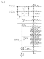
- FIG. 3 is a diagram illustrating the circuit principle of automatically adjust a charging voltage provided by the present disclosure
- FIG. 4 is a flowchart illustrating the charging control provided by the present disclosure.
- Embodiment 1 of the present disclosure provides a management device for a charging circuit.
- the management device for a charging circuit includes: a power supply management module, a buck switching voltage converter and a linear charging circuit.
- the power supply management module includes an adjustable LDO linear regulator and an ADC, wherein the output terminal of the adjustable LDO linear regulator of the power supply management module is connected with the feedback terminal of the buck switching voltage converter through a preset resistor.
- the input terminal of the ADC of the power supply management module is connected with the anode of a battery.
- the control terminal of the power supply management module is connected with the control terminal of the linear charging circuit.
- the output terminal of the buck switching voltage converter is connected with the input terminal of the linear charging circuit.
- the output terminal of the linear charging circuit is connected with the anode of the battery.
- the ADC of the power supply management module is configured to sample the battery power, and, when determining that the battery is effective and that the battery power is not full, feed back the output voltage of the adjustable LDO linear regulator to the buck switching voltage converter according to the voltage of the battery.
- the buck switching voltage converter is configured to output a voltage to the linear charging circuit according to the feedback result.
- the linear charging circuit is configured to charge the battery under the control of the power supply management module;
- Vfb is the voltage of the feedback terminal of the buck switching voltage converter
- V1 is the resistance value of a first preset resistor
- V2 is the resistance value of a second preset resistor
- V3 is the resistance value of a third preset resistor.
- the management device for a charging circuit includes a hardware circuit part and a software control part, wherein the hardware circuit part includes: a power supply management module, a buck switching voltage converter and a linear charging circuit;
- a conventional linear charging circuit includes a PNP charging tube, a sense resistor and a P type Metal-Oxide-Semiconductor (PMOS) control tube etc.
- the emitter of the PNP charging tube is the input terminal of the charging circuit and the voltage of the collector electrode is close to the voltage of the battery.
- the voltage drop on the PNP charging tube will be also relatively large, wherein the linear charging circuit as shown in FIG. 2 is only used as an example, but not intended to limit the protection scope of the present disclosure;
- the power supply management module includes an adjustable LDO linear regulator and an ADC, wherein a buck switching voltage converter is the core of the present disclosure.
- a buck switching voltage converter is the core of the present disclosure.
- the feedback terminal of the buck switching voltage converter is controlled by the output voltage of the adjustable LDO linear regulator in the power supply management module, thus realizing an adjustable output voltage.
- a Qualcomm PM7540-type power supply management module is used as an example in this embodiment, but not intended to limit the protection scope of the present disclosure.
- the output voltage of the adjustable LDO linear regulator of the power supply management module is set according to the voltage of the battery, thus forming a feedback control circuit.
- the output voltage of the buck switching voltage converter is adjusted in real time according to the voltage of the battery to charge the battery.
- the output voltage of the buck switching voltage converter which is automatically adjusted according to the voltage of the battery is usually about 0.3V higher than the voltage of the battery, and such output voltage can be taken as the input of the charging circuit.
- the sum of the voltage drop of the PMOS control tube and that of the sense resistor is about 0.1V and the maximum saturation voltage of the PNP charging tube can be 0.08V.
- the charging voltage is constantly 5V
- the voltage of a lithium battery is 3.7V
- the voltage drop on a charging circuit is about 1.3V.
- the normal operating voltage is within a range of 3.3V ⁇ 4.2V and the voltage drop on the PNP charging tube is within a dynamic range. What needs to be explained is that, the voltage different of 0.3V between the buck switching voltage converter and the charging circuit is only a preferred value, but not intended to limit the protection scope of the present disclosure.
- the buck switching voltage converter is the core of the present disclosure. As shown in FIG. 3 , a voltage converter with an adjustable output voltage is improved on the basis of a conventional buck switching voltage converter with fixed output.
- the control of the feedback terminal is the core of the circuit and forms a control system capable of automatically adjusting the charging voltage according to the voltage of the battery.
- the feedback voltage is influenced by the adjustable LDO output voltage (VBAT_CTRL) in the power supply management module together with the dynamic output voltage (VDC_OUT).
- An appropriate feedback resistor can be selected to acquire an appropriate range of the output voltage of a buck switching voltage converter chip.
- a voltage converter is based on a buck switching voltage converter with low cost and high efficiency, and description is given in this embodiment taking a Zi1153 buck switching voltage converter chip as an example.
- the chip is used in the following scenarios in the present disclosure: the input voltage is 5V ⁇ 10%, the output voltage is 3.5 ⁇ 4.4V, the output current is about 700 mA, and it can be learned from the device information that the power efficiency is above 90%.
- the threshold voltage of the feedback terminal is 0.6V (Vfb), the feedback input bias current is smaller than 30 nA which is equivalent to a virtual open circuit, and the output voltage is determined by a divider resistor. It can be seen from FIG.
- a resistor R 62 is added to control the feedback terminal.
- the voltage of one terminal of the resistor R 62 is output by an adjustable LDO regulator in the power supply management module, and the output voltage of the LDO regulator is set according to the voltage of the battery. Appropriate resistance values (with a precision of at least 1%) are selected for the three aforementioned resistors and the range of the output voltage of the buck switching voltage converter is able to meet the charging requirement.
- the resistance values of the resistor R 26 , resistor R 34 and resistor R 62 are 121K ohms, 19.1K ohms and 121 ohms, respectively. Since the input current of the feedback terminal of the buck switching voltage converter chip is smaller than 30 nA and the currents flowing through these three resistors are dozens of microamperes, the current flowing into the feedback terminal can be neglected.
- Vfb is the voltage of the feedback terminal of the buck switching voltage converter
- VR 26 is the resistance value of the resistor R 26
- VR 34 is the resistance value of the resistor R 34
- VR 62 is the resistance value of the resistor R 62 ;
- resistor R 62 is referred to as the first preset resistor
- R 34 is referred to as the second present resistor
- R 26 is referred to as the third preset resistor.
- the values of these resistors are not limited to the aforementioned values, and the value of Vfb depends on the used buck switching voltage converter chip.
- the output range of the adjustable LDO regulator is 0.75 ⁇ 1.5V, thus the output voltage of the buck switching voltage converter is determined accordingly. For example, if the output voltage of the adjustable LDO regulator is set as 1.5V, the output voltage of the buck switching voltage converter is 3.5V. If the output voltage of the adjustable LDO regulator is set as 0.75V, the output voltage of the buck switching voltage converter is 4.25V.
- the voltage of the battery is 3.2 ⁇ 3.95V, the battery can be set in a state of constant current charging, and the output voltage of the buck switching voltage converter is adjusted within 3.5 ⁇ 4.25V in this case.
- the voltage of the battery is 3.95 ⁇ 4.2V, the battery can be set in a state of constant voltage charging or pulse charging, the output of the adjustable LDO regulator in the charging state is turned off in this case, which means that the adjustable LDO regulator is disconnected from the feedback terminal of the buck switching voltage converter.
- the output voltage of the buck switching voltage converter is 4.4V, which satisfies the requirement of turning-on.
- the adjustable output voltage of the buck switching voltage converter needs to be realized by software control, and the software control process is shown in FIG. 4 .
- the software control process is shown in FIG. 4 .
- the ADC of the power supply management module detects the battery ID and samples the voltage of the battery (step S 1 ).
- step S 2 If the ID is valid and the battery power is not full, the output voltage of the adjustable LDO regulator is set according to the voltage of the battery (step S 2 ), and change of the output voltage of the adjustable LDO regulator is fed back to the buck switching voltage converter to complete the automatic adjustment of the output voltage of the buck switching voltage converter (step S 4 ). Subsequently, it is detected whether the charging current and the charging voltage are within an allowable range (step S 5 ).
- step S 7 If the charging current and the charging voltage are normal, the battery is charged normally (step S 7 ), the voltage of the battery continues to increase, the output voltage of the adjustable LDO regulator is set to be decreased gradually, and the corresponding relation between the set output voltage of the adjustable LDO regulator and the output voltage of the buck switching voltage converter is shown in Table 1 to facilitate realization of programming.
- the output of the adjustable LDO regulator is turned off to ensure that the whole machine supplies power to the external equipment and does not consume the battery power, which is good for the battery life and safety.
- the buck switching voltage converter outputs a constant voltage (step S 3 ), and then charging is completed or terminated abnormally (step S 6 ).
- the voltage of the battery is variable, and the output of the adjustable LDO regulator changes accordingly, thus the output voltage of the buck switching voltage converter is automatically adjusted, so that the charging voltage is higher than the voltage of the battery and a certain difference is maintained, in this way, the charging requirement is satisfied while loss of the PNP charging tube is reduced, and the highest charging efficiency can be achieved in the whole charging system.
- the emerging MIFI products can work while being charged for a long time.
- Miniaturization of products present a challenge for the whole dissipated heat and the best method to solve the problem of heat dissipation of terminal products is to reduce the whole power consumption.
- the whole heat dissipation can be effectively reduced using the charging circuit of the present disclosure, along with another advantage: the operating current of an MIFI product is above 600 mA in the worst case, since the current output capability of the USB interface is 500 mA, thus, the current will be insufficient if a USB is used to supply power to a conventional charging circuit.
- the battery will discharge if the current supplied to the external equipment is insufficient, the output voltage of the buck switching voltage converter will decrease along with the resulting decrease in the voltage of the battery, and generally, an automatic turning-off will occur if the voltage of the battery is lower than 3.3V.
- normal work can be ensured only when the output voltage of the buck switching voltage converter is at least 3.6V.
- Embodiment 2 of the present disclosure further provides a wireless terminal, including: a charging circuit management device.
- the charging circuit management device includes: a power supply management module, a buck switching voltage converter and a linear charging circuit.
- the power supply management module includes an adjustable LDO linear regulator and an ADC, wherein the output terminal of the adjustable LDO linear regulator of the power supply management module is connected with the feedback terminal of the buck switching voltage converter through a first preset resistor.
- the input terminal of the ADC of the power supply management module is connected with the anode of a battery.
- the control terminal of the power supply management module is connected with the control terminal of the linear charging circuit.
- the output terminal of the buck switching voltage converter is connected with the input terminal of the linear charging circuit.
- the output terminal of the linear charging circuit is connected with the anode of the battery.
- the ADC of the power supply management module is configured to sample the battery power, and when determining that the battery is effective and that the battery power is not full, feed back the output voltage of the adjustable LDO linear regulator to the buck switching voltage converter according to the voltage of the battery.
- the buck switching voltage converter is configured to output a voltage to the linear charging circuit according to the feedback result.
- the linear charging circuit is configured to charge the battery under the control of the power supply management module.
- Vfb is the voltage of the feedback terminal of the buck switching voltage converter
- V1 is the resistance value of the first preset resistor
- V2 is the resistance value of a second preset resistor
- V3 is the resistance value of a third preset resistor.
- the present disclosure can realize automatic adjustment of the charging voltage by adding a buck switching voltage converter and utilizing an adjustable LDO linear regulator in a power supply management module, thus reducing the voltage drop on the charging tube (i.e. reducing the energy loss), the whole power loss is reduced to improve the whole heat dissipation well.
Landscapes
- Engineering & Computer Science (AREA)
- Power Engineering (AREA)
- Charge And Discharge Circuits For Batteries Or The Like (AREA)
- Secondary Cells (AREA)
- Dc-Dc Converters (AREA)
Applications Claiming Priority (4)
| Application Number | Priority Date | Filing Date | Title |
|---|---|---|---|
| CN201010239150.X | 2010-07-23 | ||
| CN201010239150 | 2010-07-23 | ||
| CN201010239150.XA CN101902043B (zh) | 2010-07-23 | 2010-07-23 | 充电电路管理装置及无线终端 |
| PCT/CN2010/080385 WO2012009935A1 (fr) | 2010-07-23 | 2010-12-28 | Dispositif de gestion pour circuit de charge et terminal sans fil |
Publications (2)
| Publication Number | Publication Date |
|---|---|
| US20120319643A1 US20120319643A1 (en) | 2012-12-20 |
| US8378626B2 true US8378626B2 (en) | 2013-02-19 |
Family
ID=43227340
Family Applications (1)
| Application Number | Title | Priority Date | Filing Date |
|---|---|---|---|
| US13/580,151 Active US8378626B2 (en) | 2010-07-23 | 2010-12-28 | Management device for charging circuit and wireless terminal |
Country Status (4)
| Country | Link |
|---|---|
| US (1) | US8378626B2 (fr) |
| EP (1) | EP2528186B1 (fr) |
| CN (1) | CN101902043B (fr) |
| WO (1) | WO2012009935A1 (fr) |
Cited By (6)
| Publication number | Priority date | Publication date | Assignee | Title |
|---|---|---|---|---|
| TWI580152B (zh) * | 2014-11-08 | 2017-04-21 | 立錡科技股份有限公司 | 高效率充電系統與應用於其中之充電電路 |
| US9973017B2 (en) | 2014-09-19 | 2018-05-15 | Samsung Electronics Co., Ltd. | Charger circuit including a plurality of charging paths |
| US20220216721A1 (en) * | 2019-09-29 | 2022-07-07 | Autel Intelligent Technology Corp., Ltd. | Control system and method for improving battery output energy efficiency, and electronic device |
| US20220239121A1 (en) * | 2021-01-28 | 2022-07-28 | Contemporary Amperex Technology Co., Limited | Charging method, battery management system of traction battery and charging pile |
| US20220239140A1 (en) * | 2021-01-28 | 2022-07-28 | Contemporary Amperex Technology Co., Limited | Charging method and power conversion apparatus |
| US12095301B2 (en) * | 2021-01-28 | 2024-09-17 | Contemporary Amperex Technology Co., Limited | Pulse charging method, battery management system of traction battery and charging pile |
Families Citing this family (18)
| Publication number | Priority date | Publication date | Assignee | Title |
|---|---|---|---|---|
| CN101902043B (zh) * | 2010-07-23 | 2014-06-04 | 中兴通讯股份有限公司 | 充电电路管理装置及无线终端 |
| CN102075088B (zh) * | 2011-01-31 | 2014-10-29 | 复旦大学 | 一种开关电压转换器和线性稳压器级联的方法 |
| CN102185348A (zh) * | 2011-04-28 | 2011-09-14 | 天津理工大学 | 微电能收集及转换电路器 |
| CN102891923A (zh) * | 2011-07-25 | 2013-01-23 | 深圳市福智软件技术有限公司 | 移动终端及其电源自动切换方法 |
| CN102291489B (zh) * | 2011-08-10 | 2014-11-05 | 惠州Tcl移动通信有限公司 | 手机及其电压校准方法 |
| CN103647318B (zh) * | 2013-12-04 | 2016-03-02 | 华为终端有限公司 | 通讯终端、充电控制方法、装置及电路 |
| DE102015221101B4 (de) | 2015-10-28 | 2022-12-08 | Dialog Semiconductor (Uk) Limited | Batterieladeregler, Ladegerät zum Laden einer Batterie, tragbare elektronische Vorrichtung mit Ladegerät und Verfahren für einen Betrieb eines Ladegeräts |
| CN105391286B (zh) * | 2015-11-06 | 2018-05-01 | 上海斐讯数据通信技术有限公司 | 一种基于高通平台的电源供电电路 |
| AU2018249241B2 (en) * | 2017-04-07 | 2020-07-16 | Guangdong Oppo Mobile Telecommunications Corp., Ltd. | Wireless charging apparatus, device to be charged and control method therefor |
| JP6938810B2 (ja) * | 2017-09-26 | 2021-09-22 | 株式会社三社電機製作所 | 検査装置 |
| EP3745554A4 (fr) * | 2018-04-25 | 2021-02-17 | Guangdong Oppo Mobile Telecommunications Corp., Ltd. | Dispositif terminal et procédé de commande de charge |
| CN108896911B (zh) * | 2018-04-26 | 2021-04-30 | 广东小天才科技有限公司 | 一种电子设备的充电异常检测方法及装置 |
| CN108720797A (zh) * | 2018-05-30 | 2018-11-02 | 山东煜和堂药业有限公司 | 可视喉镜开关机、插入充电器自动开机及视频供电电路 |
| CN110718944B (zh) * | 2018-07-12 | 2023-08-04 | 中兴通讯股份有限公司 | 一种双电池充放电的方法、装置、终端和存储介质 |
| US10969809B2 (en) * | 2018-08-02 | 2021-04-06 | Microchip Technology Incorporated | Dual input LDO voltage regulator |
| CN110601310B (zh) * | 2019-09-30 | 2024-06-11 | 江门嘉权知识产权运营有限公司 | 一种基于锂电池供电的多电压输出电源装置 |
| CN112968498A (zh) * | 2021-03-11 | 2021-06-15 | 成都芯源系统有限公司 | 从充电系统接收供电的方法及充电系统 |
| CN115378078B (zh) * | 2022-08-23 | 2025-07-29 | 安徽皖仪科技股份有限公司 | 一种低压直流充电的铅酸电池充电系统及方法 |
Citations (13)
| Publication number | Priority date | Publication date | Assignee | Title |
|---|---|---|---|---|
| US5701068A (en) * | 1995-04-03 | 1997-12-23 | Electrosource, Inc. | Battery management system |
| US6239509B1 (en) * | 1999-07-16 | 2001-05-29 | Semtech Corporation | Method and apparatus for voltage regulation in multi-output switched mode power supplies |
| US6259234B1 (en) * | 1998-04-15 | 2001-07-10 | Agence Spatiale Europeenne | Converter module for an electrical power supply and a system including it |
| US6348744B1 (en) * | 1998-04-14 | 2002-02-19 | Conexant Systems, Inc. | Integrated power management module |
| US20020093318A1 (en) * | 2000-11-22 | 2002-07-18 | Mark Wallis | Apparatus and method for controlling voltage regulator and power supply apparatus |
| US20050040800A1 (en) * | 2003-08-21 | 2005-02-24 | Sehat Sutardja | Digital low dropout regulator |
| US7064531B1 (en) * | 2005-03-31 | 2006-06-20 | Micrel, Inc. | PWM buck regulator with LDO standby mode |
| US7145316B1 (en) * | 2005-06-06 | 2006-12-05 | Micrel, Inc. | Control circuit for monitoring and maintaining a bootstrap voltage in an N-channel buck regulator |
| US20070252564A1 (en) * | 2006-04-14 | 2007-11-01 | Atmel Corporation | Method and circuit for a voltage supply for real time clock circuitry based on voltage regulated charge pump |
| CN101154821A (zh) | 2007-09-21 | 2008-04-02 | 中兴通讯股份有限公司 | 一种用于镍氢电池的快速充电装置及方法 |
| US20090021228A1 (en) | 2007-07-20 | 2009-01-22 | Frank Carr | Integrated cmos dc-dc converter implementation in low-voltage cmos technology using ldo regulator |
| US20090153108A1 (en) | 2007-12-17 | 2009-06-18 | Neil Hendin | Power management efficiency using DC-DC and linear regulators in conjunction |
| CN101902043A (zh) | 2010-07-23 | 2010-12-01 | 中兴通讯股份有限公司 | 充电电路管理装置及无线终端 |
Family Cites Families (3)
| Publication number | Priority date | Publication date | Assignee | Title |
|---|---|---|---|---|
| CN100392942C (zh) * | 2005-10-31 | 2008-06-04 | 中兴通讯股份有限公司 | 一种对电池充电过程进行控制的装置及方法 |
| US20080100143A1 (en) * | 2006-11-01 | 2008-05-01 | O2Micro Inc. | Power management system with charger/boost controller |
| US7834600B2 (en) * | 2006-12-14 | 2010-11-16 | Linear Technology Corporation | Regulated power supply system and an operating method therefore |
-
2010
- 2010-07-23 CN CN201010239150.XA patent/CN101902043B/zh not_active Expired - Fee Related
- 2010-12-28 EP EP10854965.0A patent/EP2528186B1/fr not_active Not-in-force
- 2010-12-28 WO PCT/CN2010/080385 patent/WO2012009935A1/fr not_active Ceased
- 2010-12-28 US US13/580,151 patent/US8378626B2/en active Active
Patent Citations (16)
| Publication number | Priority date | Publication date | Assignee | Title |
|---|---|---|---|---|
| US5701068A (en) * | 1995-04-03 | 1997-12-23 | Electrosource, Inc. | Battery management system |
| US6348744B1 (en) * | 1998-04-14 | 2002-02-19 | Conexant Systems, Inc. | Integrated power management module |
| US6259234B1 (en) * | 1998-04-15 | 2001-07-10 | Agence Spatiale Europeenne | Converter module for an electrical power supply and a system including it |
| US6239509B1 (en) * | 1999-07-16 | 2001-05-29 | Semtech Corporation | Method and apparatus for voltage regulation in multi-output switched mode power supplies |
| US20020093318A1 (en) * | 2000-11-22 | 2002-07-18 | Mark Wallis | Apparatus and method for controlling voltage regulator and power supply apparatus |
| US20050040800A1 (en) * | 2003-08-21 | 2005-02-24 | Sehat Sutardja | Digital low dropout regulator |
| US7064531B1 (en) * | 2005-03-31 | 2006-06-20 | Micrel, Inc. | PWM buck regulator with LDO standby mode |
| US7145316B1 (en) * | 2005-06-06 | 2006-12-05 | Micrel, Inc. | Control circuit for monitoring and maintaining a bootstrap voltage in an N-channel buck regulator |
| US20070252564A1 (en) * | 2006-04-14 | 2007-11-01 | Atmel Corporation | Method and circuit for a voltage supply for real time clock circuitry based on voltage regulated charge pump |
| US7550954B2 (en) | 2006-04-14 | 2009-06-23 | Atmel Corporation | Method and circuit for a voltage supply for real time clock circuitry based on voltage regulated charge pump |
| US20090021228A1 (en) | 2007-07-20 | 2009-01-22 | Frank Carr | Integrated cmos dc-dc converter implementation in low-voltage cmos technology using ldo regulator |
| US7728550B2 (en) | 2007-07-20 | 2010-06-01 | Newport Media, Inc. | Integrated CMOS DC-DC converter implementation in low-voltage CMOS technology using LDO regulator |
| CN101154821A (zh) | 2007-09-21 | 2008-04-02 | 中兴通讯股份有限公司 | 一种用于镍氢电池的快速充电装置及方法 |
| US20090153108A1 (en) | 2007-12-17 | 2009-06-18 | Neil Hendin | Power management efficiency using DC-DC and linear regulators in conjunction |
| TW200937161A (en) | 2007-12-17 | 2009-09-01 | Nvidia Corp | Improved power management efficiency using DC-DC and linear regulators in conjunction |
| CN101902043A (zh) | 2010-07-23 | 2010-12-01 | 中兴通讯股份有限公司 | 充电电路管理装置及无线终端 |
Non-Patent Citations (2)
| Title |
|---|
| English Translation of the Written Opinion of the International Search Authority in international application No. PCT/CN2010/080385, mailed on May 5, 2011. |
| International Search Report in international application No. PCT/CN2010/080385, mailed on May 5, 2011. |
Cited By (9)
| Publication number | Priority date | Publication date | Assignee | Title |
|---|---|---|---|---|
| US9973017B2 (en) | 2014-09-19 | 2018-05-15 | Samsung Electronics Co., Ltd. | Charger circuit including a plurality of charging paths |
| TWI580152B (zh) * | 2014-11-08 | 2017-04-21 | 立錡科技股份有限公司 | 高效率充電系統與應用於其中之充電電路 |
| US20220216721A1 (en) * | 2019-09-29 | 2022-07-07 | Autel Intelligent Technology Corp., Ltd. | Control system and method for improving battery output energy efficiency, and electronic device |
| US12451716B2 (en) * | 2019-09-29 | 2025-10-21 | Autel Intelligent Technology Corp., Ltd. | Control system and method for improving battery output energy efficiency, and electronic device |
| US20220239121A1 (en) * | 2021-01-28 | 2022-07-28 | Contemporary Amperex Technology Co., Limited | Charging method, battery management system of traction battery and charging pile |
| US20220239140A1 (en) * | 2021-01-28 | 2022-07-28 | Contemporary Amperex Technology Co., Limited | Charging method and power conversion apparatus |
| US12095301B2 (en) * | 2021-01-28 | 2024-09-17 | Contemporary Amperex Technology Co., Limited | Pulse charging method, battery management system of traction battery and charging pile |
| US12374916B2 (en) * | 2021-01-28 | 2025-07-29 | Contemporary Amperex Technology (Hong Kong) Limited | Charging method and power conversion apparatus |
| US12401203B2 (en) * | 2021-01-28 | 2025-08-26 | Contemporary Amperex Technology (Hong Kong) Limited | Charging method, battery management system of traction battery and charging pile |
Also Published As
| Publication number | Publication date |
|---|---|
| WO2012009935A1 (fr) | 2012-01-26 |
| CN101902043A (zh) | 2010-12-01 |
| EP2528186A4 (fr) | 2013-10-09 |
| US20120319643A1 (en) | 2012-12-20 |
| EP2528186B1 (fr) | 2014-08-13 |
| CN101902043B (zh) | 2014-06-04 |
| EP2528186A1 (fr) | 2012-11-28 |
Similar Documents
| Publication | Publication Date | Title |
|---|---|---|
| US8378626B2 (en) | Management device for charging circuit and wireless terminal | |
| Muniandi et al. | A 97% maximum efficiency fully automated control turbo boost topology for battery chargers | |
| US10804738B2 (en) | Multipath charger and charging method thereof | |
| KR102418710B1 (ko) | 충전 장치 및 단말 | |
| US9490644B2 (en) | Reconfigurable compensator with large-signal stabilizing network | |
| US8405362B2 (en) | Method and system for minimum output-voltage battery charger | |
| US20180278068A1 (en) | Electronic device and power adapter therefor | |
| CN113078699A (zh) | 一种终端及其供电方法、充放电管理电路 | |
| CN109510272B (zh) | 一种充电控制方法及充电电路 | |
| US20210376643A1 (en) | Adaptive Power Systems and Techniques | |
| CN103647318B (zh) | 通讯终端、充电控制方法、装置及电路 | |
| US20230275452A1 (en) | Power system, charging method, and discharging method | |
| US20220181890A1 (en) | Charging system and method | |
| US20180145525A1 (en) | Charging managment method and system thereof | |
| WO2022036667A1 (fr) | Circuit de commande de cellule, et dispositif électronique | |
| US20170222453A1 (en) | Device, apparatus and method for supporting multi-battery quick charge | |
| CN101950993A (zh) | 一种锂电池充电器和直流稳压电源集成电路系统 | |
| JP7768965B2 (ja) | 電力システム | |
| CN211930261U (zh) | 一种供电线缆组件 | |
| CN220914981U (zh) | 镍氢电池组的充电电路、电源装置及车辆 | |
| US20230045028A1 (en) | Charging system, method and device for controlling charging system, and electronic device | |
| CN117833427A (zh) | 电量调整电路及电子设备 | |
| US20250125724A1 (en) | Hybrid buck converter and operating method thereof | |
| CN211018347U (zh) | 一种多口充电设备 | |
| KR102886621B1 (ko) | 스마트 리니어 배터리 충전 시스템 |
Legal Events
| Date | Code | Title | Description |
|---|---|---|---|
| AS | Assignment |
Owner name: ZTE CORPORATION, CHINA Free format text: ASSIGNMENT OF ASSIGNORS INTEREST;ASSIGNOR:WANG, JIHONG;REEL/FRAME:028873/0010 Effective date: 20120509 |
|
| STCF | Information on status: patent grant |
Free format text: PATENTED CASE |
|
| FPAY | Fee payment |
Year of fee payment: 4 |
|
| MAFP | Maintenance fee payment |
Free format text: PAYMENT OF MAINTENANCE FEE, 8TH YEAR, LARGE ENTITY (ORIGINAL EVENT CODE: M1552); ENTITY STATUS OF PATENT OWNER: LARGE ENTITY Year of fee payment: 8 |
|
| MAFP | Maintenance fee payment |
Free format text: PAYMENT OF MAINTENANCE FEE, 12TH YEAR, LARGE ENTITY (ORIGINAL EVENT CODE: M1553); ENTITY STATUS OF PATENT OWNER: LARGE ENTITY Year of fee payment: 12 |