US8559199B2 - Power factor correction circuit for three-phase power supply - Google Patents
Power factor correction circuit for three-phase power supply Download PDFInfo
- Publication number
- US8559199B2 US8559199B2 US12/809,994 US80999408A US8559199B2 US 8559199 B2 US8559199 B2 US 8559199B2 US 80999408 A US80999408 A US 80999408A US 8559199 B2 US8559199 B2 US 8559199B2
- Authority
- US
- United States
- Prior art keywords
- mode
- current
- differential
- correction circuit
- inductors
- Prior art date
- Legal status (The legal status is an assumption and is not a legal conclusion. Google has not performed a legal analysis and makes no representation as to the accuracy of the status listed.)
- Active, expires
Links
- 238000001914 filtration Methods 0.000 claims abstract description 112
- 230000001939 inductive effect Effects 0.000 claims abstract description 29
- 238000004804 winding Methods 0.000 claims abstract description 16
- 239000000696 magnetic material Substances 0.000 claims abstract description 3
- 239000011347 resin Substances 0.000 claims description 4
- 229920005989 resin Polymers 0.000 claims description 4
- 239000000463 material Substances 0.000 claims description 2
- 229910000859 α-Fe Inorganic materials 0.000 claims description 2
- 239000003990 capacitor Substances 0.000 description 22
- 238000005457 optimization Methods 0.000 description 4
- 230000000593 degrading effect Effects 0.000 description 3
- 230000005540 biological transmission Effects 0.000 description 2
- 230000007123 defense Effects 0.000 description 2
- 238000010586 diagram Methods 0.000 description 2
- 230000007935 neutral effect Effects 0.000 description 2
- 230000002238 attenuated effect Effects 0.000 description 1
- 230000015556 catabolic process Effects 0.000 description 1
- 238000006243 chemical reaction Methods 0.000 description 1
- 238000006731 degradation reaction Methods 0.000 description 1
- 230000003292 diminished effect Effects 0.000 description 1
- 238000007599 discharging Methods 0.000 description 1
- 230000005669 field effect Effects 0.000 description 1
- 238000009499 grossing Methods 0.000 description 1
- 238000002955 isolation Methods 0.000 description 1
- 238000004519 manufacturing process Methods 0.000 description 1
- 238000005259 measurement Methods 0.000 description 1
- 229910044991 metal oxide Inorganic materials 0.000 description 1
- 150000004706 metal oxides Chemical class 0.000 description 1
- 229910000595 mu-metal Inorganic materials 0.000 description 1
- 238000000819 phase cycle Methods 0.000 description 1
- 230000010363 phase shift Effects 0.000 description 1
- 239000004065 semiconductor Substances 0.000 description 1
- 230000035939 shock Effects 0.000 description 1
- 239000013589 supplement Substances 0.000 description 1
- 230000001052 transient effect Effects 0.000 description 1
Images




Classifications
-
- H—ELECTRICITY
- H02—GENERATION; CONVERSION OR DISTRIBUTION OF ELECTRIC POWER
- H02M—APPARATUS FOR CONVERSION BETWEEN AC AND AC, BETWEEN AC AND DC, OR BETWEEN DC AND DC, AND FOR USE WITH MAINS OR SIMILAR POWER SUPPLY SYSTEMS; CONVERSION OF DC OR AC INPUT POWER INTO SURGE OUTPUT POWER; CONTROL OR REGULATION THEREOF
- H02M1/00—Details of apparatus for conversion
- H02M1/42—Circuits or arrangements for compensating for or adjusting power factor in converters or inverters
- H02M1/4208—Arrangements for improving power factor of AC input
- H02M1/4216—Arrangements for improving power factor of AC input operating from a three-phase input voltage
-
- H—ELECTRICITY
- H02—GENERATION; CONVERSION OR DISTRIBUTION OF ELECTRIC POWER
- H02M—APPARATUS FOR CONVERSION BETWEEN AC AND AC, BETWEEN AC AND DC, OR BETWEEN DC AND DC, AND FOR USE WITH MAINS OR SIMILAR POWER SUPPLY SYSTEMS; CONVERSION OF DC OR AC INPUT POWER INTO SURGE OUTPUT POWER; CONTROL OR REGULATION THEREOF
- H02M1/00—Details of apparatus for conversion
- H02M1/12—Arrangements for reducing harmonics from AC input or output
- H02M1/126—Arrangements for reducing harmonics from AC input or output using passive filters
-
- H—ELECTRICITY
- H02—GENERATION; CONVERSION OR DISTRIBUTION OF ELECTRIC POWER
- H02M—APPARATUS FOR CONVERSION BETWEEN AC AND AC, BETWEEN AC AND DC, OR BETWEEN DC AND DC, AND FOR USE WITH MAINS OR SIMILAR POWER SUPPLY SYSTEMS; CONVERSION OF DC OR AC INPUT POWER INTO SURGE OUTPUT POWER; CONTROL OR REGULATION THEREOF
- H02M1/00—Details of apparatus for conversion
- H02M1/44—Circuits or arrangements for compensating for electromagnetic interference in converters or inverters
-
- Y—GENERAL TAGGING OF NEW TECHNOLOGICAL DEVELOPMENTS; GENERAL TAGGING OF CROSS-SECTIONAL TECHNOLOGIES SPANNING OVER SEVERAL SECTIONS OF THE IPC; TECHNICAL SUBJECTS COVERED BY FORMER USPC CROSS-REFERENCE ART COLLECTIONS [XRACs] AND DIGESTS
- Y02—TECHNOLOGIES OR APPLICATIONS FOR MITIGATION OR ADAPTATION AGAINST CLIMATE CHANGE
- Y02B—CLIMATE CHANGE MITIGATION TECHNOLOGIES RELATED TO BUILDINGS, e.g. HOUSING, HOUSE APPLIANCES OR RELATED END-USER APPLICATIONS
- Y02B70/00—Technologies for an efficient end-user side electric power management and consumption
- Y02B70/10—Technologies improving the efficiency by using switched-mode power supplies [SMPS], i.e. efficient power electronics conversion e.g. power factor correction or reduction of losses in power supplies or efficient standby modes
Definitions
- the present invention relates to a power-factor correction circuit for a three-phase power supply.
- the invention applies notably to the field of power electronics, in particular the production of three-phase power supply units.
- a power electronic circuit sometimes introduces a reactive power causing a phase shift of the power supply current and voltage.
- one or more conversion stages present in said electronic circuit for example a stage for rectifying the voltage, cause deformations of the input current, consequently degrading the power factor.
- the power electronic circuit therefore requires, at its input, the addition of a correction circuit in order to increase the power factor.
- the correction circuit indicated by the acronym PFC in the rest of the description with reference to the expression “Power Factor Correction” must put the current and the voltage back into phase.
- the PFC circuit must limit the harmonic distortions of the input current. Therefore, a PFC circuit must at least meet two constraints simultaneously: obtain a high power factor and a good quality of the induced-current harmonic distortion.
- the new standards, notably concerning purity in current shape are increasingly strict, as shown, for example, by the chapters relating to conducted emissions of the MIL-STD-461E standard of the American Defense Department.
- FIG. 1 An alternative solution using the principle of the PFC circuits of the “boost” type is shown in FIG. 1 .
- It is a conventional correction circuit 100 for a three-phase power supply comprising a first filtering unit 101 dedicated to the low frequencies, a hexaphase rectifying bridge 102 , a second filtering unit 103 dedicated to the high frequencies, and a voltage step-up stage 104 , which comprises an inductor 105 , a controlled switch 106 , and a freewheel diode 107 powering a reservoir capacitor C.
- the value of the inductor 105 is chosen to be sufficiently large for the circuit 100 to operate in continuous mode.
- the capacitor C is a reserve of energy making it possible to power a user circuit, modeled in FIG. 1 by a load 110 .
- This conventional correction circuit 100 makes it possible, without having recourse to three PFC stages, to significantly increase the power factor of the circuit.
- the inductor 105 since the value of the inductor 105 has to be high to obtain an acceptable smoothing of the current, the inductive component chosen to fulfill this role is often very bulky.
- the architecture of this circuit shows its limits in quality of the harmonic distortions; it does not make it possible to satisfy the requirements of the strictest standards.
- the subject of the invention is a correction circuit of the power factor of a circuit for a three-phase electric network comprising a filtering unit at the input receiving the three phases of the current, at least one inductor per phase placed downstream of the filtering unit, a rectifying bridge powering a current-chopping stage, characterized in that the filtering unit comprises a differential-mode filtering cell comprising at least one inductive circuit formed of a single magnetic material in a double E, each leg of the E being surrounded by a winding, the values of the inductors being chosen so that said correction circuit operates at the boundary between the continuous mode and the discontinuous mode.
- the filtering unit comprises a first common-mode filtering cell, associated in series with a first differential-mode filtering cell and a second differential-mode filtering cell, the filtering unit also comprising a second common-mode filtering cell comprising a mid-point output and inserted between the first differential-mode filtering cell and the second differential-mode filtering cell.
- the second differential-mode filtering cell comprises simple inductors and the assembly of the differential-mode inductors is incorporated into a molded resin block, said assembly consisting of the inductive modules and of the simple inductors of the first differential-mode filtering cell and of the simple inductors of the second differential-mode filtering cell.
- a further subject of the invention is a power supply unit comprising a power-factor correction circuit as described above.
- the circuit according to the invention is unitary, that is to say that it comprises a single PFC circuit operating in three-phase mode.
- This feature has several advantages. On the one hand, it makes it possible to reduce the overall size of the circuit by a factor of 3. On the other hand, it makes it possible to solve the problems of balancing the phases, whether or not the neutral of the three-phase network is connected to the circuit. Moreover, an additional architecture requiring computing modules such as a DSP or a CPLD is no longer necessary.
- FIG. 1 a correction circuit architecture according to the prior art, the figure has already been explained
- FIG. 2 the architecture of an embodiment of a correction circuit optimized according to the invention
- FIG. 3 a the illustration of the first phase of the current-chopping cycle carried out by a correction circuit according to the invention
- FIG. 4 a the shape of the current I LS passing through an inductor of the correction circuit according to the invention, and an illustration of the shape of the phase current I PH obtained with said circuit, after an optimization of the inductor value,
- FIG. 4 b a closer view of the inductor current I LS shown in FIG. 4 a
- FIG. 4 c an illustration of the shape of the phase current I PH obtained with a correction circuit according to the invention
- FIG. 5 a schematic diagram of a filtering unit contained in a correction circuit according to the invention
- FIG. 6 a a top view of a filtering unit contained in a correction circuit according to the invention
- FIG. 6 b two sections, in side view, of a filtering unit contained in a correction circuit according to the invention
- FIG. 7 a a top view of an inductive module present in the filtering module of a correction circuit according to the invention
- FIG. 7 b a side view of an inductive module present in the filtering module of a correction circuit according to the invention.
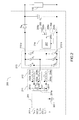
- FIG. 2 shows the architecture of an embodiment of the correction circuit according to the invention.
- the correction circuit 200 of FIG. 2 comprises a filtering unit 201 comprising three inputs 201 a , 201 b , 201 c and three outputs 201 d , 201 e , 201 f .
- the filtering unit 201 is powered by three current phases, a first phase V R on the first input 201 a , a second phase V S on the second input 201 b , and a third phase V T on the third input 201 c .
- the filtering unit 201 is connected to ground 201 t . This filtering unit 201 will be explained in detail below in FIGS. 3 , 5 , 6 a and 6 b.
- a filtering stage 211 making it possible to reject high-frequency components generated by the chopping of the current carried out by the PFC stage 214 described below, is placed in series at the output of the filtering unit 201 . More precisely, in the example of FIG. 2 , the first output 201 d of the filtering unit 201 is connected to its second output 201 e via a first capacitor C RS , its second output 201 e is connected to its third output 201 f via a second capacitor C ST , and its third output 201 f is connected to its first output 201 d via a third capacitor C RT . According to another embodiment, the high-frequency filtering stage 211 is incorporated into the filtering unit 201 .
- An inductive stage 212 is placed at the output of the high-frequency signal filtering stage 211 . More precisely, in the example of FIG. 2 , the first output 201 e of the filtering unit 201 is connected to the first terminal 202 a of a first inductor L R ; the second output 201 e of the filtering unit 201 is connected to the first terminal 203 a of a second inductor L S ; the third output 201 f of the filtering unit 201 is connected to the first terminal 204 a of a third inductor L T .
- the inductors L R , L S and L T are connected to a diode bridge 213 for rectifying the voltage. More precisely, in the example of FIG. 2 , the second terminal 202 b of the first inductor L R is connected to the anode of a first diode D 1 ; the second terminal 203 b of the second inductor L S is connected to the anode of a second diode D 2 ; the second terminal 204 b of the third inductor L T is connected to the anode of a third diode D 3 .
- the anode of the first diode is connected to the cathode of a fourth diode D 4 ; the anode of the second diode D 2 is connected to the cathode of a fifth diode D 5 ; the anode of the third diode is connected to the cathode of a sixth diode D 6 .
- the diode bridge 213 comprises two outputs 213 a , 213 b .
- the cathodes of the first diode D 1 , of the second diode D 2 and of the third diode D 3 are connected together at the first output 213 a of the diode bridge 213 .
- the anodes of the fourth diode D 4 , of the fifth diode D 5 and of the sixth diode D 6 are connected together at the second output 213 b of the diode bridge 213 .
- the first output 213 a of the diode bridge 213 is connected to the second output 213 b via a controlled switch 214 .
- the controlled switch 214 is formed by an MOSFET (Metal Oxide Semiconductor Field Effect Transistor) transistor 205 the drain 205 a of which is connected to the first output 213 a of the diode bridge 213 , the source 205 b of which is connected to the first terminal 206 a of a shunt resistor 206 , and the gate 205 c of which is controlled by a chopping signal generator 207 .
- MOSFET Metal Oxide Semiconductor Field Effect Transistor
- this generator 207 is a pulse width modulation generator, a signal at the low state causing a disabling of the MOSFET 205 , a signal at the high state controlling the flow of the current through the MOSFET 205 .
- the frequency of transmission of said pulses is very much higher than the frequency of the current originating from each of the input phases V R , V S and V T .
- the frequency of transmission of the pulses is of the order of 125 kHz for a network current at 400 Hz.
- the second terminal 206 b of the shunt resistor 206 is connected to the second output 213 b of the diode bridge 213 . This resistor 206 of very low value makes it possible to measure the current originating from the source 205 b of the MOSFET 205 in order to adapt the width of the pulses transmitted by the generator 207 .
- a freewheel diode D RL is placed so that its anode is connected to the first output 213 a of the diode bridge 213 and to the drain 205 a of the transistor 205 .
- a reservoir capacitor Cs is placed at the end of the circuit in order to store the energy necessary for the user circuit 110 to be powered, including in the event of a transient cut-out of the input AC network; the first terminal of this capacitor Cs being connected to the cathode of the freewheel diode D RL , the second terminal of this capacitor being connected to the second output 213 b of the diode bridge 213 .
- the correction circuit of FIG. 2 operates according to a two-phase cycle: a first phase during which the controlled switch 214 is closed, and a second phase during which the controlled switch 214 is open.
- the first phase is illustrated in FIG. 3 a .
- the controlled switch 214 being closed, a short circuit is formed at the branch comprised between the first output 213 a of the diode bridge 213 and its second output 213 b .
- the current shown in FIG. 3 a by an arrow Fi, therefore flows through this branch 213 a , 213 b as a short circuit and allows the inductors L R , L S , L T to store magnetic energy.
- the freewheel diode D RL is disabled and the current passing through said diode D RL is zero.
- the values of the inductors L R , L S and L T are optimized in order to limit the need for low-frequency signal filtering carried out by the filtering unit 201 , without degrading the input-current harmonic distortion.
- the values of the inductors L R , L S , L T are preferably chosen so that the correction circuit 200 operates at the boundary between the continuous mode and the discontinuous mode, in other words, the inductors L R , L S , L T finish discharging at the moment of beginning the first phase of the cycle.
- the lower the value of each of the inductors L R , L S , L T the more attenuated must be the inversion of the high-frequency current originating from the chopping carried out by the controlled switch 214 in order to maintain the high-frequency conducted emission requirements and hence the greater must be the attenuation of the filtering carried out by the filtering unit 201 in order to limit the harmonic distortions of the input current.
- the higher the value of the inductors L R , L S and L T the higher the risk of degrading the low-frequency harmonic distortion (that is to say the frequency of the network and its near harmonics). If the values for the inductors L R , L S and L T are too high, they would lead to a degradation of the envelope signal of the input current. Then, in order to preserve the shape of this envelope signal, it would be necessary to significantly increase the low-frequency filtering volume.
- the optimized value of the inductors L R , L S and L T is chosen to reconcile the following two requirements: to obtain a low line-current distortion at the frequencies close to the frequency of the network and to satisfy the high-frequency requirements with respect to the pollution generated by the chopping.
- FIG. 4 a illustrates, over time t, the shape of the phase current I PH of the second phase of the network and the shape of the current I LS passing through the second inductor L S , the shape of the current passing through the other inductors L R and L T being similar.
- the current I PH is represented with respect to a first axis 401
- the current of inductor I LS is represented with respect to a second axis 402 .
- a plateau 403 forming a continuous component of the current I LS , appears.
- the obtained shape of the inductor current I LS , in particular the plateau 403 and the phase relative to the current I PH is due to the abovementioned optimization of the value of the inductors L R , L S , L T .
- the current I PH is marked by a harmonic distortion equal to approximately 15%, or a significant improvement over a circuit of the prior art (from 40% to 25% distortion, depending on the power to be delivered), as illustrated in FIG. 4 a.
- FIG. 4 b is a closer view of the shape of the current I LS of inductor L S previously shown in FIG. 4 a .
- the current increases linearly during the first phase 411 of the chopping cycle. Then, during the second phase 412 , the inductor discharges and the current reduces as far as to cancel itself out, the current again increasing after the elapsing of the period T of the cycle.
- the current in each inductor L R , L S , L T therefore takes the shape of a succession of triangles.
- the distortion of the current is further diminished by improvements made to the filtering unit 201 placed at the input of the correction circuit according to the invention.
- the shape of the current benefiting from these improvements is shown in FIG. 4 c.
- the current I LS remains unchanged (relative to the reading in FIG. 4 a ) but the shape of the line current is again optimized so that the resultant harmonic distortion is of the order of 5%, namely of a kind to satisfy the strictest requirements, notably those defined by the test marked CE101 of the MIL-STD-461 E standard of the American Defense Department.
- the architecture of FIG. 2 has the advantage of better eliminating the undesirable low-frequency harmonic rays, particularly those of the fifth harmonic and of the seventh harmonic.
- the high-rank harmonic rays are greater than for a correction circuit operating in continuous mode. Therefore, relative to the circuit shown in FIG. 1 , the low-frequency filtering can be lightened, while the high-frequency filtering must be improved. Nevertheless, carrying out high-frequency filtering is much less of a disadvantage in terms of space occupancy than low-frequency filtering which requires bulky components.
- FIG. 5 shows a block diagram of a filtering unit 201 placed at the input of the correction circuit of the embodiment of FIG. 2 .
- the filtering unit 201 comprises a first common-mode filtering cell 501 , which is associated in series with a first differential-mode filtering cell 502 , which is associated in series with a second common-mode filtering cell 503 , which is associated in series with a second differential-mode filtering cell 504 .
- the first common-mode filtering cell 501 comprises a conventional filtering module 510 place at the head of the filtering unit 201 as close as possible to the input connections 201 a , 201 b , 201 c .
- This module 510 comprises three inputs 510 a , 510 b , 510 c and three outputs 510 d , 510 e , 510 f , the first input 510 a of said module 510 being connected to the first input 201 a of the filtering unit 201 , the second input 510 b of said module 510 being connected to the second input 201 b of the filtering unit 201 , the third input 510 c of said module 510 being connected to the third input 201 c of the filtering unit 201 .
- Each of the outputs, respectively 510 d , 510 e , 510 f , of the filtering module 510 is connected to ground via a capacitor, respectively C 1 , C 2 , C 3 .
- the first differential-mode filtering cell 502 makes it possible to filter the low-frequency components of the current, that is to say in a frequency band extending substantially from 30 Hz to 15 kHz.
- This cell 502 comprises an original structure making it possible to reduce its volume compared with a conventional filtering cell.
- said cell 502 comprises one or more three-phase inductive modules 511 , 511 ′, 511 ′′, in the example, three, associated in series in order to obtain a sufficiently high inductor value.
- Said inductive modules 511 , 511 ′, 511 ′′ comprise three inputs 511 a , 511 b , 511 c and three outputs 511 d , 511 e , 511 f each of the inputs corresponding to a current phase of a three-phase network, each of the outputs also.
- the inductive modules 511 , 511 ′, 511 ′′ are shown in detail in FIG. 7 .
- the first differential-mode filtering cell 502 also comprises, for each current phase, a simple inductor 512 , 512 ′, 512 ′′, each of these inductors being associated in series with the three-phase inductive module(s) 511 , 511 ′, 511 ′′.
- a first inductor 512 is connected to the first output 511 a ′′ of the third inductive module 511 ′′
- the second inductor 512 ′ is connected to the second output 511 b ′′ of the third inductive module 511 ′′
- the third inductor 512 ′′ is connected to the third output 511 c ′′ of the third inductive module 511 ′′.
- the simple inductors 512 , 512 ′, 512 ′′ take over from the inductive modules 511 , 511 ′, 511 ′′ for the highest frequencies of the low-frequency template involved in the requirements of the standards relating to conducted emissions, notably the CE101 test of the MIL-STD-461E standard.
- capacitors C 4 , C 5 , C 6 are placed at the output of the simple inductors 512 , 512 ′, 512 ′′ so that a first capacitor C 4 connects the output of the first simple inductor 512 with the output of the second simple inductor 512 ′, a second capacitor C 5 connects the output of the second simple inductor 512 ′ with the output of the third simple inductor 512 ′′ and a third capacitor C 6 connects the output of the first simple inductor 512 with the output of the third simple inductor 512 ′′.
- These capacitors make it possible to promote the rejection of the frequency components generated by the chopping of the current.
- the second differential-mode filtering cell 504 makes it possible to eliminate the interference frequency components originating from the chopping of current as illustrated in FIGS. 3 a , 3 b , that is to say the components the frequency of which is equal to or greater than the chopping frequency.
- the filtering unit 201 used in the correction circuit according to the invention comprises a second common-mode filtering cell 503 inserted between the first 502 and the second 504 differential-mode filtering cell.
- This second filtering cell 503 acts as an isolation buffer between the two differential-mode filtering cells 502 , 504 .
- Mid-point outputs 513 a , 513 b , 513 c for each of the three phases of the current are produced. These mid-point outputs connect common-mode capacitors C 7 , C 8 , C 9 of the second common-mode filtering cell 503 to ground.
- capacitors C 7 , C 8 , C 9 are necessary for keeping to the requirements of the input standards of common mode type but they must in no circumstances interfere with the operation of the chopping stage 214 situated downstream of the filtering unit 201 .
- the mid-point outputs 513 a , 513 b , 513 c of the second common-mode filtering cell 503 are therefore added so that the winding portion situated downstream of the capacitors C 1 , C 2 , C 3 serves as an shock inductor so as to prevent the high-frequency components of the current, components originating from the chopping by the controlled switch 214 , from re-closing via the common-mode capacitors C 1 , C 2 , C 3 of the second common-mode filtering cell 503 .
- FIG. 6 a shows a top view of an embodiment of a filtering unit 201 placed at the input of a correction circuit according to the invention.
- the inputs and outputs of the inductors 512 , 512 ′, 512 ′′, 514 , 514 ′, 514 ′′ and of the inductive modules 511 , 511 ′, 511 ′′ are shown by dots 601 , that is all the differential-mode windings.
- the differential-mode filtering cells 502 , 504 are incorporated into a molded block 602 . Measurements mentioning the dimensions in mm are given in FIG. 6 a as an indication in order to give a better idea of the size of the filtering unit 201 .
- the size of the filtering unit 201 is small.
- the filtering unit 201 dimensioned for a user circuit 110 ( FIG. 2 ) requiring a power of 1 kW, has the following dimensions: a length of less than 300 mm, a width equal to 55 mm, and a height equal to 48 mm.
- FIG. 6 b shows two sections 600 , 600 ′ of the filtering unit 201 seen from the side.
- a first section 600 shows the filtering unit 201 at the inductive modules 511 , 511 ′, 511 ′′ and a second section shows the filtering unit 201 at the common-mode inductors 510 , 513 .
- the assembly of the differential-mode inductors is incorporated into the molded resin block 602 , these inductors being the inductive modules 511 , 511 ′, 511 ′′, the simple inductors 512 , 512 ′, 512 ′′ of the first differential-mode filtering cell 502 and the simple inductors 514 , 514 ′, 514 ′′ of the second differential-mode filtering cell 504 .
- the common-mode inductors 510 , 513 being made of a ferrite material having to be protected from the mechanical stresses, these two common-mode inductors 510 and 513 are mounted in a second stage by bonding to the molded resin block 602 . Therefore, the filtering unit 201 is formed by the association of the molded block 602 with the common-mode inductors 510 and 513 .
- a first series of five struts 603 is produced.
- a printed circuit (not shown in the figures and on which the common-mode and differential-mode capacitors are notably installed) is electrically connected to the molded block 602 .
- a second series of three struts 604 holds said printed circuit mechanically to the molded block 602 .
- the assembly of the filtering unit 201 is shielded by a casing, in the example made of ⁇ -metal.
- the assembly thus shielded is suitable for satisfying the low-frequency radiating requirements, notably for the H magnetic field.
- FIGS. 7 a and 7 b give details of the structure of an inductive module 511 used in the first differential-mode filtering cell 502 , the other inductive modules 511 ′, 511 ′′ being similar.
- FIG. 7 a shows a top view of the module 511 while
- FIG. 7 b shows a side view of the same module 511 .
- Three elementary windings are wound around one and the same magnetic core.
- the inductive module 511 is a three-phase inductor: each of the elementary windings is wound around each leg of a double-E circuit 705 , 705 ′, the two E-shaped circuits being assembled so that the legs of each “E” are placed one facing the other in order to form a semblance of an “8”.
- the gap between the two circuits 705 , 705 ′ in the shape of an “E” is equal to 0.3 mm.
- one or more turns of tape 706 is positioned around the three elementary windings.
- each inductor formed by the elementary winding 701 , 702 , 703 is 1.35 mH for a current of 3.5 effective amperes.
- the inductive module 511 therefore forms a three-phase winding of smaller size that three separate windings.
- the electric definition (the three-phase nature of the winding) of the inductive module 511 in the filtering unit 201 makes it possible to further reduce the distortion of the input current.
- the inclusion of the inductive module 511 makes it possible to go from 15% of harmonic current distortion, that is the line current I pH obtained by virtue of the optimization of the value of the inductors L R , L S , L T , to a harmonic current distortion of, in the example, between 8% and 5%, as illustrated in FIG. 4 c.
- An advantage of the PFC circuit according to the invention is that it has only one current chopping control, thus simplifying its architecture and its operation. Moreover, the PFC circuit according to the invention is of small size when compared with the three-phase PFC circuits of the prior art, which, for onboard equipment, is sometimes a decisive advantage.
- the correction circuit For a primary network producing a three-phase current of 115 VAC at 400 Hz, the correction circuit:
Landscapes
- Engineering & Computer Science (AREA)
- Power Engineering (AREA)
- Physics & Mathematics (AREA)
- Electromagnetism (AREA)
- Rectifiers (AREA)
- Dc-Dc Converters (AREA)
Applications Claiming Priority (3)
| Application Number | Priority Date | Filing Date | Title |
|---|---|---|---|
| FR0709029A FR2925791B1 (fr) | 2007-12-21 | 2007-12-21 | Circuit correcteur du facteur de puissance pour une alimentation triphase. |
| FR0709029 | 2007-12-21 | ||
| PCT/EP2008/068066 WO2009083504A1 (fr) | 2007-12-21 | 2008-12-19 | Circuit correcteur du facteur de puissance pour une alimentation triphasee |
Publications (2)
| Publication Number | Publication Date |
|---|---|
| US20110032737A1 US20110032737A1 (en) | 2011-02-10 |
| US8559199B2 true US8559199B2 (en) | 2013-10-15 |
Family
ID=39671642
Family Applications (1)
| Application Number | Title | Priority Date | Filing Date |
|---|---|---|---|
| US12/809,994 Active 2030-05-16 US8559199B2 (en) | 2007-12-21 | 2008-12-19 | Power factor correction circuit for three-phase power supply |
Country Status (9)
| Country | Link |
|---|---|
| US (1) | US8559199B2 (fr) |
| EP (1) | EP2232681B1 (fr) |
| KR (1) | KR101588472B1 (fr) |
| CA (1) | CA2710301C (fr) |
| ES (1) | ES2392603T3 (fr) |
| FR (1) | FR2925791B1 (fr) |
| IL (1) | IL206519A (fr) |
| PL (1) | PL2232681T3 (fr) |
| WO (1) | WO2009083504A1 (fr) |
Cited By (1)
| Publication number | Priority date | Publication date | Assignee | Title |
|---|---|---|---|---|
| US20170207765A1 (en) * | 2016-01-15 | 2017-07-20 | Mte Corporation | Filters for adjustable speed drives with low dc bus capacitance and methods of manufacture and use thereof |
Families Citing this family (7)
| Publication number | Priority date | Publication date | Assignee | Title |
|---|---|---|---|---|
| JP5597276B1 (ja) * | 2013-04-02 | 2014-10-01 | 三菱電機株式会社 | 電源装置 |
| CN103227564A (zh) * | 2013-05-07 | 2013-07-31 | 杭州电子科技大学 | 无桥正激功率因素校正装置 |
| US9431819B2 (en) * | 2014-01-31 | 2016-08-30 | Drs Power & Control Technologies, Inc. | Methods and systems of impedance source semiconductor device protection |
| WO2020061905A1 (fr) * | 2018-09-27 | 2020-04-02 | Abb Schweiz Ag | Appareil pour la conversion entre courant alternatif et courant continu |
| EP3890173A1 (fr) * | 2020-03-31 | 2021-10-06 | Siemens Aktiengesellschaft | Système de filtre pour un circuit convertisseur |
| CN113691120A (zh) * | 2021-07-16 | 2021-11-23 | 北京无线电测量研究所 | 一种用于pwm功率放大电路的电源滤波器 |
| CN117060873B (zh) * | 2023-08-16 | 2024-07-12 | 上海凌世电磁技术有限公司 | 一种多级共差模混合滤波的电快速瞬变脉冲群去耦网络 |
Citations (7)
| Publication number | Priority date | Publication date | Assignee | Title |
|---|---|---|---|---|
| US5195232A (en) | 1990-01-03 | 1993-03-23 | Integrated Power Components Inc. | Method of making electromagnetic interference filters |
| US5319343A (en) * | 1990-08-21 | 1994-06-07 | Powercube Corporation | Integrated magnetic inductor having series and common mode windings |
| WO1996024983A1 (fr) | 1995-02-08 | 1996-08-15 | Siemens Aktiengesellschaft | Procede et dispositif pour filtrer et amortir des interferences guidees provoquees par des consommateurs terminaux |
| US5969583A (en) | 1996-12-23 | 1999-10-19 | Acuson Corporation | Common-mode EMI filter with a separately wound ground winding |
| US6642672B2 (en) * | 2001-06-08 | 2003-11-04 | Delta Electronics, Inc. | Integrated filter with common-mode and differential-mode functions |
| US6984964B2 (en) * | 2003-07-28 | 2006-01-10 | Delta Electronics Inc. | Soft-switching three-phase power factor correction converter |
| US20060250207A1 (en) | 2005-05-03 | 2006-11-09 | Mte Corporation | Multiple three-phase inductor with a common core |
-
2007
- 2007-12-21 FR FR0709029A patent/FR2925791B1/fr not_active Expired - Fee Related
-
2008
- 2008-12-19 PL PL08868763T patent/PL2232681T3/pl unknown
- 2008-12-19 ES ES08868763T patent/ES2392603T3/es active Active
- 2008-12-19 EP EP08868763A patent/EP2232681B1/fr active Active
- 2008-12-19 US US12/809,994 patent/US8559199B2/en active Active
- 2008-12-19 WO PCT/EP2008/068066 patent/WO2009083504A1/fr not_active Ceased
- 2008-12-19 CA CA2710301A patent/CA2710301C/fr not_active Expired - Fee Related
- 2008-12-19 KR KR1020107016308A patent/KR101588472B1/ko not_active Expired - Fee Related
-
2010
- 2010-06-21 IL IL206519A patent/IL206519A/en not_active IP Right Cessation
Patent Citations (7)
| Publication number | Priority date | Publication date | Assignee | Title |
|---|---|---|---|---|
| US5195232A (en) | 1990-01-03 | 1993-03-23 | Integrated Power Components Inc. | Method of making electromagnetic interference filters |
| US5319343A (en) * | 1990-08-21 | 1994-06-07 | Powercube Corporation | Integrated magnetic inductor having series and common mode windings |
| WO1996024983A1 (fr) | 1995-02-08 | 1996-08-15 | Siemens Aktiengesellschaft | Procede et dispositif pour filtrer et amortir des interferences guidees provoquees par des consommateurs terminaux |
| US5969583A (en) | 1996-12-23 | 1999-10-19 | Acuson Corporation | Common-mode EMI filter with a separately wound ground winding |
| US6642672B2 (en) * | 2001-06-08 | 2003-11-04 | Delta Electronics, Inc. | Integrated filter with common-mode and differential-mode functions |
| US6984964B2 (en) * | 2003-07-28 | 2006-01-10 | Delta Electronics Inc. | Soft-switching three-phase power factor correction converter |
| US20060250207A1 (en) | 2005-05-03 | 2006-11-09 | Mte Corporation | Multiple three-phase inductor with a common core |
Non-Patent Citations (3)
| Title |
|---|
| Jang Y et al.: "A novel, robust, harmonic injection method for single-switch, three-phase, discontinuous-conduction-mode boost rectifiers," 19970622; 19970622-19970627, vol. 1, Jun. 22, 1997, pp. 469-475. |
| Kolar et al., "Space Vector-Based Analytical Analysis of the Input Current Distortion of a Three-Phase Discontinuous-Mode Boost Rectifier System", IEEE, Power electronics, vol. 10, No. 6. Nov. 1995, pp. 733-745. * |
| Kolar J W et al.: "A Comprehensive Design Approach for a Three-Phase High-Frequency Single-Switch Discontinuous-Mode Boost Power Factor Corrector Based on Analytically Derived Normalized Converter Component Ratings," Conference Record of the Industry Applications Conference IAS Annual Meeting. Toronto, Oct. 3-8, 1993;New York, IEEE, US, vol. Part 02, Oct. 3, 1993, pp. 931-938. |
Cited By (2)
| Publication number | Priority date | Publication date | Assignee | Title |
|---|---|---|---|---|
| US20170207765A1 (en) * | 2016-01-15 | 2017-07-20 | Mte Corporation | Filters for adjustable speed drives with low dc bus capacitance and methods of manufacture and use thereof |
| US10312881B2 (en) * | 2016-01-15 | 2019-06-04 | Mte Corporation | Filters for adjustable speed drives with low DC bus capacitance and methods of manufacture and use thereof |
Also Published As
| Publication number | Publication date |
|---|---|
| KR20100105724A (ko) | 2010-09-29 |
| US20110032737A1 (en) | 2011-02-10 |
| CA2710301A1 (fr) | 2009-07-09 |
| IL206519A (en) | 2015-01-29 |
| WO2009083504A1 (fr) | 2009-07-09 |
| EP2232681B1 (fr) | 2012-08-08 |
| PL2232681T3 (pl) | 2012-12-31 |
| EP2232681A1 (fr) | 2010-09-29 |
| IL206519A0 (en) | 2010-12-30 |
| FR2925791B1 (fr) | 2010-05-21 |
| CA2710301C (fr) | 2016-09-20 |
| KR101588472B1 (ko) | 2016-01-25 |
| FR2925791A1 (fr) | 2009-06-26 |
| ES2392603T3 (es) | 2012-12-12 |
Similar Documents
| Publication | Publication Date | Title |
|---|---|---|
| US8559199B2 (en) | Power factor correction circuit for three-phase power supply | |
| Zhang et al. | High-efficiency high-power-density CLLC resonant converter with low-stray-capacitance and well-heat-dissipated planar transformer for EV on-board charger | |
| CN201541200U (zh) | 具有极宽ac输入电压范围的ac-dc中间电路转换器 | |
| CN1551472B (zh) | 交流/直流回扫变换器 | |
| US6009004A (en) | Single-phase harmonic filter system | |
| US11211872B1 (en) | Power-factor-correction rectifiers with soft switching | |
| CN101069338B (zh) | 三相谐波线路滤波器及操作方法 | |
| MX2008011876A (es) | Convertidor de potencia corregida con factor de potencia mejorado en etapa individual con irrupcion de ac reducida. | |
| US6108222A (en) | Power factor correction circuit | |
| CN209805666U (zh) | 纹波抑制电路 | |
| Jiang et al. | An electromagnetically integrated LCL-EMI filter for V2G power converters: Topology, analysis, and implementation | |
| US20080129122A1 (en) | Controllable board-spectrum harmonic filter (CBF) for electrical power systems | |
| JP2003153542A (ja) | アクティブ型力率改善回路 | |
| CN101610027A (zh) | 一种功率因数校正用电磁干扰抑制电路 | |
| CN205029917U (zh) | 基于多脉冲整流的高压直流led照明驱动电路 | |
| KR20190071258A (ko) | 리액터 일체형 변압기 | |
| CN214177157U (zh) | 一种单级滤波器 | |
| US6653822B2 (en) | Circuit for converting AC voltage into DC voltage | |
| KR20190071252A (ko) | 리액터 일체형 변압기 | |
| CN209401453U (zh) | 一种抗电磁干扰的变压器结构 | |
| Zacharias et al. | Ripple Cancellation of PWM Power Converters by Magnetically Integrated Filter Technology | |
| CN221651305U (zh) | 一种变压器以及磁集成芯片 | |
| US12401271B2 (en) | Totem-pole power factor corrector with zero-voltage switching | |
| JP2745298B2 (ja) | 昇圧型ac/dcコンバータ | |
| TW560122B (en) | Power converter |
Legal Events
| Date | Code | Title | Description |
|---|---|---|---|
| AS | Assignment |
Owner name: THALES, FRANCE Free format text: ASSIGNMENT OF ASSIGNORS INTEREST;ASSIGNORS:RINCENT, MICHEL;ESPOSITO, PIERRE;RICHARDEAU, CHARLES;REEL/FRAME:025191/0884 Effective date: 20101026 |
|
| STCF | Information on status: patent grant |
Free format text: PATENTED CASE |
|
| FPAY | Fee payment |
Year of fee payment: 4 |
|
| MAFP | Maintenance fee payment |
Free format text: PAYMENT OF MAINTENANCE FEE, 8TH YEAR, LARGE ENTITY (ORIGINAL EVENT CODE: M1552); ENTITY STATUS OF PATENT OWNER: LARGE ENTITY Year of fee payment: 8 |
|
| MAFP | Maintenance fee payment |
Free format text: PAYMENT OF MAINTENANCE FEE, 12TH YEAR, LARGE ENTITY (ORIGINAL EVENT CODE: M1553); ENTITY STATUS OF PATENT OWNER: LARGE ENTITY Year of fee payment: 12 |