US8778723B2 - Serial connection of thin-layer solar cells - Google Patents
Serial connection of thin-layer solar cells Download PDFInfo
- Publication number
- US8778723B2 US8778723B2 US13/496,779 US201013496779A US8778723B2 US 8778723 B2 US8778723 B2 US 8778723B2 US 201013496779 A US201013496779 A US 201013496779A US 8778723 B2 US8778723 B2 US 8778723B2
- Authority
- US
- United States
- Prior art keywords
- layer
- trench
- solar cells
- paste
- trenches
- Prior art date
- Legal status (The legal status is an assumption and is not a legal conclusion. Google has not performed a legal analysis and makes no representation as to the accuracy of the status listed.)
- Active, expires
Links
Images




Classifications
-
- H—ELECTRICITY
- H10—SEMICONDUCTOR DEVICES; ELECTRIC SOLID-STATE DEVICES NOT OTHERWISE PROVIDED FOR
- H10F—INORGANIC SEMICONDUCTOR DEVICES SENSITIVE TO INFRARED RADIATION, LIGHT, ELECTROMAGNETIC RADIATION OF SHORTER WAVELENGTH OR CORPUSCULAR RADIATION
- H10F77/00—Constructional details of devices covered by this subclass
- H10F77/20—Electrodes
- H10F77/206—Electrodes for devices having potential barriers
- H10F77/211—Electrodes for devices having potential barriers for photovoltaic cells
-
- H—ELECTRICITY
- H10—SEMICONDUCTOR DEVICES; ELECTRIC SOLID-STATE DEVICES NOT OTHERWISE PROVIDED FOR
- H10F—INORGANIC SEMICONDUCTOR DEVICES SENSITIVE TO INFRARED RADIATION, LIGHT, ELECTROMAGNETIC RADIATION OF SHORTER WAVELENGTH OR CORPUSCULAR RADIATION
- H10F19/00—Integrated devices, or assemblies of multiple devices, comprising at least one photovoltaic cell covered by group H10F10/00, e.g. photovoltaic modules
- H10F19/30—Integrated devices, or assemblies of multiple devices, comprising at least one photovoltaic cell covered by group H10F10/00, e.g. photovoltaic modules comprising thin-film photovoltaic cells
- H10F19/31—Integrated devices, or assemblies of multiple devices, comprising at least one photovoltaic cell covered by group H10F10/00, e.g. photovoltaic modules comprising thin-film photovoltaic cells having multiple laterally adjacent thin-film photovoltaic cells deposited on the same substrate
-
- H—ELECTRICITY
- H10—SEMICONDUCTOR DEVICES; ELECTRIC SOLID-STATE DEVICES NOT OTHERWISE PROVIDED FOR
- H10F—INORGANIC SEMICONDUCTOR DEVICES SENSITIVE TO INFRARED RADIATION, LIGHT, ELECTROMAGNETIC RADIATION OF SHORTER WAVELENGTH OR CORPUSCULAR RADIATION
- H10F19/00—Integrated devices, or assemblies of multiple devices, comprising at least one photovoltaic cell covered by group H10F10/00, e.g. photovoltaic modules
- H10F19/30—Integrated devices, or assemblies of multiple devices, comprising at least one photovoltaic cell covered by group H10F10/00, e.g. photovoltaic modules comprising thin-film photovoltaic cells
- H10F19/31—Integrated devices, or assemblies of multiple devices, comprising at least one photovoltaic cell covered by group H10F10/00, e.g. photovoltaic modules comprising thin-film photovoltaic cells having multiple laterally adjacent thin-film photovoltaic cells deposited on the same substrate
- H10F19/35—Structures for the connecting of adjacent photovoltaic cells, e.g. interconnections or insulating spacers
-
- Y—GENERAL TAGGING OF NEW TECHNOLOGICAL DEVELOPMENTS; GENERAL TAGGING OF CROSS-SECTIONAL TECHNOLOGIES SPANNING OVER SEVERAL SECTIONS OF THE IPC; TECHNICAL SUBJECTS COVERED BY FORMER USPC CROSS-REFERENCE ART COLLECTIONS [XRACs] AND DIGESTS
- Y02—TECHNOLOGIES OR APPLICATIONS FOR MITIGATION OR ADAPTATION AGAINST CLIMATE CHANGE
- Y02E—REDUCTION OF GREENHOUSE GAS [GHG] EMISSIONS, RELATED TO ENERGY GENERATION, TRANSMISSION OR DISTRIBUTION
- Y02E10/00—Energy generation through renewable energy sources
- Y02E10/50—Photovoltaic [PV] energy
Definitions
- the invention relates to serial connection of thin-layer solar cells for manufacture of solar modules.
- thin-layer solar cells with varied structure is already known. They can be deposited on rigid carriers such as glass, but also onto foils, i.e. thin, flexible metallic or polymeric carriers.
- rigid carriers such as glass
- foils i.e. thin, flexible metallic or polymeric carriers.
- FIG. 1 The basic structure of a thin-layer solar cell is depicted in FIG.
- a CIGS thin-layer solar cell on a foil base includes the carrier or substrate which for example consists of a foil ( 1 ), the back contact layer ( 2 ), which in essence comprises a molybdenum layer in the example, the absorber layer made for example of CIGS ( 3 ), a buffer layer made for example of cadmium sulfide ( 4 ), a tunnel contact made for example of intrinsic zinc oxide and the transparent front-side electrode, which consists of a transparent oxide conductor as for example indium tin oxide (ITO) or aluminum-doped zinc oxide.
- the tunnel contact and the front-side electrode (also designated as a transparent front contact layer) are jointly depicted as a layer ( 5 ). It is advantageous for manufacture of thin-layer solar cells to continuously run the process during layer deposition.
- FIG. 3 shows the process sequence based on prior art.
- the point of departure is the layer package depicted in FIG. 3 ( a ) of substrate ( 1 ), rear contact layer ( 2 ), photoactive layer ( 3 ), buffer layers ( 4 ) and transparent front contact layer ( 5 ).
- This layer package is now surface-treated, as shown in FIG. 3 ( b ), and subdivided into individual segments. Any number of individual segments can initially be chosen. For each individual segment, 3 surface-treatment steps are needed.
- the surface treatment A serves to prevent a short circuit of the individual segments adjoining the front contact layers.
- Surface treatment C assumes this task, albeit for the individual segments adjoining the back contact layers.
- Surface treatments A and C are filled with an electrically insulating polymeric paste (see FIG. 3 ( c )).
- All of the surface treatments (A, B and C) shown in FIG. 3 ( b ) are made at differing depths of the layer package—surface-treatment step A down to the buffer layer, surface-treatment step B down to the back contact layer, and surface-treatment step C down to the substrate.
- surface-treatment step A down to the buffer layer
- surface-treatment step B down to the back contact layer
- surface-treatment step C down to the substrate.
- a parameter set can for example include the application power of the scriber, the traversing speed of the scriber, the radius of the scriber tip and the number of scriber passes.
- the adhesion of the transparent front contact layer ( 5 ) on the buffer layers ( 4 ) or on the absorber layer ( 3 ) is higher than the adhesion of the absorber layer ( 3 ) on the back contact layer ( 2 ).
- the adhesion of the transparent front contact layer ( 5 ) on the buffer layers ( 4 ) or on the absorber layer ( 3 ) is higher than the adhesion of the absorber layer ( 3 ) on the back contact layer ( 2 ).
- the removal of the transparent front contact layer using laser irradiation is problematical. If, for example, a laser is used with a wavelength of 532 nm, almost no energy can be deposited in the transparent front contact layer, because at these wavelengths, as a rule the transparent front contact layers exhibit a high transmission. The majority of the energy radiated in by the laser is then deposited in the buffer layers and in the absorber layer, and there for example leads to a melting on of these layers, which is linked with a functional disruption by short circuits, for example, in these layers.
- the current transparent front contact layers show a high absorption capacity at a wavelength of 266 nm, through which the radiation emitted by this laser can be well deposited in the transparent front layer.
- These short wavelengths of these lasers are generated by means of frequency conversion from lasers with greater wavelengths.
- Such a frequency conversion presupposes cost-intensive optical devices with service lives that in part are limited.
- such a frequency conversion always involves a reduction in laser intensities and thus a reduction in throughputs within the framework of mass production.
- the layer package is surface-treated, and then, as described above, the trench generated is filled with electrically insulating and electrically conducting polymeric pastes.
- Both the positioning precision when applying the electrically conducting and electrically insulating polymeric pastes and also the running of these polymeric pastes after application make it necessary during surface treatment to make allowances for these aspects in determining the intervals of the surface-treatment trenches. While heeding all tolerances, the distances of the individual surface-treatment steps from each other should rather be selected to be larger from the viewpoint of process safety.
- the areas of surface treatment and filling of these trenches contribute not merely to generation of charge carriers. Thus with the prior art, valuable active solar cell surfaces are squandered during generation of charge carriers and thus the power efficiency of the solar cell is lessened.
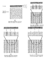
- FIG. 1 illustrates an example of a basic structure of a thin-layer solar cell according to the present disclosure
- FIG. 2 illustrates an alternative example of a basic structure of a thin-layer solar cell according to the present disclosure
- FIG. 3 illustrates an example process for applying electrically conducting paste or electrically insulating paste to a thin-layer solar cell according to the present disclosure
- FIG. 4 illustrates an example of a thin-layer solar cell including a structure of a joint according to the present disclosure
- FIG. 5 illustrates an alternative example of a thin-layer solar cell including a structure of a joint according to the present disclosure
- FIG. 6 illustrates an example process for surface treatment of a thin-layer solar cell (Aspect A) according to the present disclosure
- FIG. 7 illustrates an alternative example process for surface treatment of a thin-layer solar cell (Aspect A) according to the present disclosure.
- FIG. 8 illustrates an alternative example process for surface treatment of a thin-layer solar cell (Aspect B) according to the present disclosure.
- FIG. 9 illustrates an example of a process sequence for Aspect A.
- FIG. 10 illustrates an alternative to the invention-specific connection.
- FIG. 11 illustrates an alternative to the invention-specific structure by additional application of electrically conducting contact fingers.
- the point of departure is a substrate coated with the individual layers necessary for a thin-layer solar cell (see FIG. 1 and FIG. 6 ( a )).
- the layers on the substrate are then surface-treated.
- the layers are subdivided into individual segments.
- Three surface treatments (A, B, C) are necessary per individual segment (see FIG. 6 ( b )).
- surface treatments A and B fully separate layers 3 , 4 and 5 , so that layer 2 becomes visible.
- Surface treatment C fully separates layers 2 , 3 , 4 and 5 , so that the substrate ( 1 ) becomes visible.
- the layers can be divided mechanically with a scriber, for example. What counts here are to find the optimal parameters for removal of the individual layers.
- the power of the scriber, the traversing speed of the scriber, the radius of the scriber tip or the number of scriber passes can be adjusted.
- the parameters for surface treatments A and B are to be chosen so that damage to layer 2 is avoided, but nonetheless complete removal of layers 3 , 4 and 5 is ensured.
- the parameters of surface treatment C are to be so chosen that a complete splitting up of layer 2 is ensured without impairing the function of the substrate ( 1 ).
- the substrate is not to be superficially removed. True, a superficial removal of the substrate is not problematical as long as the stability of the substrate is not affected.
- Trenches A, B and C can be opened up according to the invention while using a laser beam or through the combination of lithography and wet chemical etching or vacuum-based dry etching techniques.
- the distances of the 3 surface treatments of a segment from each other are in essence determined by the positional precision in filling the surface-treated trenches and the guiding of the electrically conducting and electrically insulating polymeric pastes, and should be optimized in regard to minimizing solar-inactive surfaces.
- the generated trenches are to be filled with electrically insulating polymeric paste (trenches A and C) and electrically conducting polymeric paste (trench B).
- a dispenser either with a pressure-loaded cartridge or a dispenser with a spindle valve or a dispenser with a jet valve can be used, with the last-named system ensuring higher throughputs in the context of mass production.
- screen printing technology or technologies related in type can be used.
- the electrically insulating polymeric paste fills trenches A and C (see FIG. 6 ( c )). Trenches A and C are filled so that no electrically insulating polymeric paste gets into trench B. In addition, trenches A and C must be completely filled, with no parts of the trenches remaining unfilled.
- the electrically conducting paste must be applied in trench B and out beyond trench C (see FIG. 6 ( d )).
- the polymeric pastes filled into the trenches must be dried after application in accordance with the instructions of the manufacturer. Depending on the polymer system of the pastes, this can be done in a return air drying oven or under UV irradiation. Thus, an electrical connection is created between the rear contact layer of one segment and the front contact layer of the adjoining segment (see FIG. 6 ( d )).
- the electrically conducting polymeric paste must not extend out far enough over the non-conducting filling of trench C that electrical contact to the transparent front contact layer is possible. How large at the end the surface is, which touches the transparent front contact, depends on the type of the transparent front contact and the conducting polymeric paste. Here an optimization must be carried out in regard to electrical losses and shadowing of active cell surfaces.
- the example is described using FIG. 7 .
- the point of departure is a 15-75- ⁇ m-thick polyimide foil as the substrate ( 1 ).
- This is coated by molybdenum over the entire surface to about 0.2 to 2 ⁇ m thick, as an example, by means of magnetron sputtering.
- This molybdenum layer serves as the back contact layer ( 2 ) of the solar cell.
- other metals or metallic layers could serve as back contact layers.
- the elements copper, indium, gallium and selenium are deposited by means of Kover damping in vacuum.
- other known technologies for depositing the CIGS layer can be used. Among these are sequential deposition, galvanic deposition, printing technologies, or ion-beam-supported deposition.
- a thin (10 to 100 nm) cadmium sulfide layer is then applied by the wet chemical method.
- the CdS layer can also be furnished by a vacuum-based technology. It is also within the invention to use possible Cd-free buffer layers.
- On the buffer layer follows a thin (10 to 100 nm) intrinsic zinc oxide layer (i-ZnO), applied by means of RF sputtering ( 4 ).
- i-ZnO intrinsic zinc oxide layer
- Al:ZnO zinc oxide layer doped with aluminum
- the i-ZnO layer and the Al:ZnO layer are, for simplification, shown as the front contact layer ( 5 ).
- the Al:ZnO layer can also consist of ITO.
- the individual layers can also be furnished in an batch process and in a continuous process (for example roll-to-roll).
- the polyimide band provided with the above-named coatings is dressed to a size of 5 cm ⁇ 5 cm and is now the point of departure for the surface treatment of the layers and the series connection to follow (see FIG. 7 ( a )).
- the 5 cm ⁇ 5 cm coated polyimide foil is equipped with 18 parallel surface treatments as shown in FIG. 7 ( b ), with every three surface treatments arranged in groups.
- the sequence of the surface treatment lines (see FIG. 7 ( b )) is ABCABC . . . etc.
- the surface treatment A is the start. This is carried out for example mechanically using a scriber. The scriber itself is secured to an x-y-z table and is guided with computer support.
- the processing parameters of the scriber are so adapted that layers 3 , 4 and 5 are completely removed along the surface-treatment line without thereby destroying layer 2 .
- the length of the surface-treatment line is 5 cm (length of the coated substrate).
- the width of the line is in essence determined by the radius of the scriber tip. In the example, the line width was 70 ⁇ m; other typical line widths were about 10 to 100 ⁇ m.
- the displacement can so be 50-500 ⁇ m. Since surface treatments A and B are identical, surface treatment B is done according to the scheme of surface treatment A. After surface treatment B is concluded, surface treatment C occurs. This is done parallel to surface treatment B, displaced by 300 ⁇ m. But the displacement can also be 50-500 ⁇ m.
- surface treatment C is carried out by means of a scriber. Varying from surface treatments A and B, the parameters were so adapted that in addition to layers 3 , 4 and 5 , layer 2 was also separated.
- surface-treatment step C If surface-treatment step C is complete, then the surface-treatment steps A, B and C just described are repeated, with this next grouping of surface treatments being displaced parallel to the first group by about 7 mm, for example.
- the third surface-treatment group is then displaced relative to the second group by 7 mm and so on.
- 6 groups, each with 3 surface-treatment lines are placed (see FIG. 7 ( b )). It should be mentioned that the interval between surface-treatment groups can be between 3 and 15 mm, and depends, among other things, on the electrical properties of the front contact.
- first all of the surface-treatment steps for the trenches A can be carried out on the 5-cm substrate, and thereafter the surface-treatment steps B and C, or in any other sequence desired.
- First trenches A and C are filled with an electrically insulating polymeric paste with the aid of a computer-controlled dispenser on an x-y-z table (see FIG. 7 ( c )). They are filled so that no electrically insulating paste runs into trench B and closes it.
- trenches A and C must be filled with electrically insulating paste with no gaps. This is of especially decisive importance for trench C, because it then is covered by an electrically conducting paste, which for its part then can penetrate into it if trench C is not completely insulated, and can thus lead to a short circuit of two segments. Electrically insulated polymeric pastes can be obtained commercially from various manufacturers.
- the line thickness of the applied paste is dependent on the flow characteristics of the paste. Also, the line thickness can be influenced by the parameters of the dispenser (pressure applied to the cartridge; application rate; diameter of the outlet opening of the cartridge, etc.). Typical line widths are in a range from 1500 to 300 ⁇ m.
- the trenches are to be filled over the entire trench length (in this case 5 cm). After all the trenches A and C have been filled with electrically insulating paste, the paste must be hardened according to manufacturer specifications by means of a return-air drying oven or by IR or UV radiation.
- all the trenches B can be filled with electrically conducting paste with the aid of a dispenser (see FIG. 7 ( d )).
- the line thickness of the applied paste is dependent on the flow characteristics of the paste.
- the line thickness can be influenced by the parameters of the dispenser (pressure applied to the cartridge; application rate; diameter of the outlet opening of the cartridge, etc.).
- the electrically conducting paste must be applied so that trench B is completely filled, without running out over the insulated filling of trench A, since otherwise the segment will short-circuit. Additionally, the electrically conducting paste in every case must be directed over the insulated filling of trench C, thus guaranteeing contact with the front contact layer of the following segment.
- Typical line widths of the electrically conducting fillings are 400 to 700 ⁇ m, and among other things depend on the interval of trenches B and C.
- Electrically insulated polymeric pastes can be obtained commercially from various manufacturers. After all the trenches B have been filled with electrically insulating paste, the paste must be hardened according to manufacturer specifications in a return-air drying oven or with IR or UV radiation.
- Varying from the process sequence in Aspect A first in the layer package (see FIG. 8 ( a )) only surface treatments B and C are carried out (see FIG. 8 ( b )). Then trench C is filled with electrically insulating paste (see FIG. 8 ( c )). The insulating paste is dried in accordance with manufacturer's specifications. Then, the electrically conducting polymeric paste in trenches B and over the filling of trench C outward is filled with an electrically conducting polymeric paste (see FIG. 8 ( d )). Then the surface treatment A is carried out (see FIG. 8 ( e )). For minimizing solar-inactive surfaces, it is advantageous to set the surface treatment A as much as possible on the edge of the filling of electrically conducting polymeric paste.
- the surface treatment A can be adapted to the molding out of the edges of the filling of electrically conducting paste. Both of the last-named possibilities can minimize the size of inactive surfaces and thus increase the effectiveness of the solar cells. Additionally, one processing step (filling trench A with electrically insulating paste) can be saved, thus lowering production costs.
- the polyimide band provided with the above-named coatings is trimmed for example to a size of 5 cm ⁇ 5 cm and is now the point of departure for surface treatment of the layers and the series connection that follows.
- the 5 cm ⁇ 5 cm coated polyimide foil is, as shown in FIG. 9 ( b ), first provided with 12 parallel surface treatments, with every two surface treatments arranged in groups.
- the sequence of the surface-treatment lines (see FIG. 9 ( b )) is BCBC . . . etc.
- the surface treatment B is the start. This is carried out for example mechanically using a scriber.
- the scriber itself is secured to an x-y-z table and is guided with computer support.
- the processing parameters of the scriber are so adapted that layers 3 , 4 and 5 are completely removed along the surface-treatment line without thereby destroying layer 2 .
- the length of the surface-treatment line is 5 cm (length of the coated substrate).
- the width of the line is in essence determined by the radius of the scriber tip. In the example, the line width was 70 ⁇ m; other typical line widths are about 10 to 100 ⁇ m.
- surface treatment C occurs. This lies parallel to surface treatment B, displaced by 300 ⁇ m. However, the displacement can be 50-500 ⁇ m.
- Surface treatment C is carried out for example by means of a scriber. Varying from surface treatment B, the parameters were so adapted that in addition to layers 3 , 4 and 5 , layer 2 was also separated.
- trenches C are filled with an electrically insulating polymeric paste with the aid of a computer-controlled dispenser on an x-y-z table (see FIG. 9 ( c )). They are to be filled so that no electrically insulating paste runs into trench B and closes it.
- trench C must be filled with electrically insulating paste with no gaps. This is of especial decisive importance for trench C, because it then is covered by an electrically conducting paste, which for its part then can penetrate into it if trench C is not completely insulated, and can thus lead to a short circuit of two segments. Electrically insulated polymeric pastes can be obtained commercially from various manufacturers. The line thickness of the applied paste is dependent on the flow characteristics of the paste.
- the line thickness can be influenced by the parameters of the dispenser (pressure applied to the cartridge; application rate; diameter of the outlet opening of the cartridge, etc.). Typical line widths are in a range from 1500 to 300 ⁇ m.
- the trenches are to be filled over the entire trench length (in this case 5 cm). After the trenches C have been filled with electrically insulating paste, the paste must be hardened according to manufacturer specifications by means of a return-air drying oven or by IR or UV radiation.
- the line thickness of the applied paste is dependent on the flow characteristics of the paste. Also, the line thickness can be influenced by the parameters of the dispenser (pressure applied to the cartridge; application rate; diameter of the outlet opening of the cartridge, etc.).
- the electrically conducting paste must in every case must be directed over the insulated filling of trench C, thus guaranteeing contact with the front contact layer of the following segment. Typical line widths of the electrically conducting fillings are 400 to 700 ⁇ m, and among other things depend on the interval of trenches B and C. Electrically insulated polymeric pastes can be obtained commercially from various manufacturers. After all the trenches B have been filled with electrically insulating paste, the paste is hardened according to manufacturer specifications in a return-air drying oven or with IR or UV radiation.
- surface treatment A can take place.
- Surface treatment A is set on the left ( FIG. 9 ( e )) by the filling of trench B.
- Surface treatment A is carried out for example mechanically with the aid of a scriber.
- Surface treatment A should for one thing extend as tightly as possible to the filling of trench B.
- All of the surface treatments can also be done using lasers or by photolithography in combination with an etching technology (wet chemical or vacuum-based dry etching method). A combination of all of those methods named is also possible.
- the substrate can be electrically insulating or electrically conducting.
- an electrically insulating layer In the case of an electrically conducting substrate, such as a metal foil, an electrically insulating layer must be placed on this substrate, i.e., between the substrate ( 1 ) and the back contact layer ( 2 ), to avoid a short circuit of the individual segments via their back contact layers, which would lead to a considerable impairment of the function of the later connection.
- the parameters of surface treatment C can here be chosen so that the electrically insulating layer can be removed or remains on the substrate; what is decisive is that the back contact layer is completely separated.
- Filling of trenches A and C with electrically insulating polymeric paste can also be replaced by coating with an electrically insulating material such as SiOx, by means of vacuum separation or galvanic separation.
- Filling of trench B with electrically conducting polymeric paste can also be replaced by an electrically conducting material like silver by means of vacuum separation or galvanic separation.
- trenches A, B and C it is also possible, for filling trenches A, B and C, to combine the methods for applying a polymeric paste with the methods of vacuum separation and galvanic separation.
- the surface treatment steps A, B and C can in principle be so tight that between the surface-treated trenches that no more layer packages are present (see FIG. 10 ( i )).
- the surface-treatment step for the trench A and the trench B are replaced by a single surface-treatment step.
- this also has an advantage in that the inactive surface of the solar cell is reduced, and thus the efficiency of the solar cell is increased.
- the trenches can also be filled with electrically insulating and electrically conducting paste by means of serigraphy, screen printing, ink-jet or spray methods (using masks). Generally a combination of the individual methods named is also conceivable.
- paste systems based on silicon or acrylate can also be used.
- these can for example be further applied in the form of individual contact fingers onto the active solar cell surface, thus supporting the conductivity of the front contact layer, through which the intervals of the individual segments from each other can be increased, and thus after an optimization of serial resistance losses and shadowings of solar-active surfaces, a maximum of solar-active surface can be achieved (see FIG. 11 ).
- the invention-specific method can be applied to every type of thin-layer solar cell on a flexible substrate.
- the following types serve as examples:
Landscapes
- Photovoltaic Devices (AREA)
Applications Claiming Priority (4)
| Application Number | Priority Date | Filing Date | Title |
|---|---|---|---|
| DE102009041905 | 2009-09-20 | ||
| DE102009041905A DE102009041905B4 (de) | 2009-09-20 | 2009-09-20 | Verfahren zur seriellen Verschaltung von Dünnschichtsolarzellen |
| DE102009041905.5 | 2009-09-20 | ||
| PCT/EP2010/005718 WO2011032717A2 (de) | 2009-09-20 | 2010-09-17 | Serielle verschaltung von dünnschichtsolarzellen |
Publications (2)
| Publication Number | Publication Date |
|---|---|
| US20120276681A1 US20120276681A1 (en) | 2012-11-01 |
| US8778723B2 true US8778723B2 (en) | 2014-07-15 |
Family
ID=43759082
Family Applications (1)
| Application Number | Title | Priority Date | Filing Date |
|---|---|---|---|
| US13/496,779 Active 2031-01-26 US8778723B2 (en) | 2009-09-20 | 2010-09-17 | Serial connection of thin-layer solar cells |
Country Status (6)
| Country | Link |
|---|---|
| US (1) | US8778723B2 (de) |
| EP (1) | EP2478559A2 (de) |
| CN (1) | CN102598268A (de) |
| BR (1) | BR112012006222A2 (de) |
| DE (1) | DE102009041905B4 (de) |
| WO (1) | WO2011032717A2 (de) |
Cited By (2)
| Publication number | Priority date | Publication date | Assignee | Title |
|---|---|---|---|---|
| USD720313S1 (en) * | 2014-06-16 | 2014-12-30 | Emcore Solar Power, Inc. | Semiconductor wafer with dicing positions for solar cell fabrication |
| US20150068578A1 (en) * | 2012-04-02 | 2015-03-12 | Robert Bosch Gmbh | method for manufacturing thin-film solar modules, and thin-film solar modules which are obtainable according to this method |
Families Citing this family (11)
| Publication number | Priority date | Publication date | Assignee | Title |
|---|---|---|---|---|
| KR101166456B1 (ko) * | 2011-05-23 | 2012-07-19 | 김병국 | 태양전지 및 그 제조방법 |
| DE102012205978A1 (de) * | 2012-04-12 | 2013-10-17 | Robert Bosch Gmbh | Photovoltaische Dünnschichtsolarmodule sowie Verfahren zur Herstellung solcher Dünnschichtsolarmodule |
| CN103474485B (zh) * | 2013-09-17 | 2016-08-17 | 北京汉能创昱科技有限公司 | 一种柔性薄膜太阳能电池及其制备方法 |
| US20150303326A1 (en) * | 2014-04-18 | 2015-10-22 | Tsmc Solar Ltd. | Interconnect for a thin film photovoltaic solar cell, and method of making the same |
| NL2014041B1 (en) * | 2014-12-23 | 2016-10-12 | Stichting Energieonderzoek Centrum Nederland | Method for manufacturing a thin film solar cell arrangement and such a thin film solar cell arrangement. |
| FR3060854B1 (fr) * | 2016-12-16 | 2021-05-14 | Armor | Procede de fabrication d'un module photovoltaique et module photovoltaique ainsi obtenu |
| FR3082356B1 (fr) | 2018-06-11 | 2020-06-19 | Armor | Procede de fabrication d'un module photovoltaique et module photovoltaique ainsi obtenu |
| DE102019117215B4 (de) * | 2019-06-26 | 2022-10-06 | Deutsches Zentrum für Luft- und Raumfahrt e.V. | Raumfahrzeugmembraneinheit |
| EP3945589A1 (de) | 2020-07-27 | 2022-02-02 | Armor | Verfahren zur herstellung eines halbleitermoduls und dadurch erhaltenes halbleitermodul |
| EP4195296B1 (de) * | 2020-12-28 | 2026-02-11 | Suzhou Institute of Nano-tech and Nano-bionics (SINANO) Chinese Academy of Sciences | Flexible fotoelektrische komponentenanordnung und herstellungsverfahren dafür |
| CN115172500B (zh) * | 2022-07-12 | 2023-08-15 | 中国电子科技集团公司第十八研究所 | 一种激光电池组件 |
Citations (9)
| Publication number | Priority date | Publication date | Assignee | Title |
|---|---|---|---|---|
| US5593901A (en) | 1989-09-08 | 1997-01-14 | Amoco/Enron Solar | Monolithic series and parallel connected photovoltaic module |
| US6541693B2 (en) * | 1998-01-21 | 2003-04-01 | Canon Kabushiki Kaisha | Solar cell module and process for its production, and solar cell module installing method and solar electricity generation system |
| JP2004260013A (ja) | 2003-02-26 | 2004-09-16 | Kyocera Corp | 光電変換装置及びその製造方法 |
| EP1727211A1 (de) | 2005-05-27 | 2006-11-29 | Sharp Kabushiki Kaisha | Dünnschichtsolarzelle und ihr Herstellungsverfahren |
| EP1918993A1 (de) | 2006-11-02 | 2008-05-07 | Manz Automation AG | Verfahren zum Strukturieren von Solarmodulen und Strukturierungsvorrichtung |
| WO2008157807A2 (en) | 2007-06-20 | 2008-12-24 | Ascent Solar Technologies, Inc. | Array of monolithically integrated thin film photovoltaic cells and associated methods |
| WO2009067526A2 (en) | 2007-11-19 | 2009-05-28 | Sheats James R | High-efficiency, high current solar cell and solar module |
| US20100015752A1 (en) * | 2008-07-16 | 2010-01-21 | Konarka Technologies, Inc. | Methods of Preparing Photovoltaic Modules |
| US8319097B2 (en) * | 1999-03-30 | 2012-11-27 | Daniel Luch | Substrate and collector grid structures for integrated series connected photovoltaic arrays and process of manufacture of such arrays |
Family Cites Families (10)
| Publication number | Priority date | Publication date | Assignee | Title |
|---|---|---|---|---|
| JP2000058886A (ja) * | 1998-08-14 | 2000-02-25 | Mitsubishi Heavy Ind Ltd | 太陽電池モジュール及びその製造方法 |
| US6690041B2 (en) * | 2002-05-14 | 2004-02-10 | Global Solar Energy, Inc. | Monolithically integrated diodes in thin-film photovoltaic devices |
| DE10333960A1 (de) * | 2003-07-25 | 2005-02-10 | Robert Bosch Gmbh | Vorrichtung zur kapazitiven Druckmessung sowie Vefahren zur Herstellung einer kapazitiven Druckmessvorrichtung |
| JP2005101384A (ja) * | 2003-09-26 | 2005-04-14 | Sanyo Electric Co Ltd | 光起電力装置及びその製造方法 |
| US20070079866A1 (en) * | 2005-10-07 | 2007-04-12 | Applied Materials, Inc. | System and method for making an improved thin film solar cell interconnect |
| JP2007123532A (ja) * | 2005-10-27 | 2007-05-17 | Honda Motor Co Ltd | 太陽電池 |
| TW200849621A (en) * | 2006-12-21 | 2008-12-16 | Helianthos Bv | Method for making solar sub-cells from a solar cell |
| JP4425296B2 (ja) * | 2007-07-09 | 2010-03-03 | 三洋電機株式会社 | 光起電力装置 |
| US20090084425A1 (en) * | 2007-09-28 | 2009-04-02 | Erel Milshtein | Scribing Methods for Photovoltaic Modules Including a Mechanical Scribe |
| KR101119235B1 (ko) * | 2008-07-04 | 2012-03-21 | 가부시키가이샤 아루박 | 태양 전지 셀의 제조 방법 및 태양 전지 셀 |
-
2009
- 2009-09-20 DE DE102009041905A patent/DE102009041905B4/de not_active Expired - Fee Related
-
2010
- 2010-09-17 EP EP10760919.0A patent/EP2478559A2/de not_active Withdrawn
- 2010-09-17 WO PCT/EP2010/005718 patent/WO2011032717A2/de not_active Ceased
- 2010-09-17 BR BR112012006222A patent/BR112012006222A2/pt not_active Application Discontinuation
- 2010-09-17 CN CN2010800474614A patent/CN102598268A/zh active Pending
- 2010-09-17 US US13/496,779 patent/US8778723B2/en active Active
Patent Citations (10)
| Publication number | Priority date | Publication date | Assignee | Title |
|---|---|---|---|---|
| US5593901A (en) | 1989-09-08 | 1997-01-14 | Amoco/Enron Solar | Monolithic series and parallel connected photovoltaic module |
| US6541693B2 (en) * | 1998-01-21 | 2003-04-01 | Canon Kabushiki Kaisha | Solar cell module and process for its production, and solar cell module installing method and solar electricity generation system |
| US8319097B2 (en) * | 1999-03-30 | 2012-11-27 | Daniel Luch | Substrate and collector grid structures for integrated series connected photovoltaic arrays and process of manufacture of such arrays |
| JP2004260013A (ja) | 2003-02-26 | 2004-09-16 | Kyocera Corp | 光電変換装置及びその製造方法 |
| EP1727211A1 (de) | 2005-05-27 | 2006-11-29 | Sharp Kabushiki Kaisha | Dünnschichtsolarzelle und ihr Herstellungsverfahren |
| EP1918993A1 (de) | 2006-11-02 | 2008-05-07 | Manz Automation AG | Verfahren zum Strukturieren von Solarmodulen und Strukturierungsvorrichtung |
| US20090000108A1 (en) | 2006-11-02 | 2009-01-01 | Dieter Manz | Method for structuring solar modules and structuring device |
| WO2008157807A2 (en) | 2007-06-20 | 2008-12-24 | Ascent Solar Technologies, Inc. | Array of monolithically integrated thin film photovoltaic cells and associated methods |
| WO2009067526A2 (en) | 2007-11-19 | 2009-05-28 | Sheats James R | High-efficiency, high current solar cell and solar module |
| US20100015752A1 (en) * | 2008-07-16 | 2010-01-21 | Konarka Technologies, Inc. | Methods of Preparing Photovoltaic Modules |
Non-Patent Citations (1)
| Title |
|---|
| International Search Report (in German with English translation) for PCT/EP2010/005718, mailed Dec. 19, 2011; ISA/EP. |
Cited By (2)
| Publication number | Priority date | Publication date | Assignee | Title |
|---|---|---|---|---|
| US20150068578A1 (en) * | 2012-04-02 | 2015-03-12 | Robert Bosch Gmbh | method for manufacturing thin-film solar modules, and thin-film solar modules which are obtainable according to this method |
| USD720313S1 (en) * | 2014-06-16 | 2014-12-30 | Emcore Solar Power, Inc. | Semiconductor wafer with dicing positions for solar cell fabrication |
Also Published As
| Publication number | Publication date |
|---|---|
| WO2011032717A2 (de) | 2011-03-24 |
| BR112012006222A2 (pt) | 2016-05-31 |
| EP2478559A2 (de) | 2012-07-25 |
| WO2011032717A3 (de) | 2012-03-08 |
| US20120276681A1 (en) | 2012-11-01 |
| DE102009041905A1 (de) | 2011-04-28 |
| DE102009041905B4 (de) | 2013-08-22 |
| CN102598268A (zh) | 2012-07-18 |
Similar Documents
| Publication | Publication Date | Title |
|---|---|---|
| US8778723B2 (en) | Serial connection of thin-layer solar cells | |
| US7122398B1 (en) | Manufacturing of optoelectronic devices | |
| CN101743643B (zh) | 薄膜太阳能电池模块及其制造方法 | |
| US5268037A (en) | Monolithic, parallel connected photovoltaic array and method for its manufacture | |
| TWI433340B (zh) | 半導體元件以及增加半導體元件有效運作面積的方法 | |
| EP2416377B1 (de) | Solarzelle und verfahren zu ihrer herstellung | |
| CN103563082B (zh) | 光伏器件及其制造方法 | |
| CN102203948A (zh) | 薄膜太阳能电池和光伏串组件 | |
| JP2009529805A (ja) | 絶縁ビアを備えた高効率太陽電池 | |
| US20170077320A1 (en) | Anti-corrosion protection of photovoltaic structures | |
| US8779282B2 (en) | Solar cell apparatus and method for manufacturing the same | |
| US20180151766A1 (en) | Anti-corrosion protection in photovoltaic structures | |
| US20070089780A1 (en) | Serial circuit of solar cells with integrated semiconductor bodies, corresponding method for production and module with serial connection | |
| US8283199B2 (en) | Solar cell patterning and metallization | |
| US8114702B2 (en) | Method of manufacturing a monolithic thin-film photovoltaic device with enhanced output voltage | |
| US11569400B2 (en) | Circuit configuration for power generation comprising series-connected solar cells having bypass diodes | |
| KR20110001793A (ko) | 태양전지 및 이의 제조방법 | |
| US12290879B2 (en) | Method for creating shunt free translucent flexible thin-film photovoltaic module | |
| US20180102452A1 (en) | Corrosion resistant photovoltaic modules | |
| WO2017008120A1 (en) | A method for forming a contacting structure to a back contact solar cell | |
| US20120024340A1 (en) | Solar Cells With Localized Silicon/Metal Contact For Hot Spot Mitigation and Methods of Manufacture | |
| US8648250B2 (en) | Multi-stack semiconductor device | |
| WO2010118906A2 (en) | Thin-film solar cell module | |
| JP2013149699A (ja) | 集積化太陽電池の製造方法 | |
| US9070810B2 (en) | Multiple solar cell and method for manufacturing the same |
Legal Events
| Date | Code | Title | Description |
|---|---|---|---|
| AS | Assignment |
Owner name: SOLARION AG PHOTOVOLTAIK, GERMANY Free format text: ASSIGNMENT OF ASSIGNORS INTEREST;ASSIGNORS:OTTE, KARSTEN;BRAUN, ALEXANDER;RAGNOW, STEFFEN;AND OTHERS;SIGNING DATES FROM 20120330 TO 20120413;REEL/FRAME:028101/0795 |
|
| STCF | Information on status: patent grant |
Free format text: PATENTED CASE |
|
| AS | Assignment |
Owner name: SOLARION AG, GERMANY Free format text: NUNC PRO TUNC ASSIGNMENT;ASSIGNORS:OTTE, KARSTEN;BRAUN, ALEXANDER;RAGNOW, STEFFEN;AND OTHERS;SIGNING DATES FROM 20140716 TO 20140807;REEL/FRAME:033514/0277 |
|
| CC | Certificate of correction | ||
| AS | Assignment |
Owner name: OC3 AG, GERMANY Free format text: ASSIGNMENT OF ASSIGNORS INTEREST;ASSIGNOR:SOLARION AG;REEL/FRAME:038654/0476 Effective date: 20160324 |
|
| FEPP | Fee payment procedure |
Free format text: MAINTENANCE FEE REMINDER MAILED (ORIGINAL EVENT CODE: REM.) |
|
| FEPP | Fee payment procedure |
Free format text: SURCHARGE FOR LATE PAYMENT, SMALL ENTITY (ORIGINAL EVENT CODE: M2554) |
|
| MAFP | Maintenance fee payment |
Free format text: PAYMENT OF MAINTENANCE FEE, 4TH YR, SMALL ENTITY (ORIGINAL EVENT CODE: M2551) Year of fee payment: 4 |
|
| FEPP | Fee payment procedure |
Free format text: MAINTENANCE FEE REMINDER MAILED (ORIGINAL EVENT CODE: REM.); ENTITY STATUS OF PATENT OWNER: SMALL ENTITY |
|
| FEPP | Fee payment procedure |
Free format text: 7.5 YR SURCHARGE - LATE PMT W/IN 6 MO, SMALL ENTITY (ORIGINAL EVENT CODE: M2555); ENTITY STATUS OF PATENT OWNER: SMALL ENTITY |
|
| MAFP | Maintenance fee payment |
Free format text: PAYMENT OF MAINTENANCE FEE, 8TH YR, SMALL ENTITY (ORIGINAL EVENT CODE: M2552); ENTITY STATUS OF PATENT OWNER: SMALL ENTITY Year of fee payment: 8 |
|
| MAFP | Maintenance fee payment |
Free format text: PAYMENT OF MAINTENANCE FEE, 12TH YR, SMALL ENTITY (ORIGINAL EVENT CODE: M2553); ENTITY STATUS OF PATENT OWNER: SMALL ENTITY Year of fee payment: 12 |