US8822335B2 - Semiconductor device with air gap and method for fabricating the same - Google Patents
Semiconductor device with air gap and method for fabricating the same Download PDFInfo
- Publication number
- US8822335B2 US8822335B2 US13/843,794 US201313843794A US8822335B2 US 8822335 B2 US8822335 B2 US 8822335B2 US 201313843794 A US201313843794 A US 201313843794A US 8822335 B2 US8822335 B2 US 8822335B2
- Authority
- US
- United States
- Prior art keywords
- layer
- forming
- plug
- storage node
- over
- Prior art date
- Legal status (The legal status is an assumption and is not a legal conclusion. Google has not performed a legal analysis and makes no representation as to the accuracy of the status listed.)
- Expired - Fee Related
Links
Images



Classifications
-
- H—ELECTRICITY
- H10—SEMICONDUCTOR DEVICES; ELECTRIC SOLID-STATE DEVICES NOT OTHERWISE PROVIDED FOR
- H10W—GENERIC PACKAGES, INTERCONNECTIONS, CONNECTORS OR OTHER CONSTRUCTIONAL DETAILS OF DEVICES COVERED BY CLASS H10
- H10W10/00—Isolation regions in semiconductor bodies between components of integrated devices
- H10W10/01—Manufacture or treatment
- H10W10/021—Manufacture or treatment of air gaps
-
- H—ELECTRICITY
- H10—SEMICONDUCTOR DEVICES; ELECTRIC SOLID-STATE DEVICES NOT OTHERWISE PROVIDED FOR
- H10W—GENERIC PACKAGES, INTERCONNECTIONS, CONNECTORS OR OTHER CONSTRUCTIONAL DETAILS OF DEVICES COVERED BY CLASS H10
- H10W20/00—Interconnections in chips, wafers or substrates
- H10W20/01—Manufacture or treatment
- H10W20/031—Manufacture or treatment of conductive parts of the interconnections
- H10W20/069—Manufacture or treatment of conductive parts of the interconnections by forming self-aligned vias or self-aligned contact plugs
-
- H—ELECTRICITY
- H10—SEMICONDUCTOR DEVICES; ELECTRIC SOLID-STATE DEVICES NOT OTHERWISE PROVIDED FOR
- H10W—GENERIC PACKAGES, INTERCONNECTIONS, CONNECTORS OR OTHER CONSTRUCTIONAL DETAILS OF DEVICES COVERED BY CLASS H10
- H10W20/00—Interconnections in chips, wafers or substrates
- H10W20/01—Manufacture or treatment
- H10W20/071—Manufacture or treatment of dielectric parts thereof
- H10W20/072—Manufacture or treatment of dielectric parts thereof of dielectric parts comprising air gaps
-
- H—ELECTRICITY
- H10—SEMICONDUCTOR DEVICES; ELECTRIC SOLID-STATE DEVICES NOT OTHERWISE PROVIDED FOR
- H10W—GENERIC PACKAGES, INTERCONNECTIONS, CONNECTORS OR OTHER CONSTRUCTIONAL DETAILS OF DEVICES COVERED BY CLASS H10
- H10W20/00—Interconnections in chips, wafers or substrates
- H10W20/01—Manufacture or treatment
- H10W20/071—Manufacture or treatment of dielectric parts thereof
- H10W20/074—Manufacture or treatment of dielectric parts thereof of dielectric parts comprising thin functional dielectric layers, e.g. dielectric etch-stop, barrier, capping or liner layers
- H10W20/076—Manufacture or treatment of dielectric parts thereof of dielectric parts comprising thin functional dielectric layers, e.g. dielectric etch-stop, barrier, capping or liner layers in via holes or trenches
-
- H—ELECTRICITY
- H10—SEMICONDUCTOR DEVICES; ELECTRIC SOLID-STATE DEVICES NOT OTHERWISE PROVIDED FOR
- H10W—GENERIC PACKAGES, INTERCONNECTIONS, CONNECTORS OR OTHER CONSTRUCTIONAL DETAILS OF DEVICES COVERED BY CLASS H10
- H10W20/00—Interconnections in chips, wafers or substrates
- H10W20/40—Interconnections external to wafers or substrates, e.g. back-end-of-line [BEOL] metallisations or vias connecting to gate electrodes
- H10W20/45—Interconnections external to wafers or substrates, e.g. back-end-of-line [BEOL] metallisations or vias connecting to gate electrodes characterised by their insulating parts
- H10W20/46—Interconnections external to wafers or substrates, e.g. back-end-of-line [BEOL] metallisations or vias connecting to gate electrodes characterised by their insulating parts comprising air gaps
-
- H—ELECTRICITY
- H10—SEMICONDUCTOR DEVICES; ELECTRIC SOLID-STATE DEVICES NOT OTHERWISE PROVIDED FOR
- H10W—GENERIC PACKAGES, INTERCONNECTIONS, CONNECTORS OR OTHER CONSTRUCTIONAL DETAILS OF DEVICES COVERED BY CLASS H10
- H10W20/00—Interconnections in chips, wafers or substrates
- H10W20/01—Manufacture or treatment
- H10W20/031—Manufacture or treatment of conductive parts of the interconnections
- H10W20/032—Manufacture or treatment of conductive parts of the interconnections of conductive barrier, adhesion or liner layers
- H10W20/033—Manufacture or treatment of conductive parts of the interconnections of conductive barrier, adhesion or liner layers in openings in dielectrics
- H10W20/036—Manufacture or treatment of conductive parts of the interconnections of conductive barrier, adhesion or liner layers in openings in dielectrics the barrier, adhesion or liner layers being within a main fill metal
Definitions
- Exemplary embodiments of the present invention relate to a semiconductor device, and more particularly, to a semiconductor device with an air gap and a method for fabricating the same.
- a semiconductor device includes a second conductive structure formed with an insulation layer provided between a plurality of first conductive structures.
- the first conductive structure may include a gate, a bit line, a metal interconnection and the like
- the second conductive structure may include a contact plug, a storage node contact plug, a bit line contact plug, a via and the like.
- an insulation layer used in a semiconductor device may include silicon oxide and silicon nitride.
- the silicon oxide has a dielectric constant of about 4, and the silicon nitride has a dielectric constant of about 7.
- the silicon oxide and the silicon nitride have high dielectric constants, they have a limitation in reducing parasitic capacitance. Recently, materials having relatively low dielectric constants have been developed, but the dielectric constants thereof may be not so low.
- Various exemplary embodiments of the present invention are directed to a semiconductor device that may reduce parasitic capacitance between adjacent conductive structures, and a method for fabricating the same.
- a method for fabricating a semiconductor device includes forming a semiconductor structure having an open portion over a substrate; forming a sacrificial spacer on sidewalls of the open portion; forming a recessed first plug in the open portion; forming an air gap by removing the sacrificial spacer; forming a capping layer to expose a top surface of the recessed first plug and to cap the air gap; forming a protective layer over the capping layer and the recessed first plug; forming an ohmic contact layer over the protective layer; and forming a second plug over the ohmic contact layer.
- a method for fabricating a semiconductor device includes forming a plurality of bit line structures over a substrate; forming a storage node contact hole between the bit line structures; forming a sacrificial spacer on sidewalls of the storage node contact hole; forming a recessed first storage node contact plug in the storage node contact hole; forming an air gap by removing the sacrificial spacer; forming oxide by oxidizing the surface of the recessed first storage node contact plug; etching the oxide to expose a top surface of the recessed first storage node contact plug, and forming a capping layer to cap the air gap; forming a protective layer over the capping layer and the first storage node contact plug; forming an ohmic contact layer over the protective layer; and forming a second storage node contact plug over the ohmic contact layer.
- a method for fabricating a semiconductor device includes forming a semiconductor structure having an open portion exposing a portion of a substrate; forming a sacrificial spacer on sidewalls of the semiconductor structure; forming a recessed first plug in the open portion; forming an air gap by removing the sacrificial spacer; forming a capping layer to cap the air gap; forming a protective layer over the capping layer and the recessed first plug; and forming a second plug over the protective layer.
- a semiconductor device in still another exemplary embodiment of the present invention, includes a plurality of bit line structures formed over a substrate; a storage node contact hole formed to expose sidewalls of the bit line structures; a recessed first storage contact plug formed in the storage node contact hole; an air gap formed between the sidewalls of the bit line structures and the recessed first storage node contact plug; a capping layer capping the air gap; a protective layer formed over the capping layer and the recessed first storage node contact plug; an ohmic contact layer formed over the protective layer; and a second storage node contact plug formed over the ohmic contact layer.
- the capping layer may comprise oxide of the recessed first storage node contact plug.
- the ohmic contact layer may comprise metal silicide, and the protective layer comprises polysilicon.
- the recessed first storage node contact plug may comprise polysilicon, and the second storage node contact plug comprises tungsten.
- a semiconductor device in still another exemplary embodiment of the present invention, includes a semiconductor structure formed over a substrate and having an open portion; a silicon plug formed in the open portion; an air gap formed between the silicon plug and sidewalls of the semiconductor structure; a capping layer exposing a top surface of the silicon plug and capping the air gap; a protective layer including a silicon layer, formed over the capping layer and the silicon plug; an ohmic contact layer including metal silicide, formed over the protective layer; and a metal plug formed over the ohmic contact layer.
- the capping layer may comprise silicon oxide obtained by oxidizing the silicon plug.
- the ohmic contact layer comprises cobalt silicide.
- FIG. 1 is a cross sectional view illustrating a portion of a semiconductor device in accordance with an embodiment of the present invention.
- FIGS. 2A to 2O are cross sectional views illustrating a method for fabricating the semiconductor device in accordance with an embodiment of the present invention.
- FIGS. 3A and 3B illustrate a first comparative embodiment for an embodiment of the present invention.
- FIGS. 4A to 4C illustrate a second comparative embodiment or an embodiment of the present invention.
- FIG. 5A is an arrangement diagram illustrating memory cells of DRAM.
- FIG. 5B is a cross-sectional view of the DRAM taken along line A-A′ of FIG. 5A .
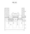
- FIG. 5C is a cross sectional view of the DRAM taken along line B-B′ of FIG. 5A .
- FIG. 6 is a schematic diagram of a memory card.
- FIG. 7 is a block diagram illustrating an electronic system.
- first layer is referred to as being “on” a second layer or “on” a substrate, it not only refers to a case where the first layer is formed directly on the second layer or the substrate but also a case where a third layer exists between the first layer and the second layer or the substrate.
- FIG. 1 is cross sectional view illustrating a portion of a semiconductor device in accordance with an embodiment of the present invention.
- the semiconductor structure may include a conductive structure.
- the conductive structure may include a first conductive structure 104 and a second conductive structure 110 . Between the first and second conductive 104 and 110 , an air gap 111 may be formed.
- a capping layer 112 may be formed over the air gap 111 .
- the first conductive structure 104 may include a first conductive layer 102 .
- the first conductive structure 104 may have a stacked structure of the first conductive layer 102 and a hard mask layer 103 .
- the first conductive layer 102 may include a silicon-containing layer or a metal-containing layer.
- the first conductive layer 102 may be formed by stacking a silicon-containing layer and a metal-containing layer.
- the first conductive layer 102 may include polysilicon, metal, metal nitride, metal silicide or the like.
- the first conductive layer 102 may be formed by stacking polysilicon and metal.
- the metal may include tungsten.
- the hard mask layer 103 may include an insulator.
- the hard mask layer 103 may include oxide or nitride.
- first and second conductive structures 104 and 110 may have a line shape extended in any one direction.
- the other of the first and second conductive structures 104 and 110 may have a plug shape.
- the first conductive structure 104 may include a line-shaped structure
- the second conductive structure 110 may include a plug-shaped structure.
- the first conductive structures 104 may be regularly arranged at even intervals from each other over the substrate 101 .
- the second conductive structure 110 may be formed in an open portion formed between the first conductive structures 104 .
- the open portion may include a contact hole and the like.
- the second conductive structure 110 may include a recessed second conductive layer 106 between the first conductive structures 104 .
- the second conductive structure 110 may have a stacked structure including the second conductive layer 106 , a protective layer 107 , an ohmic contact layer 108 , and a third conductive layer 109 .
- the second conductive layer 106 and the protective layer 107 may include a silicon-containing layer.
- the second conductive layer 106 and the protective layer 107 may include polysilicon.
- the ohmic contact layer 108 and the third conductive layer 109 may include a metal-containing layer.
- the ohmic contact layer 108 may include metal silicide such as cobalt silicide.
- the third conductive layer 109 may include metal, metal silicide, metal nitride or the like.
- the third conductive layer 109 may have a stacked structure of a barrier layer and a metal layer.
- the third conductive layer 109 may be formed by stacking titanium nitride and tungsten.
- the capping layer 112 may be formed in such a shape as to cap the air gap 111 .
- the capping layer 112 may include oxide of the second conductive layer 106 .
- the capping layer 112 may include plasma oxide of the second conductive layer 106 .
- the capping layer 112 may include silicon oxide.
- a spacer 105 may be formed over both sidewalls of the first conductive structure 104 .
- the spacer 105 may include an insulator.
- the spacer 105 may include oxide or nitride.
- the spacer 105 and the air gap 111 may serve to insulate the first and second conductive structures 104 and 110 from each other.
- any one of the first and second conductive structures 104 and 110 may include a gate and a bit line.
- the other of the first and second conductive structures 104 and 110 may include a contact plug.
- the contact plug may include a storage node contact plug, a landing plug and the like.
- the first conductive layer 102 of the first conductive structure 104 may include a bit line
- the second conductive structure 110 may include a storage node contact plug. Therefore, the air gap 111 may be formed between the bit line and the storage node contact plug.
- the second conductive layer 106 may become a first plug
- the third conductive layer 109 may become a second plug. Since the first plug includes a silicon-containing layer and the second plug includes a metal-containing layer, the storage node contact plug may have a stacked structure of a silicon-containing plug and a metal-containing plug.
- the air gap 111 is formed between the first and second conductive structures 104 and 110 .
- the air gap 111 having a dielectric constant of 1 reduces parasitic capacitance between the first and second conductive structures 104 and 110 .
- the top of the air gap 111 is sealed by the capping layer 112 .
- the capping layer 112 to cap the air gap 111 is formed of oxide obtained by oxidizing the second conductive layer 106 .
- the protective layer 107 is formed over the capping layer 112 and the second conductive layer 106 . Accordingly, the protective layer 107 may protect the capping layer 112 to stably cap the air gap 111 .
- the protective layer 107 is formed of a material that may be converted into silicide (hereinafter, referred to as ‘silicidable material’), and the ohmic contact layer 108 is formed over the protective layer 107 , thereby increasing the formation area of the ohmic contact layer 108 .
- the protective layer 107 prevents the capping layer 112 from being attacked. Therefore, the air gap 29 may be stably implemented. Furthermore, the ohmic contact layer 108 is formed over the protective layer 107 , thereby improving contact resistance.
- FIGS. 2A to 2O are cross sectional views illustrating a method for fabricating the semiconductor device in accordance with an embodiment of the present invention.
- the substrate 21 may include silicon.
- the substrate 21 may include a silicon substrate, a silicon germanium substrate or the like.
- the substrate 21 may include a silicon-on-insulator (SOI) substrate.
- the first conductive structures 24 formed over the substrate 21 may be arranged at even intervals from each other in a line shape.
- a hard mask pattern 23 is formed over a first conductive layer.
- the first conductive layer is etched to form a first conductive layer pattern 22 .
- the first conductive structures 24 each having a stacked layer of the first conductive layer pattern 22 and the hard mask pattern 23 are formed.
- the first conductive layer pattern 22 may include a silicon-containing layer and a metal-containing layer.
- the first conductive layer pattern 22 may include polysilicon or tungsten.
- the first conductive layer pattern 22 may be formed by stacking polysilicon and metal.
- the first conductive layer pattern 22 may include a stacked structure of a polysilicon layer, a titanium-containing layer, and a tungsten layer.
- the titanium-containing layer may be a barrier layer having a stacked structure of titanium and titanium nitride.
- an insulation layer 25 A is formed over the entire surface of the resulting structure including the first conductive structures 24 .
- the insulation layer 25 A may include nitride or oxide.
- the insulation layer 25 A may include silicon nitride and silicon oxide.
- the insulation layer 25 A is a material becoming a spacer.
- a sacrificial layer 26 A is formed over the insulation layer 25 A.
- the sacrificial layer 26 A is removed to form an air gap during a subsequent process.
- the sacrificial layer 26 A may include a material having an etch selectivity with respect to the insulation layer 25 A.
- the sacrificial layer 26 A may include oxide, nitride, or metal nitride.
- the insulation layer 25 A includes oxide
- the sacrificial layer 26 A may include metal nitride or nitride.
- the sacrificial layer 26 A may include oxide or metal nitride.
- the sacrificial layer 26 A may include silicon oxide, silicon nitride, or titanium nitride (TiN).
- a double spacer is formed over both sidewalls of the first conductive structure 24 .
- the double spacer may include a spacer 25 and a sacrificial spacer 26 .
- the spacer 25 may be formed by etching the insulation layer 25 A.
- the sacrificial spacer 26 may be formed over the sidewalls of the spacer 25 .
- the sacrificial spacer 26 may be formed by etching the sacrificial layer 26 A.
- an etch-back process may be applied.
- an open portion 27 may be formed to expose the substrate 21 between the first conductive structures 24 .
- an interlayer dielectric layer (not illustrated) may be formed and then etched to form the open portion 27 .
- the sacrificial spacer 26 may be formed over the sidewalls of the open portion 27 .
- the open portion 27 may be formed to expose the sidewalls of the sacrificial spacer 26 .
- the open portion 27 may have a line shape or a contact hole shape.
- the open portion 27 may include a storage node contact hole.
- a second conductive layer 28 A is formed to gap-fill the open portion 27 .
- the second conductive layer 28 A may include a silicon-containing layer.
- the second conductive layer 28 A may include polysilicon.
- the second conductive layer 28 A is selectively removed. Accordingly, a recessed second conductive layer pattern 28 is formed between the first conductive structures 24 .
- an etch-back process may be applied.
- the recessed surface of the second conductive layer pattern 28 has a level lower than that of the surface of the first conductive structure 24 .
- the recessed surface of the second conductive layer pattern 28 may be controlled to at least a level greater than that of the top surface of the first conductive layer pattern 22 .
- the second conductive layer pattern 28 may have a height to minimize a facing area with respect to the first conductive layer pattern 22 . Accordingly, parasitic capacitance between the first and second conductive layer patterns 22 and 28 may be reduced.
- the second conductive layer pattern 28 may become a contact plug.
- the first conductive structure 24 includes a bit line structure
- the second conductive layer pattern 28 may become a part of a storage node contact plug.
- the spacer 25 and the sacrificial spacer 26 are not etched, because they have an etch selectivity with respect to the second conductive layer pattern 28 .
- the sacrificial spacer 26 is selectively removed. Accordingly, an air gap 29 is formed.
- the air gap 29 may be formed over sidewalls of the second conductive layer pattern 28 .
- the air gap 29 is formed between the second conductive layer pattern 28 and the first conductive layer pattern 22 .
- an insulating structure of ‘air gap 29 -spacer 25 ’ is formed between the first and second conductive layer patterns 22 and 28 .
- a wet etch or dry etch process may be applied.
- the spacer 25 , the second conductive layer pattern 28 , and the hard mask pattern 23 are not damaged, because they have an etch selectivity with respect to the sacrificial spacer 26 .
- the sacrificial spacer 26 is titanium nitride
- a wet cleaning process using a mixed solution of H 2 SO 4 and H 7 O 2 may be performed.
- a capping layer 30 A is formed over the top surface and a portion of sidewalls of the second conductive layer pattern 28 .
- the capping layer 30 A may include an insulator.
- the capping layer 30 A may include oxide of the second conductive layer pattern 28 .
- the capping layer 30 A may include silicon oxide.
- the capping layer 30 A may be formed through an oxidation process. Since the second conductive layer pattern 28 includes a silicon-containing layer, silicon oxide may be formed over the top surface and sidewalls of the second conductive layer pattern 28 by the oxidation process.
- the capping layer 30 A may be formed to such a thickness as to block the entrance of the air gap 29 .
- the capping layer 30 A may be formed by a plasma oxidation method.
- the capping layer 30 A is formed to such a thickness as to block the entrance of the air gap 29 .
- the top corners of the second conductive layer pattern 28 are quickly oxidized at the same time as the top surface of the second conductive layer pattern 28 is oxidized.
- the capping layer 30 A may be selectively formed to cover the second conductive layer pattern 28 .
- the capping layer 30 A As the capping layer 30 A is formed, it may be possible to prevent the air gap 29 from being opened during a subsequent process.
- the capping layer 30 A is selectively removed to expose the top surface of the second conductive layer pattern 28 . Accordingly, a capping layer pattern represented by reference numeral ‘ 30 ’ is left on the upper sidewalls of the second conductive layer pattern 28 .
- the capping layer pattern 30 caps the air gap 29 such that the top surface of the second conductive layer pattern 28 is exposed.
- a wet etch process may be applied. Since the capping layer pattern 30 includes silicon oxide, a hydrofluoric acid-based chemical may be used.
- an ion implant process 31 is performed.
- the ion implant process 31 may be performed over the second conductive layer pattern 28 . Accordingly, contact resistance may be improved.
- an NI-type dopant or F-type dopant may be implanted.
- the ion implant process 31 may be performed after a protective layer is subsequently formed.
- a protective layer 32 A is formed.
- the protective layer 32 A is conformally formed over the entire surface of the resulting structure including the second conductive layer pattern 28 , the capping layer pattern 30 , and the first conductive structure 24 .
- the protective layer 32 A may include a conductive material.
- the protective layer 32 A may include a silicon-containing layer.
- the protective layer 32 A may include a silicidable material, that is, a first silicidable material.
- a polysilicon layer may be formed as the protective layer 32 A.
- a polysilicon layer structure having a double layer structure of the protective layer 32 A and the second conductive layer pattern 28 may be formed.
- the thickness of the protective layer 32 A may be controlled in such a manner that the protective layer 32 A is in left to a predetermined thickness even through a subsequent silicidation reaction occurs.
- the protective layer 32 A is selectively removed.
- an etch-back process may be performed.
- a protective layer 32 B is left on the second conductive layer pattern 28 and the capping layer pattern 30 by the etch-back process.
- the protective layer 32 B may prevent a loss of the capping layer pattern 30 during a subsequent process such that the capping layer pattern 30 stably caps the air gap 29 .
- a second silicidable material 33 and an anti-oxidation layer 34 are formed over the entire surface of the resulting structure including the protective layer 32 B.
- the second silicidable material 33 may include a silicidable metal layer.
- the second silicidable material 33 may include cobalt.
- the anti-oxidation layer 34 serves to prevent the second silicidable material from being oxidized during a subsequent silicidation reaction process.
- the anti-oxidation layer 34 may be formed by stacking titanium and titanium nitride.
- an ohmic contact layer 35 is formed.
- the ohmic contact layer 35 may include metal silicide.
- an annealing process may be performed. Through the annealing process, metal of the second silicidable material 33 and silicon of the protective layer 328 may react to form metal silicide.
- the metal silicide may include cobalt silicide.
- the metal silicide may include cobalt silicide with ‘CoSi 2 phase’. As the cobalt silicide with ‘CoSi 2 phase’ is formed as the metal silicide, contact resistance may be improved.
- low-resistance cobalt silicide may be sufficiently formed even in a small area of the open portion 27 having a minute critical dimension (CD). Since the protective layer 328 and the second silicidable material 33 react with each other to form the metal silicide, the formation area of the metal silicide may be increased. As the formation area of the metal silicide is increased, contact resistance may be improved. Furthermore since the protective layer 328 is used as a buffer to form the metal silicide, the metal silicide may prevent from being diffused into the second conductive layer pattern 28 .
- CD critical dimension
- the protective layer may be left with a predetermined thickness, as represented by reference numeral ‘ 32 ’. Furthermore, the unreacted second silicidable material layer may be left as represented by reference numeral ‘ 33 A’.
- the anti-oxidation layer 34 is removed, and the unreacted and left second silicidable material layer 33 A are then removed.
- the unreacted second silicidable material layer 33 A is not removed, metal atoms of the unreacted second silicidable material layer 33 A may be diffused downward or cause an abnormal reaction of the metal silicide, during a subsequent process. Therefore, the unreacted second silicidable material layer 33 A is removed.
- the unreacted second silicidable material layer 33 A may be removed through a cleaning process using a wet chemical. For example, when the unreacted second silicidable material layer 33 A is cobalt, chemicals based on H 2 SO 4 (SPM) and NH 4 OH (SC-1) may be used.
- de-ionized (DI) water is used to oxidize the unreacted cobalt
- the chemical based on H 2 SO 4 (SPM) is used to primarily remove the oxidized unreacted cobalt
- the chemical based on NH 4 OH (SC-1) is used to secondarily remove metal polymer-based residue.
- the wet chemicals may be used to remove the metal polymer as well as the unreacted cobalt.
- the capping layer pattern 30 and the air gap 29 may be protected by the protective layer 32 .
- a third conductive layer pattern 36 is formed over the ohmic contact layer 35 .
- a third conductive layer may be formed to gap-fill the space over the ohmic contact layer 35 , and a planarizing process may be then performed.
- the third conductive layer pattern 36 may include a metal-containing layer.
- the third conductive layer pattern 36 may include tungsten.
- the third conductive layer pattern 36 may further include a barrier layer. Therefore, the third conductive layer pattern 36 may be formed by stacking a barrier layer and a metal-containing layer.
- the barrier layer may include a titanium-containing material.
- the barrier layer may include a single layer of titanium or a stacked layer of titanium and titanium nitride.
- a second conductive structure 37 including the second conductive layer pattern 28 , the protective layer 32 , the ohmic contact layer 35 and the third conductive layer pattern 36 is formed. Between the first and second conductive structures 24 and 37 , the air gap 29 is formed.
- the second conductive structure 37 may become a storage node contact plug.
- the second conductive layer pattern 28 may become a bottom plug of the storage node contact plug, and the third conductive layer pattern 36 may become a top plug of the storage node contact plug. Since the second conductive layer pattern 28 includes a silicon-containing layer and the third conductive layer pattern 36 includes a metal-containing layer, a contact plug including the silicon-containing layer and the metal-containing layer, that is a semi-metal contact plug structure may be formed.
- the air gap 29 may be formed between the first and second conductive layer patterns 22 and 28 .
- the air gap 29 may be formed between the bit line and the storage node contact plug.
- the air gap 29 may be formed between the gate electrode and the contact plug.
- FIGS. 3A and 3B illustrate a first comparative embodiment for the embodiment of the present invention.
- a plurality of first conductive structures 14 each having a stacked layer of a first conductive layer 12 and a hard mask layer 13 are formed over a substrate 11 , and a second conductive layer 16 of a second conductive structure is formed between the first conductive structures 14 .
- An air gap 17 is formed between the first conductive structure 14 and the second conductive layer 16 .
- a spacer 1 is formed over the sidewalls of the first conductive structure 14 .
- a single insulator may be used as a capping layer 18 .
- the capping layer 18 may be formed of silicon nitride or silicon oxide. As the insulator is used as the capping layer 18 , the capping layer 18 may be selectively removed from the surface of the second conductive layer 16 , in order to perform a subsequent process.
- the capping layer 18 when the capping layer 18 is separately formed, a problem may occur. More specifically, when the capping layer 18 is etched to open the top of the second conductive layer 16 in order to form metal silicide, the capping layer 18 may be attacked to open the air gap 17 (as referred to as reference numeral ‘ 19 ’).
- FIGS. 4A to 4C illustrate a second comparative embodiment for the embodiment of the present invention.
- a capping layer pattern 30 is left to expose the top surface of a second conductive layer pattern 28 (as referred to as FIG. 2H ).
- a cobalt layer 335 is deposited on the entire surface of the resulting structure, and an annealing process is performed to form cobalt silicide 35 A.
- an annealing process is performed to form cobalt silicide 35 A.
- the second conductive layer pattern 28 and the cobalt layer 33 B react with each other to form the cobalt silicide 35 A.
- the unreacted and left cobalt layer 33 B is stripped.
- the capping layer pattern 30 when the unreacted cobalt layer is stripped, the capping layer pattern 30 may be attacked and lost. Accordingly, an air gap 29 may be opened (as referred to as reference numeral ‘ 29 A’). In accordance with the second comparative embodiment, it may be difficult to stably cap the air gap 29 . Furthermore, since the second conductive layer pattern 28 and the cobalt layer 33 B are directly reacted with each other without a protective layer, the formation area of the cobalt silicide 35 A may decrease.
- an insulating capping layer 38 may be further formed before the cobalt layer is deposited, as illustrated in FIG. 4C .
- the formation area of the cobalt silicide 35 A may be reduced to significantly increase contact resistance.
- the insulating capping layer 38 may be formed with a large thickness to protect the capping layer 30 . Accordingly, the top CD of the open portion may be reduced. Therefore, since a contact area of the cobalt layer 33 B reacting with the second conductive layer pattern 28 is reduced, the cobalt silicide 35 A may have a small area. Accordingly, since the contact area between the second conductive layer pattern 28 and the cobalt silicide 35 A serving as an ohmic contact layer is reduced, there may be a limitation in improving contact resistance.
- the protective layer 32 is formed over the capping layer pattern 30 , the air gap 29 may be stably capped during a subsequent process. Furthermore, since the ohmic contact layer 35 is formed through the reaction of the second silicidable material 33 with the protective layer 32 , contact resistance may be improved.
- FIG. 5A is an arrangement diagram illustrating memory cells of DRAM.
- FIG. 5B is a cross-sectional view of the DRAM taken along line A-A′ of FIG. 5A .
- FIG. 5C is a cross-sectional view of the DRAM taken along line B-B′ of FIG. 5A .
- an active region 43 is defined by an isolation region 42 in a substrate 41 .
- a buried gate electrode 46 is formed in a trench 44 crossing the active region 43 and the isolation region 42 .
- a bit line 51 extended in a direction crossing the buried gate electrode 46 is formed over the substrate 41 , and connected to the active region 43 through a bit line contact plug 50 .
- a storage node contact plug connected to the active region 43 is formed.
- the storage node contact plug may include a first storage node contact plug 56 , a protective layer 59 , an ohmic contact layer 60 , and a second storage node contact plug 61 , which are stacked therein.
- a storage node 62 of a capacitor is formed over the second storage node contact plug 61 .
- the storage node contact plug may correspond to the second conductive structure and the bit line may correspond to the first conductive layer pattern of the first conductive structure. Therefore, an air gap 58 may be formed between the first storage node contact plug 56 and the bit line 51 .
- the protective layer 59 may include polysilicon, and the ohmic contact layer 60 may include metal silicide.
- the air gap 58 is capped by a capping layer 57 , and the protective layer 59 is formed over the capping layer 57 and the first storage node contact plug 56 .
- the capping layer 57 may correspond to the capping layer in accordance with the embodiment of the present invention. Therefore, the capping layer 57 may include silicon oxide.
- the protective layer 59 may correspond to the protective layer in accordance with the embodiment of the present invention. Therefore, the protective layer 59 may include polysilicon.
- the ohmic contact layer 60 may include cobalt silicide.
- FIGS. 5A to 5C a method for fabricating a memory cell will be described as follows.
- the substrate 41 may include a semiconductor material.
- the substrate 41 may include a semiconductor substrate.
- the substrate 41 may include a silicon substrate.
- the isolation region 42 may be formed through a shallow trench isolation (STI) process.
- the active region 43 may be defined by the isolation region 42 .
- the isolation region 42 may include a wall oxide, a liner, and a gap-fill material, which are segue daily formed.
- the liner may include silicon nitride and silicon oxide.
- the silicon nitride may include Si 3 N 4 , and the silicon oxide may include SiO 2 .
- the gap-fill material may include silicon oxide such as spin-on dielectric (SOD).
- the gap-fill material may include silicon nitride. At this time, the silicon nitride used as the liner may be used to perform a gap-fill operation.
- the trench 44 may be formed in both of the active region 43 and the isolation region 42 .
- the trench 44 of the isolation region 42 may be formed to a larger depth than the trench 44 of the active region 43 , due to a difference in etch rate between the active region 43 and the isolation region 42 .
- a gate dielectric layer 45 may be formed over the surface of the trench 44 .
- the buried gate electrode 46 may be formed by forming a metal-containing layer to gap-fill the trench 44 and then performing an etch-back process.
- the metal-containing layer may include a material with a metal such as titanium, tantalum, or tungsten.
- the metal-containing layer may include at least any one selected from the group consisting of tantalum nitride (TaN), titanium nitride (TiN), tungsten nitride (WN), and tungsten (W).
- the buried gate electrode 46 may have a single layer structure of TiN, TaN, or W, or a two-layer structure of TiN/W or TaN/W formed by stacking W over TiN or TaN. Furthermore, the buried gate electrode 46 may have a two-layer structure of WN/W in which W is stacked over WN. In addition, the buried gate electrode 46 may include a low-resistance metal material.
- a sealing layer 47 is formed over the buried gate electrode 46 .
- the sealing layer 47 may gap-fill the trench 44 over the buried gate electrode 46 .
- the sealing layer 47 may serve to protect the buried gate electrode 46 during a subsequent process.
- the sealing layer 47 may include an insulating material.
- the sealing layer 47 may include silicon nitride.
- a first interlayer dielectric layer 48 is formed.
- the first interlayer dielectric layer 48 and the sealing layer 47 are then etched to form a bit line contact hole 49 .
- a bit line contact plug 50 is formed by burying a conductive layer in the bit line contact hole 49 .
- a bit line structure including a bit line 51 and a bit line hard mask layer 52 is formed over the bit line contact plug 50 .
- the bit line contact plug 50 may include a polysilicon layer or a metal-containing layer.
- the bit line 51 may include tungsten or a barrier layer of Ti/TiN and tungsten over the barrier layer.
- the bit line hard mask layer 62 may include silicon nitride.
- a spacer 53 is formed over both sidewalls of the bit line structure. Then, a second interlayer dielectric layer 54 is formed, and the second interlayer dielectric layer 54 , the first interlayer dielectric layer 48 , and the sealing layer 47 are then etched to form a storage node contact hole 55 .
- a sacrificial spacer (not illustrated) is formed over the sidewalls of the storage node contact hole 55 , and a first storage node contact plug 56 is formed and recessed in the storage node contact hole 55 . Then, the sacrificial spacer is removed to form the air gap 58 .
- the surface of the first storage node contact plug 56 is oxidized to form the capping layer 57 , and the capping layer 57 is selectively removed to expose the surface of the first storage node contact plug 56 .
- the air gap 58 is capped by the capping layer 57 .
- a protective layer 59 is formed over the first storage node contact plug 56 and the capping layer 57 .
- the protective layer 59 may include polysilicon.
- An ohmic contact layer 60 is formed over the protective layer 59 .
- the ohmic contact layer 60 may be formed by forming a silicidable metal layer over the protective layer 59 and then performing an annealing process.
- the ohmic contact layer 60 may include metal silicide.
- the ohmic contact layer 60 may include cobalt silicide.
- a second storage node contact plug 61 is formed over the ohmic contact layer 60 .
- the second storage node contact plug 61 may include a metal-containing layer.
- the second storage node contact plug 61 may include tungsten.
- a storage node 62 of a capacitor is formed over the second storage node contact plug 61 .
- the storage node 62 may have a cylinder shape. In another embodiment, the storage node 62 may have a pillar shape.
- a dielectric layer and a plate node may be further formed over the storage node 62 .
- the semiconductor device in accordance with the above-described embodiments of the present invention may be applied to DRAM (Dynamic Random Access Memory). Without being limited thereto, however, the semiconductor device may be applied to SRAM (Static Random Access Memory), flash memory, FeRAM (Ferroelectric Random Access Memory), MRAM (Magnetic Random Access Memory), PRAM (Phase Change Random Access Memory) or the like.
- SRAM Static Random Access Memory
- flash memory FeRAM (Ferroelectric Random Access Memory)
- MRAM Magnetic Random Access Memory
- PRAM Phase Change Random Access Memory
- FIG. 6 is a schematic diagram of a memory card.
- the memory card 200 may include a controller 210 and a memory 220 .
- the controller 310 and the memory 320 may exchange electrical signals.
- the memory 220 and the controller 210 may exchange data according to a command of the controller 210 .
- the memory card 200 may store data in the memory 220 , or output data to the outside from the memory 220 .
- the memory 220 may include the above-described air gap and plugs.
- the memory card 200 may be used as data storage media of various portable devices.
- the memory card 200 may include a memory stick card, a smart media card (SM), a secure digital card (SD), a mini secure digital card (mini SD), or a multi-media card (MMC).
- SM smart media card
- SD secure digital card
- mini SD mini secure digital card
- MMC multi-media card
- FIG. 7 is a block diagram illustrating an electronic system.
- the electronic system 300 may include a processor 310 , an input/output device 330 , and a chip 320 , which perform data communication through a bus 340 .
- the processor 310 serves to perform a program operation and control the electronic system 300 .
- the input/output device 330 may be used to input or output data of the electronic system 300 .
- the electronic system 300 may be connected to an external device, for example, a personal computer or network, and exchange data with the external device through the input/output device 330 .
- the chip 320 may store codes and data for the operation of the processor 310 , and may process a part of operations assigned by the processor 310 .
- the chip 320 may include the above-described air gap and plugs.
- the electronic system 300 may form various electronic control devices requiring the chip 320 .
- the electronic system 300 may be applied to a mobile phone, an MP3 player, a navigation system, a solid state disk (SSD), or household appliances.
- SSD solid state disk
- parasitic capacitance may be reduced by a low dielectric constant of the air gap.
- the air gap may be stably implemented without a loss of the capping layer.
- the formation area of the ohmic contact layer may be increased to improve contact resistance.
Landscapes
- Semiconductor Memories (AREA)
Applications Claiming Priority (2)
| Application Number | Priority Date | Filing Date | Title |
|---|---|---|---|
| KR10-2012-0153830 | 2012-12-26 | ||
| KR1020120153830A KR20140085657A (ko) | 2012-12-26 | 2012-12-26 | 에어갭을 구비한 반도체장치 및 그 제조 방법 |
Publications (2)
| Publication Number | Publication Date |
|---|---|
| US20140179101A1 US20140179101A1 (en) | 2014-06-26 |
| US8822335B2 true US8822335B2 (en) | 2014-09-02 |
Family
ID=50975103
Family Applications (1)
| Application Number | Title | Priority Date | Filing Date |
|---|---|---|---|
| US13/843,794 Expired - Fee Related US8822335B2 (en) | 2012-12-26 | 2013-03-15 | Semiconductor device with air gap and method for fabricating the same |
Country Status (2)
| Country | Link |
|---|---|
| US (1) | US8822335B2 (ko) |
| KR (1) | KR20140085657A (ko) |
Cited By (5)
| Publication number | Priority date | Publication date | Assignee | Title |
|---|---|---|---|---|
| US8999837B2 (en) * | 2013-08-26 | 2015-04-07 | SK Hynix Inc. | Semiconductor device with air gap |
| US20160372382A1 (en) * | 2015-06-16 | 2016-12-22 | Samsung Electronics Co., Ltd. | Semiconductor device and method of fabricating the same |
| US11217589B2 (en) | 2019-10-04 | 2022-01-04 | Nanya Technology Corporation | Semiconductor device and method of manufacturing the same |
| US11417734B2 (en) | 2019-10-31 | 2022-08-16 | United Microelectronics Corp. | Method for fabricating flash memory |
| US12150294B2 (en) | 2021-03-01 | 2024-11-19 | Changxin Memory Technologies, Inc. | Method for manufacturing semiconductor structure and same |
Families Citing this family (10)
| Publication number | Priority date | Publication date | Assignee | Title |
|---|---|---|---|---|
| KR20130039525A (ko) * | 2011-10-12 | 2013-04-22 | 에스케이하이닉스 주식회사 | 다마신비트라인을 구비한 반도체장치 및 그 제조 방법 |
| KR102188063B1 (ko) * | 2015-01-21 | 2020-12-07 | 삼성전자 주식회사 | 반도체 소자 |
| KR102403604B1 (ko) | 2015-08-31 | 2022-05-30 | 삼성전자주식회사 | 에어 스페이서를 갖는 반도체 소자 및 그 제조 방법 |
| CN108573926B (zh) * | 2017-03-09 | 2020-01-21 | 联华电子股份有限公司 | 半导体存储装置以及其制作方法 |
| KR102376804B1 (ko) | 2018-03-26 | 2022-03-21 | 에스케이하이닉스 주식회사 | 저유전율스페이서를 구비한 반도체장치 및 그 제조 방법 |
| US11205700B2 (en) * | 2018-07-16 | 2021-12-21 | Taiwan Semiconductor Manufacturing Co., Ltd. | Air gap spacer and related methods |
| US10868142B2 (en) | 2018-10-31 | 2020-12-15 | Taiwan Semiconductor Manufacturing Company, Ltd. | Gate spacer structure and method of forming same |
| CN111524887B (zh) * | 2019-02-01 | 2023-06-02 | 华邦电子股份有限公司 | 半导体装置及其制造方法 |
| CN115000067A (zh) * | 2021-03-01 | 2022-09-02 | 长鑫存储技术有限公司 | 半导体结构的制造方法和半导体结构 |
| CN114023691B (zh) * | 2022-01-07 | 2022-04-19 | 长鑫存储技术有限公司 | 半导体结构及其形成方法 |
Citations (17)
| Publication number | Priority date | Publication date | Assignee | Title |
|---|---|---|---|---|
| US5516720A (en) * | 1994-02-14 | 1996-05-14 | United Microelectronics Corporation | Stress relaxation in dielectric before metallization |
| US5543362A (en) | 1995-03-28 | 1996-08-06 | Motorola, Inc. | Process for fabricating refractory-metal silicide layers in a semiconductor device |
| US6020250A (en) * | 1994-08-11 | 2000-02-01 | International Business Machines Corporation | Stacked devices |
| US6124179A (en) * | 1996-09-05 | 2000-09-26 | Adamic, Jr.; Fred W. | Inverted dielectric isolation process |
| US6190996B1 (en) | 1997-11-12 | 2001-02-20 | Micron Technology, Inc. | Method of making an insulator for electrical structures |
| US6238987B1 (en) * | 1999-09-13 | 2001-05-29 | United Microelectronics Corp. | Method to reduce parasitic capacitance |
| KR20020094977A (ko) | 2001-06-12 | 2002-12-20 | 주식회사 하이닉스반도체 | 반도체 소자의 셀 플러그 형성방법 |
| US7994046B2 (en) * | 2006-01-27 | 2011-08-09 | Taiwan Semiconductor Manufacturing Co., Ltd. | Method for forming a dielectric layer with an air gap, and a structure including the dielectric layer with the air gap |
| KR20110098519A (ko) | 2010-02-26 | 2011-09-01 | 주식회사 하이닉스반도체 | 반도체 장치 제조 방법 |
| US20110309430A1 (en) * | 2010-06-19 | 2011-12-22 | Vinod Robert Purayath | Non-Volatile Memory With Flat Cell Structures And Air Gap Isolation |
| US8198189B2 (en) * | 2009-05-11 | 2012-06-12 | Samsung Electronics Co., Ltd. | Methods of fabricating integrated circuit devices including air spacers separating conductive structures and contact plugs |
| US20120156855A1 (en) * | 2010-12-16 | 2012-06-21 | Jae-Hwang Sim | Methods of manufacturing semiconductor devices |
| US20120193696A1 (en) | 2011-01-28 | 2012-08-02 | Elpida Memory, Inc. | Semiconductor device and method for manufacturing the same |
| US20120241838A1 (en) * | 2011-03-24 | 2012-09-27 | Kabushiki Kaisha Toshiba | Semiconductor storage device and method for manufacturing the same |
| US20130049209A1 (en) * | 2011-08-29 | 2013-02-28 | Seung-Jin Yeom | Semiconductor device with damascene bit line and method for manufacturing the same |
| US8399335B2 (en) * | 2010-06-30 | 2013-03-19 | GlobalFoundries, Inc. | Sophisticated metallization systems in semiconductors formed by removing damaged dielectric layers after forming the metal features |
| US8421166B2 (en) * | 2007-04-13 | 2013-04-16 | Taiwan Semiconductor Manufacturing Co., Ltd. | Semiconductor device and fabrication thereof |
-
2012
- 2012-12-26 KR KR1020120153830A patent/KR20140085657A/ko not_active Withdrawn
-
2013
- 2013-03-15 US US13/843,794 patent/US8822335B2/en not_active Expired - Fee Related
Patent Citations (17)
| Publication number | Priority date | Publication date | Assignee | Title |
|---|---|---|---|---|
| US5516720A (en) * | 1994-02-14 | 1996-05-14 | United Microelectronics Corporation | Stress relaxation in dielectric before metallization |
| US6020250A (en) * | 1994-08-11 | 2000-02-01 | International Business Machines Corporation | Stacked devices |
| US5543362A (en) | 1995-03-28 | 1996-08-06 | Motorola, Inc. | Process for fabricating refractory-metal silicide layers in a semiconductor device |
| US6124179A (en) * | 1996-09-05 | 2000-09-26 | Adamic, Jr.; Fred W. | Inverted dielectric isolation process |
| US6190996B1 (en) | 1997-11-12 | 2001-02-20 | Micron Technology, Inc. | Method of making an insulator for electrical structures |
| US6238987B1 (en) * | 1999-09-13 | 2001-05-29 | United Microelectronics Corp. | Method to reduce parasitic capacitance |
| KR20020094977A (ko) | 2001-06-12 | 2002-12-20 | 주식회사 하이닉스반도체 | 반도체 소자의 셀 플러그 형성방법 |
| US7994046B2 (en) * | 2006-01-27 | 2011-08-09 | Taiwan Semiconductor Manufacturing Co., Ltd. | Method for forming a dielectric layer with an air gap, and a structure including the dielectric layer with the air gap |
| US8421166B2 (en) * | 2007-04-13 | 2013-04-16 | Taiwan Semiconductor Manufacturing Co., Ltd. | Semiconductor device and fabrication thereof |
| US8198189B2 (en) * | 2009-05-11 | 2012-06-12 | Samsung Electronics Co., Ltd. | Methods of fabricating integrated circuit devices including air spacers separating conductive structures and contact plugs |
| KR20110098519A (ko) | 2010-02-26 | 2011-09-01 | 주식회사 하이닉스반도체 | 반도체 장치 제조 방법 |
| US20110309430A1 (en) * | 2010-06-19 | 2011-12-22 | Vinod Robert Purayath | Non-Volatile Memory With Flat Cell Structures And Air Gap Isolation |
| US8399335B2 (en) * | 2010-06-30 | 2013-03-19 | GlobalFoundries, Inc. | Sophisticated metallization systems in semiconductors formed by removing damaged dielectric layers after forming the metal features |
| US20120156855A1 (en) * | 2010-12-16 | 2012-06-21 | Jae-Hwang Sim | Methods of manufacturing semiconductor devices |
| US20120193696A1 (en) | 2011-01-28 | 2012-08-02 | Elpida Memory, Inc. | Semiconductor device and method for manufacturing the same |
| US20120241838A1 (en) * | 2011-03-24 | 2012-09-27 | Kabushiki Kaisha Toshiba | Semiconductor storage device and method for manufacturing the same |
| US20130049209A1 (en) * | 2011-08-29 | 2013-02-28 | Seung-Jin Yeom | Semiconductor device with damascene bit line and method for manufacturing the same |
Cited By (10)
| Publication number | Priority date | Publication date | Assignee | Title |
|---|---|---|---|---|
| US8999837B2 (en) * | 2013-08-26 | 2015-04-07 | SK Hynix Inc. | Semiconductor device with air gap |
| US20160372382A1 (en) * | 2015-06-16 | 2016-12-22 | Samsung Electronics Co., Ltd. | Semiconductor device and method of fabricating the same |
| US11217589B2 (en) | 2019-10-04 | 2022-01-04 | Nanya Technology Corporation | Semiconductor device and method of manufacturing the same |
| US12029028B2 (en) | 2019-10-04 | 2024-07-02 | Nanya Technology Corporation | Method of manufacturing semiconductor device |
| US12310002B2 (en) | 2019-10-04 | 2025-05-20 | Nanya Technology Corporation | Semiconductor device |
| US11417734B2 (en) | 2019-10-31 | 2022-08-16 | United Microelectronics Corp. | Method for fabricating flash memory |
| US11855156B2 (en) | 2019-10-31 | 2023-12-26 | United Microelectronics Corp. | Structure of flash memory cell and method for fabricating the same |
| US20240072129A1 (en) * | 2019-10-31 | 2024-02-29 | United Microelectronics Corp. | Structure of flash memory cell |
| US12419093B2 (en) * | 2019-10-31 | 2025-09-16 | United Microelectronics Corp. | Structure of flash memory cell |
| US12150294B2 (en) | 2021-03-01 | 2024-11-19 | Changxin Memory Technologies, Inc. | Method for manufacturing semiconductor structure and same |
Also Published As
| Publication number | Publication date |
|---|---|
| US20140179101A1 (en) | 2014-06-26 |
| KR20140085657A (ko) | 2014-07-08 |
Similar Documents
| Publication | Publication Date | Title |
|---|---|---|
| US8822335B2 (en) | Semiconductor device with air gap and method for fabricating the same | |
| US9293362B2 (en) | Semiconductor device including air gaps and method of fabricating the same | |
| US9460964B2 (en) | Method for forming void-free polysilicon and method for fabricating semiconductor device using the same | |
| US9640426B2 (en) | Semiconductor device with self-aligned air gap and method for fabricating the same | |
| US9514980B2 (en) | Semiconductor device with air gap and method for fabricating the same | |
| US9337202B2 (en) | Semiconductor device with air gap and method for fabricating the same | |
| US9627252B2 (en) | Semiconductor device with air gap and method of fabricating the same | |
| US8999797B2 (en) | Semiconductor device with air gaps and method for fabricating the same | |
| US9466603B2 (en) | Semiconductor device with air gap and method for fabricating the same | |
| KR102226159B1 (ko) | 에어갭을 구비한 반도체장치 및 그 제조 방법 | |
| KR20150024068A (ko) | 에어갭을 구비한 반도체장치 및 그 제조 방법 | |
| KR20140083756A (ko) | 에어갭을 구비한 반도체장치 및 그 제조 방법 |
Legal Events
| Date | Code | Title | Description |
|---|---|---|---|
| AS | Assignment |
Owner name: SK HYNIX INC., KOREA, REPUBLIC OF Free format text: ASSIGNMENT OF ASSIGNORS INTEREST;ASSIGNORS:LEE, NAM-YEAL;YEOM, SEUNG-JIN;LIM, SUNG-WON;AND OTHERS;REEL/FRAME:030023/0411 Effective date: 20130314 |
|
| FEPP | Fee payment procedure |
Free format text: PAYOR NUMBER ASSIGNED (ORIGINAL EVENT CODE: ASPN); ENTITY STATUS OF PATENT OWNER: LARGE ENTITY |
|
| FEPP | Fee payment procedure |
Free format text: MAINTENANCE FEE REMINDER MAILED (ORIGINAL EVENT CODE: REM.) |
|
| LAPS | Lapse for failure to pay maintenance fees |
Free format text: PATENT EXPIRED FOR FAILURE TO PAY MAINTENANCE FEES (ORIGINAL EVENT CODE: EXP.); ENTITY STATUS OF PATENT OWNER: LARGE ENTITY |
|
| STCH | Information on status: patent discontinuation |
Free format text: PATENT EXPIRED DUE TO NONPAYMENT OF MAINTENANCE FEES UNDER 37 CFR 1.362 |
|
| FP | Lapsed due to failure to pay maintenance fee |
Effective date: 20180902 |