US8854097B2 - Load switch - Google Patents
Load switch Download PDFInfo
- Publication number
- US8854097B2 US8854097B2 US13/786,151 US201313786151A US8854097B2 US 8854097 B2 US8854097 B2 US 8854097B2 US 201313786151 A US201313786151 A US 201313786151A US 8854097 B2 US8854097 B2 US 8854097B2
- Authority
- US
- United States
- Prior art keywords
- pin
- coupled
- transistor
- input
- ground
- Prior art date
- Legal status (The legal status is an assumption and is not a legal conclusion. Google has not performed a legal analysis and makes no representation as to the accuracy of the status listed.)
- Active
Links
Images


Classifications
-
- H—ELECTRICITY
- H03—ELECTRONIC CIRCUITRY
- H03K—PULSE TECHNIQUE
- H03K19/00—Logic circuits, i.e. having at least two inputs acting on one output; Inverting circuits
- H03K19/0175—Coupling arrangements; Interface arrangements
- H03K19/0185—Coupling arrangements; Interface arrangements using field effect transistors only
- H03K19/018557—Coupling arrangements; Impedance matching circuits
- H03K19/018571—Coupling arrangements; Impedance matching circuits of complementary type, e.g. CMOS
-
- H—ELECTRICITY
- H03—ELECTRONIC CIRCUITRY
- H03K—PULSE TECHNIQUE
- H03K19/00—Logic circuits, i.e. having at least two inputs acting on one output; Inverting circuits
- H03K19/0175—Coupling arrangements; Interface arrangements
- H03K19/0185—Coupling arrangements; Interface arrangements using field effect transistors only
- H03K19/018507—Interface arrangements
- H03K19/018521—Interface arrangements of complementary type, e.g. CMOS
Definitions
- the invention relates generally to a load switch and, more particularly, to a load switch that uses a negative input.
- a preferred embodiment of the present invention accordingly, provides an integrated circuit (IC).
- the IC comprises an enable pin; a ground pin; an input pin; an output pin; a load switch that is coupled between the input pin and the output pin, wherein the load switch receives a negative voltage through the input pin; and control circuitry that is coupled to the enable pin, the ground pin, and the load switch, wherein the control circuitry controls the load switch, and wherein the control circuitry uses the ground pin as a positive supply rail and the input pin as an internal ground.
- control circuitry further comprises: a level shifter that is coupled to the ground pin, the input pin, and the enable pin; and a slew rate controller that is coupled to the level shifter, the input pin, and the load switch.
- the level shifter further comprises: a current mirror that is coupled to the input pin; a current control circuit that is coupled between the ground pin and the current mirror; a transistor having a first passive electrode, a second passive electrode, and a control electrode, wherein the control electrode of the transistor is coupled to the ground pin, and wherein the first passive electrode of the transistor is coupled to the enable pin; and an impedance network that is coupled between the second passive electrode of the transistor and the current mirror and that is coupled to the slew rate controller.
- the impedance network further comprises a first impedance network
- the transistor further comprise a first transistor
- the slew rate controller further comprises: an inverter having a first power terminal, a second power terminal, an input terminal, and an output terminal, wherein the first power terminal of the inverter is coupled to the ground pin, and wherein the second power terminal of the inverter is coupled to the input pin, and wherein the input terminal of the inverter is coupled to the first impedance network; a second transistor having a first passive electrode, a second passive electrode, and a control electrode, wherein the control electrode of the second transistor is coupled to the output terminal of the inverter, and wherein the first passive electrode of the second transistor is coupled to the ground pin; a second impedance network that is coupled to the second passive electrode of the second transistor and the load switch; and a third transistor having a first passive electrode, a second passive electrode, and a control electrode, wherein the control electrode of the third
- the first impedance network further comprises a plurality of resistors coupled in series with one another.
- the first, second, and third transistors further comprise a first PMOS transistor, a second PMOS transistor, and an NMOS transistor.
- a method comprises level shifting an enable signal to generate an intermediate signal by using input pin as an in as an internal ground and ground pin as a positive supply rail, wherein a negative voltage is applied to the input pin; controlling the skew of the intermediate signal; and activating a load switch with a skew-controlled intermediate signal, wherein the load switch is coupled between an output pin and the input pin.
- the step of level shifting further comprises: generating a steering current between the ground pin and the input pin; activating a first transistor when the enable signal becomes greater than the threshold voltage of the first transistor; mirroring the steering current when the first transistor is activated; dividing the enable signal to generate the intermediate signal; and applying the intermediate signal to a skew rate controller so as to generate the skew-controlled intermediate signal.
- the load switch further comprises an NMOS transistor, and wherein the step of activating the load switch further comprises pulling the gate of the NMOS transistor to ground.
- an IC comprises an enable pin; a ground pin; an input pin; an output pin; and a NMOS transistor that is coupled to the output pin at its drain and the input pin at its source, wherein the a negative voltage is applied to the source of the NMOS transistor through the input pin; and control circuitry that is coupled to the enable pin, the ground pin, and the load switch, wherein the control circuitry controls the load switch, and wherein the control circuitry uses the ground pin as a positive supply rail and the input pin as an internal ground.
- the level shifter further comprises: a current mirror that is coupled to the input pin; a resistor that is coupled between the ground pin and the current mirror; a PMOS transistor that is coupled to the ground pin at its gate and the enable pin at its source; and an voltage divider that is coupled between the drain of the PMOS transistor and the current mirror.
- the NMOS transistor further comprises a first NMOS transistor
- the resistor further comprises a first resistor
- the slew rate controller further comprises: an inverter having a first power terminal, a second power terminal, an input terminal, and an output terminal, wherein the first power terminal of the inverter is coupled to the ground pin, and wherein the second power terminal of the inverter is coupled to the input pin, and wherein the input terminal of the inverter is coupled to the voltage divider; a second PMOS transistor that is coupled to the output terminal of the inverter at its gate and the ground pin at its source; a second resistor that is coupled to the drain of the second PMOS transistor and the gate of the first NMOS transistor; and a second NMOS transistor that is coupled to the output terminal of the inverter at its gate, the second resistor at its drain, and the input pin at its source.
- the voltage divider further comprises: a third resistor that is coupled between the drain of the first PMOS transistor and the input terminal of the inverter; and a fourth resistor that is coupled between the input terminal of the inverter and the current mirror.
- the current mirror further comprises: a third NMOS transistor that is coupled to the first resistor at its drain and gate and the input pin at its source; and a fourth NMOS transistor that is coupled to the fourth resistor at its drain, the gate of the third NMOS transistor at its gate, and the input pin at its source.
- FIG. 1 is an example of an integrated circuit (IC) in accordance with a preferred embodiment of the present invention.
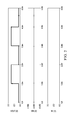
- FIG. 2 is an diagram depicting an example of the operation of the IC of FIG. 1 .
- the IC 100 includes an input pin VIN, an output pin VOUT, a ground pin GND, an enable pin VON, load switch Q 7 (which can, for example, be an NMOS transistor), a level shifter 102 , and a slew rate controller 104 .
- the level shifter 102 generally comprises a current control circuit (i.e., resistor R 1 ), a current mirror (i.e., NMOS transistors Q 3 and Q 2 ), transistor Q 1 (which can, for example, be a PMOS transistor), and a voltage divider or impedance network (i.e., resistors R 2 and R 3 ).
- the slew rate controller 104 generally comprises inverter 106 , transistors Q 5 and Q 6 (which can, for example, be a PMOS transistor and an NMOS transistor, respectively), and an impedance network (i.e., resistor R 4 ).
- the control circuit (which is generally formed by level shifter 104 and slew control circuit 104 ) uses the ground pin GND as a positive supply rail and the input pin VIN as an internal ground to generate a negative output voltage at output pin VOUT.
- a negative voltage is applied to the input pin VIN (i.e., ⁇ 5V), which means the ground pin GND, which is coupled to that ground (i.e., 0V), has a higher voltage than the input pin VIN.
- transistor Q 1 When the enable signal or voltage (applied to the enable pin VON) is less than the threshold voltage of the transistor Q 1 , transistor Q 1 is “off,” which pulls the input terminal of inverter 106 to the negative voltage (supplied through the input pin VIN) and which maintains the transistor Q 7 (i.e., the load switch) in an “off” state.
- transistor Q 1 turns “on.” With transistor Q 1 in an “on” state, a steering current is generated through resistor R 1 and transistor Q 3 (which is diode-connected). This steering current is mirrored through resistors R 2 and R 3 and transistor Q 1 .
- the intermediate signal or voltage (at the node between resistors R 2 and R 3 ) becomes a fraction of the “on” voltage of transistor Q 1 , which enables inverter 106 .
- the output of inverter 106 is applied to the gates of transistors Q 5 and Q 6 , and (collectively with resistor R 4 ) transistors Q 5 and Q 6 generate a slew-controlled intermediate signal or voltage at node N 1 , which (when the inverter 106 is enabled) is at ground.
- the output signal (at output pin VOUT) can be ground (applied to the ground pin GND) when transistor Q 1 is “off” and can be the negative voltage (applied to the input pin VIN) when transistor Q 1 is “on.”
- FIG. 2 an example of the operation of IC 100 can be seen.
- the input voltage applied to input pin VIN is ⁇ 5V.
- the enable signal which is applied to the enable pin VON
- the output signal from output pin VOUT toggles.
- the slew-controlled intermediate signal (at node N 1 ) toggles inversely with the output signal (at the output pint VOUT).
Landscapes
- Engineering & Computer Science (AREA)
- Computer Hardware Design (AREA)
- Physics & Mathematics (AREA)
- Computing Systems (AREA)
- General Engineering & Computer Science (AREA)
- Mathematical Physics (AREA)
- Logic Circuits (AREA)
Priority Applications (4)
| Application Number | Priority Date | Filing Date | Title |
|---|---|---|---|
| US13/786,151 US8854097B2 (en) | 2013-03-05 | 2013-03-05 | Load switch |
| EP14760468.0A EP2992607B1 (de) | 2013-03-05 | 2014-03-05 | Lastumschalter |
| PCT/US2014/020765 WO2014138243A1 (en) | 2013-03-05 | 2014-03-05 | Load switch |
| CN201480011810.5A CN105009453B (zh) | 2013-03-05 | 2014-03-05 | 负载开关 |
Applications Claiming Priority (1)
| Application Number | Priority Date | Filing Date | Title |
|---|---|---|---|
| US13/786,151 US8854097B2 (en) | 2013-03-05 | 2013-03-05 | Load switch |
Publications (2)
| Publication Number | Publication Date |
|---|---|
| US20140253194A1 US20140253194A1 (en) | 2014-09-11 |
| US8854097B2 true US8854097B2 (en) | 2014-10-07 |
Family
ID=51487106
Family Applications (1)
| Application Number | Title | Priority Date | Filing Date |
|---|---|---|---|
| US13/786,151 Active US8854097B2 (en) | 2013-03-05 | 2013-03-05 | Load switch |
Country Status (4)
| Country | Link |
|---|---|
| US (1) | US8854097B2 (de) |
| EP (1) | EP2992607B1 (de) |
| CN (1) | CN105009453B (de) |
| WO (1) | WO2014138243A1 (de) |
Families Citing this family (4)
| Publication number | Priority date | Publication date | Assignee | Title |
|---|---|---|---|---|
| TWI575858B (zh) * | 2015-10-07 | 2017-03-21 | 晨星半導體股份有限公司 | 切換式電壓轉換器 |
| US10468983B2 (en) * | 2015-11-05 | 2019-11-05 | Silicon Laboratories Inc. | Slew-rate controlled supply voltage switching |
| US11239831B2 (en) * | 2020-06-24 | 2022-02-01 | Texas Instruments Incorporated | Level shifter |
| CN113556119B (zh) * | 2021-09-18 | 2021-12-07 | 成都万创科技股份有限公司 | 一种防误接可切换式隔离型数字输入电路 |
Citations (2)
| Publication number | Priority date | Publication date | Assignee | Title |
|---|---|---|---|---|
| US7061291B2 (en) * | 2003-09-08 | 2006-06-13 | Texas Instruments Incorporated | Linear voltage tracking amplifier for negative supply slew rate control |
| US20090289692A1 (en) | 2008-05-21 | 2009-11-26 | Ting Huei Chen | Nagative voltage switch |
Family Cites Families (3)
| Publication number | Priority date | Publication date | Assignee | Title |
|---|---|---|---|---|
| CN100541569C (zh) * | 2004-08-30 | 2009-09-16 | 松下电器产业株式会社 | 驱动电路 |
| US7705630B1 (en) * | 2009-05-20 | 2010-04-27 | Ememory Technology Inc. | Negative voltage level shifter having simplified structure |
| CN102904565B (zh) * | 2012-10-09 | 2014-05-28 | 长安大学 | 一种用于dc-dc驱动的超低静态电流的电平移位电路 |
-
2013
- 2013-03-05 US US13/786,151 patent/US8854097B2/en active Active
-
2014
- 2014-03-05 CN CN201480011810.5A patent/CN105009453B/zh active Active
- 2014-03-05 EP EP14760468.0A patent/EP2992607B1/de active Active
- 2014-03-05 WO PCT/US2014/020765 patent/WO2014138243A1/en not_active Ceased
Patent Citations (2)
| Publication number | Priority date | Publication date | Assignee | Title |
|---|---|---|---|---|
| US7061291B2 (en) * | 2003-09-08 | 2006-06-13 | Texas Instruments Incorporated | Linear voltage tracking amplifier for negative supply slew rate control |
| US20090289692A1 (en) | 2008-05-21 | 2009-11-26 | Ting Huei Chen | Nagative voltage switch |
Also Published As
| Publication number | Publication date |
|---|---|
| US20140253194A1 (en) | 2014-09-11 |
| EP2992607A4 (de) | 2017-03-22 |
| EP2992607B1 (de) | 2018-08-29 |
| WO2014138243A1 (en) | 2014-09-12 |
| CN105009453A (zh) | 2015-10-28 |
| CN105009453B (zh) | 2018-08-28 |
| EP2992607A1 (de) | 2016-03-09 |
Similar Documents
| Publication | Publication Date | Title |
|---|---|---|
| US8847659B1 (en) | Systems and method for level shifters | |
| CN107342685B (zh) | Dcdc转换器 | |
| JP6082356B2 (ja) | 半導体装置 | |
| US9459639B2 (en) | Power supply circuit with control unit | |
| CN105807834B (zh) | 具有软启动和电流限制电路的n沟道输入对电压调节器 | |
| KR20170131452A (ko) | 파워 fet들의 캐스코드 스택용 드라이브 | |
| US8854097B2 (en) | Load switch | |
| US20170117888A1 (en) | Voltage comparison circuit | |
| US20160187900A1 (en) | Voltage regulator circuit and method for limiting inrush current | |
| US20170019090A1 (en) | Level shift circuit | |
| JP2019007823A (ja) | 半導体集積装置及びそのゲートスクリーニング試験方法 | |
| JP5806972B2 (ja) | 出力ドライバ回路 | |
| JP2018513613A5 (de) | ||
| JP2017041968A (ja) | 電力供給装置及びその制御方法 | |
| US10033358B2 (en) | Buffer circuit and voltage generator using the same | |
| EP3308240B1 (de) | Anlaufschaltung | |
| US7902904B2 (en) | Bias circuit scheme for improved reliability in high voltage supply with low voltage device | |
| US9075424B2 (en) | Compensation scheme to improve the stability of the operational amplifiers | |
| US20160182040A1 (en) | Audio switch circuit with slow turn-on | |
| US20150137856A1 (en) | Input circuit with mirroring | |
| US8816723B1 (en) | Buffer circuit | |
| US10320351B1 (en) | Switch for controlling a gain of an amplifier and method thereof | |
| JP2014085745A (ja) | 基準電圧生成回路 | |
| US10691151B2 (en) | Devices and methods for dynamic overvoltage protection in regulators | |
| JP5689778B2 (ja) | 入力回路 |
Legal Events
| Date | Code | Title | Description |
|---|---|---|---|
| AS | Assignment |
Owner name: TEXAS INSTRUMENTS INCORPORATED, TEXAS Free format text: ASSIGNMENT OF ASSIGNORS INTEREST;ASSIGNORS:SADATE, ALINE C.;GROSE, WILLIAM E.;REEL/FRAME:029938/0491 Effective date: 20130305 |
|
| STCF | Information on status: patent grant |
Free format text: PATENTED CASE |
|
| MAFP | Maintenance fee payment |
Free format text: PAYMENT OF MAINTENANCE FEE, 4TH YEAR, LARGE ENTITY (ORIGINAL EVENT CODE: M1551) Year of fee payment: 4 |
|
| MAFP | Maintenance fee payment |
Free format text: PAYMENT OF MAINTENANCE FEE, 8TH YEAR, LARGE ENTITY (ORIGINAL EVENT CODE: M1552); ENTITY STATUS OF PATENT OWNER: LARGE ENTITY Year of fee payment: 8 |
|
| MAFP | Maintenance fee payment |
Free format text: PAYMENT OF MAINTENANCE FEE, 12TH YEAR, LARGE ENTITY (ORIGINAL EVENT CODE: M1553); ENTITY STATUS OF PATENT OWNER: LARGE ENTITY Year of fee payment: 12 |