US8880928B2 - Multirate transmission system and method for parallel input data - Google Patents
Multirate transmission system and method for parallel input data Download PDFInfo
- Publication number
- US8880928B2 US8880928B2 US12/082,685 US8268508A US8880928B2 US 8880928 B2 US8880928 B2 US 8880928B2 US 8268508 A US8268508 A US 8268508A US 8880928 B2 US8880928 B2 US 8880928B2
- Authority
- US
- United States
- Prior art keywords
- data
- parallel
- clock
- parallel data
- information related
- Prior art date
- Legal status (The legal status is an assumption and is not a legal conclusion. Google has not performed a legal analysis and makes no representation as to the accuracy of the status listed.)
- Active, expires
Links
Images


Classifications
-
- G—PHYSICS
- G06—COMPUTING OR CALCULATING; COUNTING
- G06F—ELECTRIC DIGITAL DATA PROCESSING
- G06F13/00—Interconnection of, or transfer of information or other signals between, memories, input/output devices or central processing units
- G06F13/38—Information transfer, e.g. on bus
- G06F13/42—Bus transfer protocol, e.g. handshake; Synchronisation
- G06F13/4265—Bus transfer protocol, e.g. handshake; Synchronisation on a point to point bus
- G06F13/4278—Bus transfer protocol, e.g. handshake; Synchronisation on a point to point bus using an embedded synchronisation
-
- G—PHYSICS
- G06—COMPUTING OR CALCULATING; COUNTING
- G06F—ELECTRIC DIGITAL DATA PROCESSING
- G06F13/00—Interconnection of, or transfer of information or other signals between, memories, input/output devices or central processing units
- G06F13/38—Information transfer, e.g. on bus
- G06F13/40—Bus structure
- G06F13/4004—Coupling between buses
- G06F13/4027—Coupling between buses using bus bridges
- G06F13/4045—Coupling between buses using bus bridges where the bus bridge performs an extender function
Definitions
- the present invention relates to data transmission systems, in particular, transmission systems for transferring parallel data emanating from one location to a second, remote location, so as to replicate said parallel data at the remote location.
- Transmission systems for transferring parallel data from one location to a second, remote location have been used in what are sometimes called video extenders where the data emanating from a video output port on a computer or the like is transferred to a remote location for display on a remote monitor.
- video extenders where the data emanating from a video output port on a computer or the like is transferred to a remote location for display on a remote monitor.
- the present invention is directed to such an improved transmission system and is specifically directed to a multirate transmission system, wherein the parallel data clock rate is transferred on the same serial data stream as the serialized parallel data.
- a multirate transmission system sends data from a first location to a second location while being able to adjust to different parallel data clock rates of the incoming parallel data.
- the parallel data is received with an associated parallel data clock and is temporarily stored in a buffer.
- the data is written into the buffer at the rate of the parallel data clock.
- the data is read out of the buffer at an output rate so as to prevent the buffer from overflowing or underflowing.
- the read clock rate is greater than the write clock rate and thus during periods of time when data is not to be read, control characters are generated for such clock cycles.
- the overall parallel data and control characters are transferred to a serializer for generating a serial output data stream which can be transmitted to a remote location by various means, such as via an optical medium.
- the serialized data further contains information related to the parallel data clock rate.
- the serialized data is deserialized and converted back to parallel form and stored in a buffer.
- the data in the buffer is read out so as to prevent overflow and underflow.
- the parallel data is read out of the buffer at a parallel data clock rate based on the parallel data clock rate received in the serial data stream.
- the output of the buffer thereby corresponds to the parallel data received at the transmitter portion of the multirate transmission system.
- the multirate transmission system can further encode and decode the parallel data and control characters prior to sending the data on the serial data stream with decoding at the time of deserialization.
- An embodiment of the invention is specifically adapted for transmitting video according to the Digital Video Input (DVI) standard.
- DVI Digital Video Input
- a particular control character is generated by the transmitter portion to denote the boundaries of the parallel data to be serialized and this control character is used for retrieving the parallel data at the receiver portion of the transmission system.
- An embodiment of the multirate transmission system is able to transmit and receive DVI parallel data ranging from 25 MHz to 165 MHz.
- An embodiment of the transmission system determines the number of parallel data words (i.e., parallel data clock cycles) received by the transmitter over a predetermined period of time, where the information concerning this count is included in the serialized data sent to the receiver portion of the multirate transmission system so as to determine the parallel data clock rate at the receiver portion.
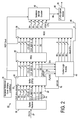
- FIG. 1 is an overall simplified block diagram of a multirate transmission system according to the present invention.
- FIG. 2 is a block diagram of the transmission of the transmitter portion of the multirate transmission system.
- FIG. 3 is a block diagram of the receiver portion of the multirate transmission system.
- a multirate transmission system 20 comprises a transmitter portion 22 and a receiver portion 24 linked together by a serial data link 26 , such as an optical fiber, coaxial cable, radio link, etc.
- the transmitter portion 22 receives incoming parallel input data 28 which is temporarily stored in a buffer 30 , such as a first in/first out (FIFO) buffer.
- the buffer can be implemented in various ways, including use of random access memory, registers and the like.
- the incoming parallel data is clocked into buffer (FIFO) 30 by means of a parallel data clock 32 .
- Data in the FIFO is read out of the FIFO on bus 31 by means of a serializer reference clock 34 having a frequency greater than the parallel data clock 32 .
- Multiplexer 36 receives synchronization and control data on bus 38 generated by a control module 40 along with parallel data on bus 31 read out of buffer 30 .
- the control module also interfaces with FIFO 30 and serializer 42 .
- the synchronization and control data are received during periods of time when parallel data is not being read from FIFO 30 . Therefore, the overall input data to the multiplexer is being clocked into the multiplexer at the serializer reference clock rate with data being either the parallel data from FIFO 30 or the synchronization and control data from control module 40 .
- Multiplexer 36 determines whether data from bus 31 or 38 is transferred to serializer 42 .
- the output from the multiplexer is provided to the serializer 42 under the control of the control module 40 in conjunction with the serializer reference clock 34 so as to generate a serial data stream for presentation on the serial link 26 .
- the serial link can be whatever length is necessary for communicating at a remote end at which the receiver portion 24 of the multirate transmission system 20 is located.
- the serializer clock rate is selected so as to be able to transmit the serial output data received from the multiplexer 36 .
- the receiver portion 24 of the multirate transmission system 20 effectively performs the reverse operation of the transmitter portion.
- a deserializer 44 under control of a deserializer reference clock 46 receives the incoming serial data stream and converts it into parallel data on output 48 under control of control module 50 .
- the parallel data is received by a demultiplexer 52 which under control of control module 50 generates a first parallel output 54 corresponding to the parallel data 28 received from the transmitter portion 22 and synchronization and control data 56 corresponding to the synchronization and control data 38 generated by the transmitter portion 22 .
- the parallel data 54 is written into a receive buffer 58 via recovered serial reference clock 64 .
- the output from buffer 58 is therefore a parallel output data stream 62 which corresponds to the parallel input data 28 received by the transmitter portion 22 .
- Data is clocked into buffer 58 from demultiplexer 52 based upon a recovered serializer reference clock 64 corresponding to the serializer reference clock 34 .
- the parallel data is read out of buffer 58 based on parallel data clock output 61 of parallel data output clock 60 .
- This parallel data output clock rate in one embodiment is derived from the ratio of the synchronization and control data 38 to the parallel data 31 from buffer 30 . It thereby insures that the parallel data read into buffer 58 from demultiplexer 52 is read from the buffer at a rate essentially corresponding to the parallel data clock rate 32 associated with the parallel data 28 received by transmitter portion 22 . Minor adjustments to the rate of the parallel data output clock 60 is made by means of control module 50 in association with flags 66 from buffer 58 . It can also be determined by counting the number of parallel data clock cycles within a predetermined length of time, such as 1 millisecond.
- the parallel output data 62 and parallel data output clock correspond essentially to the parallel input data 28 and parallel data input clock 32 with minimal jitter. Furthermore, a separate reference for purposes of establishing the rate of the parallel data output clock is eliminated since the rate of this clock is determined by the incoming serial data to the deserializer 44 as will be explained more fully below.
- FIG. 2 is a detailed block diagram of the transmitter portion 22 of the multirate transmission system 20 . It is specifically shown for an embodiment of the present invention for receipt of video data 27 corresponding to the Digital Video Input (DVI) standard.
- This data uses Transition Minimized Differential Signaling (TDMS) and is actually a type of high speed serial data.
- This data is converted into parallel data 28 and clock 32 by a digital receiver 29 .
- the parallel data can comprise a plurality if eight bit bytes 68 , 70 , and 72 and associated control information designated generally as 74 , including, for example, horizontal synchronization information, vertical synchronization information, and data enable (DE) information, as well as control information associated with the parallel data.
- DVI Digital Video Input
- TDMS Transition Minimized Differential Signaling
- the parallel input data clock 32 can, for the DVI standard, range from 25 MHz to 165 MHz. This information is clocked into buffer 30 via clock 32 . It is read out of buffer 30 via serializer reference clock 34 . Of course, any other type of data can be received at its own data clock rate. It should be noted that types of data received by the multirate transmission system 20 can therefore be anything as long as the data can be converted into parallel data 28 with associated clock data 32 . Thus, the digital receiver 29 and digital transmitter 102 shown respectively in FIGS. 2 and 3 associated with the embodiment for transmitting and receiving data according to the DVI standard, need not form part of the multirate transmission system.
- the serializer reference clock has a data rate of 180 MHz (that is, greater than the maximum data rate of the incoming DVI data).
- the parallel data 28 is clocked into buffer 30 based upon the parallel data clock signal 32 in conjunction with the write enable signal 76 from control logic module 40 .
- Buffer 30 has independent read clock capability; that is, the read clock can be different from the write clock and thus data stored in buffer 30 can be read from it by means of the serializer reference clock 34 which operates at a higher clock rate than the clock associated with the incoming parallel data.
- the buffer 30 is only read when enabled to do so by the read enable signal 78 from control logic module 40 , in an arrangement that insures that there is neither underflow or overflow of the data within buffer 30 .
- the serializer reference clock 34 in conjunction with control module 40 generates control characters on data busses 80 so that these control characters are received by multiplexer 36 .
- Control module 40 can generate information related to parallel data clock 32 for transmission by counting the number of parallel data clock cycles for a predetermined length of time, such as 1 millisecond.
- Serializer 42 is connected to output busses 84 from multiplexer 36 under the control of K/data control bus 86 from control logic module 40 .
- K/data control bus 86 informs serializer 42 whether the data from multiplexer 36 corresponds to the parallel data 28 or to the control characters generated by control logic module 40 as received by multiplexer 36 via data busses 80 .
- serializer 42 also encodes the received parallel data, including the control characters via an encoding scheme, such as the 8B/10B encoding scheme well-known in the art. Other encoding/decoding schemes can, of course, be used.
- the resulting encoded serialized output is presented on output line 88 for presentation to optical module 90 for generating a serialized output on serial data medium 26 .
- the optical module has a 7.2 GHz data rate so as to correspond to the maximum parallel data rate of the serializer reference clock 34 times the number of parallel data bits received by serializer 42 which, in this particular embodiment, is 40 bits.
- other means for transmitting a serial output data stream are possible, including the use of coaxial cable or a radio frequency output module instead of the optical module 30 . Such alternative means for generating an outgoing serial data stream for long distance transmission are well-known in the art.
- FIG. 3 is a detailed block diagram of the receiver portion 24 of the multirate transmission system and therefore includes a corresponding optical module 92 for receipt of the serial data stream via serial media 26 .
- the deserializer reference clock 46 has a nominal frequency corresponding to the serializer reference clock 34 which, in this particular embodiment, is 180 MHz.
- Deserializer 44 in this particular embodiment therefore not only deserializes the incoming data from the optical module 32 , but also decodes the data, which in this particular embodiment is via the 8B/10B decoding scheme.
- the data deserialized by deserializer 44 is output on parallel output data busses 48 correspond to the incoming DVI data and control information, while the control characters received for those periods of time when the DVI data is not present are transferred to control module 50 via bus 56 under control of the K/data bus 94 .
- Control module 50 via the multiplexer (MUX) control line 96 and the recovered serializer clock 64 , control multiplexer 52 with respect to writing of the parallel DVI data into the demultiplexer.
- the output of the demultiplexer with respect to the parallel data (DVI data 28 ) is transferred to the buffer 58 , such as a FIFO type buffer, which is also under the control of the control logic module 50 via the write enable (WE) signal 98 .
- the buffer 58 such as a FIFO type buffer
- the FIFO output flags 66 are transferred to the control logic module 50 to enable the timing of the read enable (RE) signal 100 which, in conjunction with the parallel data output clock signal 61 of the parallel data output clock 60 , insures that the data read from the FIFO buffer 58 is at a data rate corresponding to the incoming data rate of the parallel data 28 , and further to insure that the buffer does not underflow or overflow.
- the rate of the parallel data output clock signal 61 is adjusted by comparison of this clock rate to the information related to the parallel data clock rate as transmitted in the serial data stream.
- the output 62 of the FIFO buffer 58 and the parallel data clock output signal 61 are transferred to a DVI digital transmitter 102 for generating a DVI TMDS data output 104 which corresponds to the DVI input data 27 received by digital receiver 29 at the front end of transmitter portion 22 of multirate transmission system 20 .
- the overall result of the multirate transmission system is therefore to generate a parallel data output at the receiver portion which corresponds to the parallel data input received by the transmitter portion.
- the present invention achieves this objective with recapturing of the data rate of the parallel input data without the need for any separate transmission of clocking information aside from the information transmitted in the serial data stream between the transmitter portion and the receiver portion.
- the control logic module 50 in association with the parallel data output clock 60 , minor adjustments in the read rate of the parallel data from buffer 58 are made so as to minimize the jitter associated with the parallel data output clock rate 61 corresponding to the input rate of the parallel data arriving at the transmitter portion of the multirate transmission system. This minimizing of jitter is essential for some applications, including DVI applications.
- the parallel input data clock rate is derivable from the received data stream to the deserializer 44 by the control module comparing the percentage of parallel data to the percentage of control characters received via the deserializer.
- the parallel data clock rate has a frequency of 0.5 ⁇ 180 MHz or 90 MHz.
- the overall result is a multirate transmission system which can be used with incoming parallel input data that can range over a wide frequency range for any particular application. If the input frequency of the parallel input data varies, resynchronization of the multirate transmission system is easily obtainable since the information necessary for recovering the input parallel data is contained within the serial data stream received by the deserializer at the receiver portion.
- one method of measuring the parallel data clock is by counting the number of parallel data clock cycles during a one millisecond time period. This function is performed by controller 40 .
- a 24 bit value is read by a local central processing unit (CPU) of the control module and transmitted by the serializer and the optical link 26 during a control phase of the transmission.
- CPU central processing unit
- the value from the transmitter portion is read and stored in memory of control module 50 for comparison to the rate of the parallel data output clock 60 .
- this value can be determined by counting the number of parallel data words in a one millisecond period.
- the two values for the receiver and transmitter are compared and the parallel data output clock is adjusted using a procedure as set forth in Table 1 below.
- the adjustments can be made during every vertical synchronization period of video data, which is usually at a frequency of 60 Hz.
- the underlying concept of this methodology is that if the receiver clock is faster than the transmitter clock, then the CPU at the receiver portion slows down the clock generator, (parallel data output clock), and conversely, if the receiver clock is too slow, the control module speeds up the clock generator.
- Enhancements can be made to check if the values are in range, as well as a procedure to adjust the clock generator in non-linear steps to achieve faster matching than otherwise possible. This is done by use of a COURSE and MEDIUM adjustment phases (see Table 1).
- a FINE phase uses the FIFO data count from buffer 58 as an indication of how fast or slow the data is being read out.
- the FIFO data word should be approximately one half of the FIFO size in order to allow for “rubberbanding” of the output data.
- the FIFO data word is continually monitored and the clock is continually adjusted to compensate for data bursting and source clock dithering. When two clock counts cannot be adjusted within a normal range, the procedure reverts back to either COURSE or MEDIUM mode in order to readjust the regenerated clock signal. This procedure can be used to detect when a screen resolution has changed in the incoming DVI video data.
- Another embodiment of the present invention can receive data corresponding to the Universal Serial Bus standard, including the USB 2.0 standard, for purposes of transmitting keyboard, mouse and audio information or any other information that supports the USB standard.
- serial link and associated optical transmitter and receiver can be implemented according to the XAUI standard for connecting 10 Gigabit Ethernet (10 GbE) ports to each other. It can also be used for 10 G XFP (small form factor pluggable) hot-swappable protocol-independent optical transceiver applications, including those for DVI dual link applications.
- XAUI XAUI standard for connecting 10 Gigabit Ethernet (10 GbE) ports to each other. It can also be used for 10 G XFP (small form factor pluggable) hot-swappable protocol-independent optical transceiver applications, including those for DVI dual link applications.
- the buffer, register, multiplexer, serializer and control logic module of transmitter portion 22 can be fabricated from a field programmable gate array.
- Optical modules 90 and 92 can be a small form factor pluggable (SFP) optical transceiver.
- the deserializer, multiplexer, buffer, and control logic module can also be fabricated from field programmable gate arrays.
- Parallel data output clock 60 can be fabricated from Analog Device part no. AD9910, having a clock range of from 0 to 400 MHz in 0.25 Hz increments.
- the control modules can also be fabricated from control processing units with associated memory for program control (including implementation of the parallel data clock control information).
- Digital receiver 29 can be fabricated from a receiver manufactured by Silicon Image, part number 7171 and digital transmitter 102 can be fabricated from a transmitter manufactured by Silicon Image, part number 7170.
Landscapes
- Engineering & Computer Science (AREA)
- Theoretical Computer Science (AREA)
- General Engineering & Computer Science (AREA)
- Physics & Mathematics (AREA)
- General Physics & Mathematics (AREA)
- Computer Hardware Design (AREA)
- Information Transfer Systems (AREA)
- Synchronisation In Digital Transmission Systems (AREA)
Priority Applications (7)
| Application Number | Priority Date | Filing Date | Title |
|---|---|---|---|
| US12/082,685 US8880928B2 (en) | 2008-04-11 | 2008-04-11 | Multirate transmission system and method for parallel input data |
| PL09730817T PL2274679T3 (pl) | 2008-04-11 | 2009-03-02 | System transmisji o wielu szybkościach dla wejściowych danych równoległych |
| EP09730817.5A EP2274679B1 (en) | 2008-04-11 | 2009-03-02 | Multirate transmission system for parallel input data |
| ES09730817T ES2430387T3 (es) | 2008-04-11 | 2009-03-02 | Sistema de transmisión de múltiples frecuencias para datos de entrada paralelos |
| DK09730817.5T DK2274679T3 (da) | 2008-04-11 | 2009-03-02 | Flerhastighedstransmissionssystem til parallelle indgangsdata |
| PCT/IB2009/000393 WO2009125260A1 (en) | 2008-04-11 | 2009-03-02 | Multirate transmission system for parallel input data |
| PT97308175T PT2274679E (pt) | 2008-04-11 | 2009-03-02 | Sistema de transmissão multifrequência para dados paralelos de entrada |
Applications Claiming Priority (1)
| Application Number | Priority Date | Filing Date | Title |
|---|---|---|---|
| US12/082,685 US8880928B2 (en) | 2008-04-11 | 2008-04-11 | Multirate transmission system and method for parallel input data |
Publications (2)
| Publication Number | Publication Date |
|---|---|
| US20090259878A1 US20090259878A1 (en) | 2009-10-15 |
| US8880928B2 true US8880928B2 (en) | 2014-11-04 |
Family
ID=40668399
Family Applications (1)
| Application Number | Title | Priority Date | Filing Date |
|---|---|---|---|
| US12/082,685 Active 2033-01-26 US8880928B2 (en) | 2008-04-11 | 2008-04-11 | Multirate transmission system and method for parallel input data |
Country Status (7)
| Country | Link |
|---|---|
| US (1) | US8880928B2 (pl) |
| EP (1) | EP2274679B1 (pl) |
| DK (1) | DK2274679T3 (pl) |
| ES (1) | ES2430387T3 (pl) |
| PL (1) | PL2274679T3 (pl) |
| PT (1) | PT2274679E (pl) |
| WO (1) | WO2009125260A1 (pl) |
Cited By (2)
| Publication number | Priority date | Publication date | Assignee | Title |
|---|---|---|---|---|
| US10366663B2 (en) | 2016-02-18 | 2019-07-30 | Synaptics Incorporated | Dithering a clock used to update a display to mitigate display artifacts |
| WO2020014557A1 (en) | 2018-07-12 | 2020-01-16 | Thinklogical Llc | Computing and communication module with vdi client and kvm extender |
Families Citing this family (11)
| Publication number | Priority date | Publication date | Assignee | Title |
|---|---|---|---|---|
| US8510487B2 (en) * | 2010-02-11 | 2013-08-13 | Silicon Image, Inc. | Hybrid interface for serial and parallel communication |
| US8577666B2 (en) * | 2010-04-21 | 2013-11-05 | Vixs Systems, Inc. | Clock synchronization in a modular circuit emulation system |
| US20120331194A1 (en) * | 2011-06-23 | 2012-12-27 | Apple Inc. | Interface extender for portable electronic devices |
| US8760188B2 (en) | 2011-06-30 | 2014-06-24 | Silicon Image, Inc. | Configurable multi-dimensional driver and receiver |
| US9071243B2 (en) | 2011-06-30 | 2015-06-30 | Silicon Image, Inc. | Single ended configurable multi-mode driver |
| KR102025338B1 (ko) * | 2011-12-28 | 2019-09-26 | 삼성전자 주식회사 | 신호 처리 장치, 이를 구비한 디스플레이 장치 및 신호 처리 방법 |
| US8891405B2 (en) | 2012-07-18 | 2014-11-18 | International Business Machines Corporation | Integrated device management over Ethernet network |
| US10108577B2 (en) * | 2015-01-06 | 2018-10-23 | Intel Corporation | Digital interconnects with protocol-agnostic repeaters |
| US10090993B2 (en) * | 2016-08-19 | 2018-10-02 | Ali Corporation | Packaged circuit |
| CN109977059B (zh) * | 2019-03-28 | 2020-10-27 | 清华大学 | 一种用于串行接口的并行数据位宽变换电路 |
| CN116545582B (zh) * | 2023-04-27 | 2026-03-27 | 山东云海国创云计算装备产业创新中心有限公司 | 基于串行收发器的数据传输方法、收发器、介质及设备 |
Citations (10)
| Publication number | Priority date | Publication date | Assignee | Title |
|---|---|---|---|---|
| US4558445A (en) | 1984-04-18 | 1985-12-10 | The United States Of America As Represented By The Secretary Of The Air Force | Applique rate converter |
| US4885746A (en) * | 1983-10-19 | 1989-12-05 | Fujitsu Limited | Frequency converter |
| US6094432A (en) * | 1996-11-04 | 2000-07-25 | Lg Information & Communications, Ltd. | Apparatus for and method of segmenting and reassembling constant bit rate traffic in asynchronous transfer mode network |
| US20030091039A1 (en) | 2001-11-15 | 2003-05-15 | International Business Machines Corporation | Modification of bus protocol packet for serial data synchronization |
| US6574731B1 (en) | 1999-03-05 | 2003-06-03 | Hewlett-Packard Company | Transmitting data words |
| US20030214977A1 (en) | 2002-02-28 | 2003-11-20 | Jerchen Kuo | Clock distribution in a communications network |
| US7356756B1 (en) * | 2004-08-20 | 2008-04-08 | Altera Corporation | Serial communications data path with optional features |
| US7539209B2 (en) * | 2003-03-05 | 2009-05-26 | Ciena Corporation | Method and device for preserving pacing information across a transport medium |
| US7684437B2 (en) * | 2005-03-23 | 2010-03-23 | Analog Devices, Inc. | System and method providing fixed rate transmission for digital visual interface and high-definition multimedia interface applications |
| US7830924B2 (en) * | 2006-12-13 | 2010-11-09 | Hitachi Communication Technologies, Ltd. | Stuffing and destuffing operations when mapping low-order client signals into high-order transmission frames |
-
2008
- 2008-04-11 US US12/082,685 patent/US8880928B2/en active Active
-
2009
- 2009-03-02 EP EP09730817.5A patent/EP2274679B1/en active Active
- 2009-03-02 ES ES09730817T patent/ES2430387T3/es active Active
- 2009-03-02 WO PCT/IB2009/000393 patent/WO2009125260A1/en not_active Ceased
- 2009-03-02 DK DK09730817.5T patent/DK2274679T3/da active
- 2009-03-02 PL PL09730817T patent/PL2274679T3/pl unknown
- 2009-03-02 PT PT97308175T patent/PT2274679E/pt unknown
Patent Citations (10)
| Publication number | Priority date | Publication date | Assignee | Title |
|---|---|---|---|---|
| US4885746A (en) * | 1983-10-19 | 1989-12-05 | Fujitsu Limited | Frequency converter |
| US4558445A (en) | 1984-04-18 | 1985-12-10 | The United States Of America As Represented By The Secretary Of The Air Force | Applique rate converter |
| US6094432A (en) * | 1996-11-04 | 2000-07-25 | Lg Information & Communications, Ltd. | Apparatus for and method of segmenting and reassembling constant bit rate traffic in asynchronous transfer mode network |
| US6574731B1 (en) | 1999-03-05 | 2003-06-03 | Hewlett-Packard Company | Transmitting data words |
| US20030091039A1 (en) | 2001-11-15 | 2003-05-15 | International Business Machines Corporation | Modification of bus protocol packet for serial data synchronization |
| US20030214977A1 (en) | 2002-02-28 | 2003-11-20 | Jerchen Kuo | Clock distribution in a communications network |
| US7539209B2 (en) * | 2003-03-05 | 2009-05-26 | Ciena Corporation | Method and device for preserving pacing information across a transport medium |
| US7356756B1 (en) * | 2004-08-20 | 2008-04-08 | Altera Corporation | Serial communications data path with optional features |
| US7684437B2 (en) * | 2005-03-23 | 2010-03-23 | Analog Devices, Inc. | System and method providing fixed rate transmission for digital visual interface and high-definition multimedia interface applications |
| US7830924B2 (en) * | 2006-12-13 | 2010-11-09 | Hitachi Communication Technologies, Ltd. | Stuffing and destuffing operations when mapping low-order client signals into high-order transmission frames |
Cited By (2)
| Publication number | Priority date | Publication date | Assignee | Title |
|---|---|---|---|---|
| US10366663B2 (en) | 2016-02-18 | 2019-07-30 | Synaptics Incorporated | Dithering a clock used to update a display to mitigate display artifacts |
| WO2020014557A1 (en) | 2018-07-12 | 2020-01-16 | Thinklogical Llc | Computing and communication module with vdi client and kvm extender |
Also Published As
| Publication number | Publication date |
|---|---|
| WO2009125260A1 (en) | 2009-10-15 |
| EP2274679B1 (en) | 2013-08-21 |
| ES2430387T3 (es) | 2013-11-20 |
| US20090259878A1 (en) | 2009-10-15 |
| PL2274679T3 (pl) | 2014-01-31 |
| DK2274679T3 (da) | 2013-11-25 |
| EP2274679A1 (en) | 2011-01-19 |
| PT2274679E (pt) | 2013-11-19 |
Similar Documents
| Publication | Publication Date | Title |
|---|---|---|
| US8880928B2 (en) | Multirate transmission system and method for parallel input data | |
| KR101514413B1 (ko) | 정보 스큐 및 리던던트 콘트롤 정보에 의한 데이터 송신 장치 및 방법 | |
| US9485514B2 (en) | System and method for compressing video and reformatting the compressed video to simulate uncompressed video with a lower bandwidth | |
| US6693895B1 (en) | Multiple synchronous data stream format for an optical data link | |
| US6954491B1 (en) | Methods and systems for sending side-channel data during data inactive period | |
| US7600061B2 (en) | Data transfer control device and electronic instrument | |
| CN1658596B (zh) | Fifo模块以及具有fifo模块的延迟均衡电路和速率匹配电路 | |
| US11546241B2 (en) | Technologies for timestamping with error correction | |
| US20110064413A1 (en) | Method and Apparatus for Optical Wireless Communication | |
| US20060143335A1 (en) | System for transmission of synchronous video with compression through channels with varying transmission delay | |
| US9686536B2 (en) | Method and apparatus for aggregation and streaming of monitoring data | |
| US10680963B2 (en) | Circuit and method for credit-based flow control | |
| US7792152B1 (en) | Scheme for transmitting video and audio data of variable formats over a serial link of a fixed data rate | |
| US10404627B2 (en) | Multi-function, multi-protocol FIFO for high-speed communication | |
| JP4781688B2 (ja) | 映像信号伝送方法及び映像信号伝送装置 | |
| CN117640871B (zh) | 一种SDI接口至eDP接口的数据转换装置及方法 | |
| CN116095257B (zh) | 一种多路hdmi视频切换显示系统 | |
| KR20220144643A (ko) | 정렬 마커 기능을 포함하는 탄성 버퍼를 이용한 데이터 전송 방법 및 장치 | |
| GB2339654A (en) | Optical data link system |
Legal Events
| Date | Code | Title | Description |
|---|---|---|---|
| AS | Assignment |
Owner name: LOGICAL SOLUTIONS INC., THE, CONNECTICUT Free format text: ASSIGNMENT OF ASSIGNORS INTEREST;ASSIGNORS:REMLIN, MARK;ENGLER, MICHAEL;REEL/FRAME:020964/0521 Effective date: 20080505 |
|
| AS | Assignment |
Owner name: THINKLOGICAL INC., CONNECTICUT Free format text: ASSIGNMENT OF ASSIGNORS INTEREST;ASSIGNOR:LOGICAL SOLUTIONS INC., THE;REEL/FRAME:022590/0584 Effective date: 20090203 |
|
| AS | Assignment |
Owner name: THINKLOGICAL, LLC,CONNECTICUT Free format text: ASSIGNMENT OF ASSIGNORS INTEREST;ASSIGNOR:XTL COMPANY (F/K/A THINKLOGICAL, INC.);REEL/FRAME:024065/0554 Effective date: 20100309 Owner name: THINKLOGICAL, LLC, CONNECTICUT Free format text: ASSIGNMENT OF ASSIGNORS INTEREST;ASSIGNOR:XTL COMPANY (F/K/A THINKLOGICAL, INC.);REEL/FRAME:024065/0554 Effective date: 20100309 |
|
| STCF | Information on status: patent grant |
Free format text: PATENTED CASE |
|
| AS | Assignment |
Owner name: JPMORGAN CHASE BANK, N.A., AS ADMINISTRATIVE AGENT Free format text: SECURITY INTEREST;ASSIGNOR:THINKLOGICAL, LLC;REEL/FRAME:043731/0574 Effective date: 20170928 |
|
| MAFP | Maintenance fee payment |
Free format text: PAYMENT OF MAINTENANCE FEE, 4TH YR, SMALL ENTITY (ORIGINAL EVENT CODE: M2551) Year of fee payment: 4 |
|
| FEPP | Fee payment procedure |
Free format text: ENTITY STATUS SET TO UNDISCOUNTED (ORIGINAL EVENT CODE: BIG.) |
|
| MAFP | Maintenance fee payment |
Free format text: PAYMENT OF MAINTENANCE FEE, 8TH YEAR, LARGE ENTITY (ORIGINAL EVENT CODE: M1552); ENTITY STATUS OF PATENT OWNER: LARGE ENTITY Year of fee payment: 8 |