US8890134B2 - Organic photoelectric material and organic photoelectric device and image sensor - Google Patents
Organic photoelectric material and organic photoelectric device and image sensor Download PDFInfo
- Publication number
- US8890134B2 US8890134B2 US13/930,445 US201313930445A US8890134B2 US 8890134 B2 US8890134 B2 US 8890134B2 US 201313930445 A US201313930445 A US 201313930445A US 8890134 B2 US8890134 B2 US 8890134B2
- Authority
- US
- United States
- Prior art keywords
- organic photoelectric
- photoelectric device
- layer
- electrode
- photoelectric material
- Prior art date
- Legal status (The legal status is an assumption and is not a legal conclusion. Google has not performed a legal analysis and makes no representation as to the accuracy of the status listed.)
- Active
Links
- 0 [C-]#[N+]C(=C*C=C(C#N)C#N)[N+]#[C-] Chemical compound [C-]#[N+]C(=C*C=C(C#N)C#N)[N+]#[C-] 0.000 description 4
- JPUQRVJYPJHVBF-BOFXDRFVSA-N C1=CC2=C(S1)C1=C(S2)C2=C(C=CS2)S1.C1=CC2=C(S1)C1=C(S2)C2=C(S1)C1=C(C=CS1)S2.C1=CC2=C(S1)C1=C(S2)C2=C(S1)C1=C(S2)C2=C(C=CS2)S1.C1=CC2=C(S1)C1=C(S2)C2=C(S1)C1=C(S2)C2=C(S1)C1=C(C=CS1)S2.C1=CC2=C(S1)C1=CC3=C(C=C1C2)C1=C(C=C2C(=C1)CC1=C2SC=C1)C3.C1=CC2=C(S1)C1=CC3=C(C=C1C2)C1=C(C=CS1)C3.CC.CC=C(C#N)C#N.CC=C(C#N)C#N.CC=C(C#N)C#N.CC=C(C#N)C#N.CC=C(C#N)C#N.CC=C(C#N)C#N.[C-]#[N+]/C(C#N)=C/C.[C-]#[N+]C(=CC)[N+]#[C-].[C-]#[N+]C(=CC)[N+]#[C-].[C-]#[N+]C(=CC)[N+]#[C-].[C-]#[N+]C(=CC)[N+]#[C-].[C-]#[N+]C(=CC)[N+]#[C-] Chemical compound C1=CC2=C(S1)C1=C(S2)C2=C(C=CS2)S1.C1=CC2=C(S1)C1=C(S2)C2=C(S1)C1=C(C=CS1)S2.C1=CC2=C(S1)C1=C(S2)C2=C(S1)C1=C(S2)C2=C(C=CS2)S1.C1=CC2=C(S1)C1=C(S2)C2=C(S1)C1=C(S2)C2=C(S1)C1=C(C=CS1)S2.C1=CC2=C(S1)C1=CC3=C(C=C1C2)C1=C(C=C2C(=C1)CC1=C2SC=C1)C3.C1=CC2=C(S1)C1=CC3=C(C=C1C2)C1=C(C=CS1)C3.CC.CC=C(C#N)C#N.CC=C(C#N)C#N.CC=C(C#N)C#N.CC=C(C#N)C#N.CC=C(C#N)C#N.CC=C(C#N)C#N.[C-]#[N+]/C(C#N)=C/C.[C-]#[N+]C(=CC)[N+]#[C-].[C-]#[N+]C(=CC)[N+]#[C-].[C-]#[N+]C(=CC)[N+]#[C-].[C-]#[N+]C(=CC)[N+]#[C-].[C-]#[N+]C(=CC)[N+]#[C-] JPUQRVJYPJHVBF-BOFXDRFVSA-N 0.000 description 3
- WMCUQMPVYSYHQQ-UHFFFAOYSA-N *.B.CCOC(=O)C1=C(C2=CC=CS2)C=C(CC)C(C2=CC=CS2)=C1.O=C=O.O=C=O.[H]C1=CC(C2=CC=CS2)=C(C(=O)O)C=C1C1=CC=CS1 Chemical compound *.B.CCOC(=O)C1=C(C2=CC=CS2)C=C(CC)C(C2=CC=CS2)=C1.O=C=O.O=C=O.[H]C1=CC(C2=CC=CS2)=C(C(=O)O)C=C1C1=CC=CS1 WMCUQMPVYSYHQQ-UHFFFAOYSA-N 0.000 description 1
- DHYOYENFLPEYFI-UHFFFAOYSA-N *.CCOC(=O)C1=C(C2=CC=CS2)C=C(CC)C(C2=CC=CS2)=C1.CCOC(=O)C1=CC(Br)=C(C(=O)OCC)C=C1Br.O=C=O.OB(O)C1=CC=CS1 Chemical compound *.CCOC(=O)C1=C(C2=CC=CS2)C=C(CC)C(C2=CC=CS2)=C1.CCOC(=O)C1=CC(Br)=C(C(=O)OCC)C=C1Br.O=C=O.OB(O)C1=CC=CS1 DHYOYENFLPEYFI-UHFFFAOYSA-N 0.000 description 1
- BGOPJMAGKVFNAZ-PSZXADNCSA-K B.C.Cl[Al](Cl)Cl.O=C1C2=CC3=C(C=C2C2=C1C=CS2)C(=O)C1=C3C=CS1.O=C=O.O=CClC1=CC(C2=CC=CS2)=C(C(=O)Cl)C=C1C1=CC=CS1.[2HH].[H]C1=CC(C2=CC=CS2)=C(C(=O)O)C=C1C1=CC=CS1 Chemical compound B.C.Cl[Al](Cl)Cl.O=C1C2=CC3=C(C=C2C2=C1C=CS2)C(=O)C1=C3C=CS1.O=C=O.O=CClC1=CC(C2=CC=CS2)=C(C(=O)Cl)C=C1C1=CC=CS1.[2HH].[H]C1=CC(C2=CC=CS2)=C(C(=O)O)C=C1C1=CC=CS1 BGOPJMAGKVFNAZ-PSZXADNCSA-K 0.000 description 1
- ASRHICFCKHXCHV-SGNQUONSSA-N C.C1=CC2=C(CC3=C2C=C2CC4=C(SC=C4)C2=C3)S1.O=C1C2=CC3=C(C=C2C2=C1C=CS2)C(=O)C1=C3C=CS1.[2HH] Chemical compound C.C1=CC2=C(CC3=C2C=C2CC4=C(SC=C4)C2=C3)S1.O=C1C2=CC3=C(C=C2C2=C1C=CS2)C(=O)C1=C3C=CS1.[2HH] ASRHICFCKHXCHV-SGNQUONSSA-N 0.000 description 1
- CYYFEXLDDAPXDN-UHFFFAOYSA-N C.CC1(C)C2=CC3=C(C=C2C2=C1C=C(C=O)S2)C(C)(C)C1=C3C=C(C=O)S1.CC1(C)C2=CC3=C(C=C2C2=C1C=CS2)C(C)(C)C1=C3C=CS1.F Chemical compound C.CC1(C)C2=CC3=C(C=C2C2=C1C=C(C=O)S2)C(C)(C)C1=C3C=C(C=O)S1.CC1(C)C2=CC3=C(C=C2C2=C1C=CS2)C(C)(C)C1=C3C=CS1.F CYYFEXLDDAPXDN-UHFFFAOYSA-N 0.000 description 1
- KHRWKIKHHBQWRE-AKCGCNCJSA-N C.CC1(C)C2=CC3=C(C=C2C2=C1C=C(C=O)S2)C(C)(C)C1=C3C=C(C=O)S1.[C-]#[N+]/C(C#N)=C\C1=CC2=C(S1)C1=C/C3=C(\C=C/1C2(C)C)C1=C(SC(/C=C(\C#N)[N+]#[C-])=C1)C3(C)C.[C-]#[N+]CC#N.[HH] Chemical compound C.CC1(C)C2=CC3=C(C=C2C2=C1C=C(C=O)S2)C(C)(C)C1=C3C=C(C=O)S1.[C-]#[N+]/C(C#N)=C\C1=CC2=C(S1)C1=C/C3=C(\C=C/1C2(C)C)C1=C(SC(/C=C(\C#N)[N+]#[C-])=C1)C3(C)C.[C-]#[N+]CC#N.[HH] KHRWKIKHHBQWRE-AKCGCNCJSA-N 0.000 description 1
- JXPQJNUGHRINGZ-BOFXDRFVSA-N C1=CC2=C(C1)C1=C(S2)C2=C(S1)C1=C(C=CS1)S2.C1=CC2=C(S1)C1=C(S2)C2=C(C=CS2)S1.C1=CC2=C(S1)C1=C(S2)C2=C(S1)C1=C(S2)C2=C(C=CS2)S1.C1=CC2=C(S1)C1=C(S2)C2=C(S1)C1=C(S2)C2=C(S1)C1=C(C=CS1)S2.C1=CC2=C(S1)C1=CC3=C(C=C1C2)C1=C(C=C2C(=C1)CC1=C2SC=C1)C3.C1=CC2=C(S1)C1=CC3=C(C=C1C2)C1=C(C=CS1)C3.CC.CC=C(C#N)C#N.CC=C(C#N)C#N.CC=C(C#N)C#N.CC=C(C#N)C#N.CC=C(C#N)C#N.CC=C(C#N)C#N.[C-]#[N+]/C(C#N)=C/C.[C-]#[N+]C(=CC)[N+]#[C-].[C-]#[N+]C(=CC)[N+]#[C-].[C-]#[N+]C(=CC)[N+]#[C-].[C-]#[N+]C(=CC)[N+]#[C-].[C-]#[N+]C(=CC)[N+]#[C-] Chemical compound C1=CC2=C(C1)C1=C(S2)C2=C(S1)C1=C(C=CS1)S2.C1=CC2=C(S1)C1=C(S2)C2=C(C=CS2)S1.C1=CC2=C(S1)C1=C(S2)C2=C(S1)C1=C(S2)C2=C(C=CS2)S1.C1=CC2=C(S1)C1=C(S2)C2=C(S1)C1=C(S2)C2=C(S1)C1=C(C=CS1)S2.C1=CC2=C(S1)C1=CC3=C(C=C1C2)C1=C(C=C2C(=C1)CC1=C2SC=C1)C3.C1=CC2=C(S1)C1=CC3=C(C=C1C2)C1=C(C=CS1)C3.CC.CC=C(C#N)C#N.CC=C(C#N)C#N.CC=C(C#N)C#N.CC=C(C#N)C#N.CC=C(C#N)C#N.CC=C(C#N)C#N.[C-]#[N+]/C(C#N)=C/C.[C-]#[N+]C(=CC)[N+]#[C-].[C-]#[N+]C(=CC)[N+]#[C-].[C-]#[N+]C(=CC)[N+]#[C-].[C-]#[N+]C(=CC)[N+]#[C-].[C-]#[N+]C(=CC)[N+]#[C-] JXPQJNUGHRINGZ-BOFXDRFVSA-N 0.000 description 1
- RRYOGZSDOBEVFI-UHFFFAOYSA-N C1=CC2=C(CC3=C2C=C2CC4=C(SC=C4)C2=C3)S1.C1CCOC1.CC1(C)C2=CC3=C(C=C2C2=C1C=CS2)C(C)(C)C1=C3C=CS1.F Chemical compound C1=CC2=C(CC3=C2C=C2CC4=C(SC=C4)C2=C3)S1.C1CCOC1.CC1(C)C2=CC3=C(C=C2C2=C1C=CS2)C(C)(C)C1=C3C=CS1.F RRYOGZSDOBEVFI-UHFFFAOYSA-N 0.000 description 1
- XMRBMQPURQKLRN-UHFFFAOYSA-N CC1(C)c(cc(c(c([n]2C)c3)cc(C4(C)C)c3-c3c4cc(C=C(C#N)C#N)[s]3)c2c2)c2-c2c1cc(C=C(C#N)C#N)[s]2 Chemical compound CC1(C)c(cc(c(c([n]2C)c3)cc(C4(C)C)c3-c3c4cc(C=C(C#N)C#N)[s]3)c2c2)c2-c2c1cc(C=C(C#N)C#N)[s]2 XMRBMQPURQKLRN-UHFFFAOYSA-N 0.000 description 1
- NZLBFYJQRRKIGQ-UFWORHAWSA-N [C-]#[N+]/C(C#N)=C/C1=C/C2=C(S1)/C1=C/C3=C(/C=C/1C2(C)C)C1=C(/C=C2/C4=C(C=C(C=C(C#N)C#N)S4)C(C)(C)\C2=C/1)N3C Chemical compound [C-]#[N+]/C(C#N)=C/C1=C/C2=C(S1)/C1=C/C3=C(/C=C/1C2(C)C)C1=C(/C=C2/C4=C(C=C(C=C(C#N)C#N)S4)C(C)(C)\C2=C/1)N3C NZLBFYJQRRKIGQ-UFWORHAWSA-N 0.000 description 1
- SJNUHQODXLUCPU-FRKPEAEDSA-N [C-]#[N+]/C(C#N)=C/C1=CC2=C(S1)C1=CC3=C(C=C1C2(C)C)C1=C(C=C(C=C(C#N)C#N)S1)C3(C)C Chemical compound [C-]#[N+]/C(C#N)=C/C1=CC2=C(S1)C1=CC3=C(C=C1C2(C)C)C1=C(C=C(C=C(C#N)C#N)S1)C3(C)C SJNUHQODXLUCPU-FRKPEAEDSA-N 0.000 description 1
- BUYGNNWCTDLXBW-MDWZMJQESA-N [C-]#[N+]/C(C#N)=C/C1=CC2=C(S1)C1=CC3=C(C=C1C2(C)C)C1=C(C=CS1)C3(C)C Chemical compound [C-]#[N+]/C(C#N)=C/C1=CC2=C(S1)C1=CC3=C(C=C1C2(C)C)C1=C(C=CS1)C3(C)C BUYGNNWCTDLXBW-MDWZMJQESA-N 0.000 description 1
- IATLIQIHRCAYGG-FRKPEAEDSA-N [C-]#[N+]/C(C#N)=C/C1=CC2=C(S1)C1=CC3=C(C=C1[Si]2(C)C)C1=C(C=C(C=C(C#N)C#N)S1)[Si]3(C)C Chemical compound [C-]#[N+]/C(C#N)=C/C1=CC2=C(S1)C1=CC3=C(C=C1[Si]2(C)C)C1=C(C=C(C=C(C#N)C#N)S1)[Si]3(C)C IATLIQIHRCAYGG-FRKPEAEDSA-N 0.000 description 1
- UHRXZPWGQRBEBG-WFOJNGAISA-N [C-]#[N+]/C(C#N)=C\C1=CC2=C(S1)C1=C(/C=C(/C=C(\C#N)[N+]#[C-])S1)C2(CC(CC)CCCC)CC(CC)CCCC Chemical compound [C-]#[N+]/C(C#N)=C\C1=CC2=C(S1)C1=C(/C=C(/C=C(\C#N)[N+]#[C-])S1)C2(CC(CC)CCCC)CC(CC)CCCC UHRXZPWGQRBEBG-WFOJNGAISA-N 0.000 description 1
- BHUNMRXDJHSRPP-INWPEIIHSA-N [C-]#[N+]/C(C#N)=C\C1=CC2=C(S1)C1=C(S2)C2=C(S1)C1=C(/C=C(/C=C(\C#N)[N+]#[C-])S1)S2 Chemical compound [C-]#[N+]/C(C#N)=C\C1=CC2=C(S1)C1=C(S2)C2=C(S1)C1=C(/C=C(/C=C(\C#N)[N+]#[C-])S1)S2 BHUNMRXDJHSRPP-INWPEIIHSA-N 0.000 description 1
- OJTLVWLZWBOKLL-INWPEIIHSA-N [C-]#[N+]/C(C#N)=C\C1=CC2=C(S1)C1=C(S2)C2=C(S1)C1=C(S2)C2=C(/C=C(/C=C(\C#N)[N+]#[C-])S2)S1 Chemical compound [C-]#[N+]/C(C#N)=C\C1=CC2=C(S1)C1=C(S2)C2=C(S1)C1=C(S2)C2=C(/C=C(/C=C(\C#N)[N+]#[C-])S2)S1 OJTLVWLZWBOKLL-INWPEIIHSA-N 0.000 description 1
- YCSTVJIAKTYITQ-INWPEIIHSA-N [C-]#[N+]/C(C#N)=C\C1=CC2=C(S1)C1=C(S2)C2=C(S1)C1=C(S2)C2=C(S1)C1=C(C=C(/C=C(\C#N)[N+]#[C-])S1)S2 Chemical compound [C-]#[N+]/C(C#N)=C\C1=CC2=C(S1)C1=C(S2)C2=C(S1)C1=C(S2)C2=C(S1)C1=C(C=C(/C=C(\C#N)[N+]#[C-])S1)S2 YCSTVJIAKTYITQ-INWPEIIHSA-N 0.000 description 1
Images




Classifications
-
- C—CHEMISTRY; METALLURGY
- C07—ORGANIC CHEMISTRY
- C07D—HETEROCYCLIC COMPOUNDS
- C07D495/00—Heterocyclic compounds containing in the condensed system at least one hetero ring having sulfur atoms as the only ring hetero atoms
- C07D495/22—Heterocyclic compounds containing in the condensed system at least one hetero ring having sulfur atoms as the only ring hetero atoms in which the condensed system contains four or more hetero rings
-
- H01L51/0071—
-
- H—ELECTRICITY
- H01—ELECTRIC ELEMENTS
- H01B—CABLES; CONDUCTORS; INSULATORS; SELECTION OF MATERIALS FOR THEIR CONDUCTIVE, INSULATING OR DIELECTRIC PROPERTIES
- H01B1/00—Conductors or conductive bodies characterised by the conductive materials; Selection of materials as conductors
- H01B1/06—Conductors or conductive bodies characterised by the conductive materials; Selection of materials as conductors mainly consisting of other non-metallic substances
- H01B1/12—Conductors or conductive bodies characterised by the conductive materials; Selection of materials as conductors mainly consisting of other non-metallic substances organic substances
-
- C—CHEMISTRY; METALLURGY
- C07—ORGANIC CHEMISTRY
- C07D—HETEROCYCLIC COMPOUNDS
- C07D495/00—Heterocyclic compounds containing in the condensed system at least one hetero ring having sulfur atoms as the only ring hetero atoms
- C07D495/02—Heterocyclic compounds containing in the condensed system at least one hetero ring having sulfur atoms as the only ring hetero atoms in which the condensed system contains two hetero rings
- C07D495/04—Ortho-condensed systems
-
- C—CHEMISTRY; METALLURGY
- C07—ORGANIC CHEMISTRY
- C07D—HETEROCYCLIC COMPOUNDS
- C07D495/00—Heterocyclic compounds containing in the condensed system at least one hetero ring having sulfur atoms as the only ring hetero atoms
- C07D495/12—Heterocyclic compounds containing in the condensed system at least one hetero ring having sulfur atoms as the only ring hetero atoms in which the condensed system contains three hetero rings
- C07D495/14—Ortho-condensed systems
-
- C—CHEMISTRY; METALLURGY
- C07—ORGANIC CHEMISTRY
- C07F—ACYCLIC, CARBOCYCLIC OR HETEROCYCLIC COMPOUNDS CONTAINING ELEMENTS OTHER THAN CARBON, HYDROGEN, HALOGEN, OXYGEN, NITROGEN, SULFUR, SELENIUM OR TELLURIUM
- C07F7/00—Compounds containing elements of Groups 4 or 14 of the Periodic Table
- C07F7/02—Silicon compounds
- C07F7/08—Compounds having one or more C—Si linkages
- C07F7/0803—Compounds with Si-C or Si-Si linkages
- C07F7/081—Compounds with Si-C or Si-Si linkages comprising at least one atom selected from the elements N, O, halogen, S, Se or Te
- C07F7/0812—Compounds with Si-C or Si-Si linkages comprising at least one atom selected from the elements N, O, halogen, S, Se or Te comprising a heterocyclic ring
- C07F7/0816—Compounds with Si-C or Si-Si linkages comprising at least one atom selected from the elements N, O, halogen, S, Se or Te comprising a heterocyclic ring said ring comprising Si as a ring atom
-
- H01L51/0074—
-
- H—ELECTRICITY
- H10—SEMICONDUCTOR DEVICES; ELECTRIC SOLID-STATE DEVICES NOT OTHERWISE PROVIDED FOR
- H10K—ORGANIC ELECTRIC SOLID-STATE DEVICES
- H10K30/00—Organic devices sensitive to infrared radiation, light, electromagnetic radiation of shorter wavelength or corpuscular radiation
- H10K30/40—Organic devices sensitive to infrared radiation, light, electromagnetic radiation of shorter wavelength or corpuscular radiation comprising a p-i-n structure, e.g. having a perovskite absorber between p-type and n-type charge transport layers
-
- H—ELECTRICITY
- H10—SEMICONDUCTOR DEVICES; ELECTRIC SOLID-STATE DEVICES NOT OTHERWISE PROVIDED FOR
- H10K—ORGANIC ELECTRIC SOLID-STATE DEVICES
- H10K85/00—Organic materials used in the body or electrodes of devices covered by this subclass
- H10K85/60—Organic compounds having low molecular weight
- H10K85/649—Aromatic compounds comprising a hetero atom
- H10K85/657—Polycyclic condensed heteroaromatic hydrocarbons
-
- H—ELECTRICITY
- H10—SEMICONDUCTOR DEVICES; ELECTRIC SOLID-STATE DEVICES NOT OTHERWISE PROVIDED FOR
- H10K—ORGANIC ELECTRIC SOLID-STATE DEVICES
- H10K85/00—Organic materials used in the body or electrodes of devices covered by this subclass
- H10K85/60—Organic compounds having low molecular weight
- H10K85/649—Aromatic compounds comprising a hetero atom
- H10K85/657—Polycyclic condensed heteroaromatic hydrocarbons
- H10K85/6576—Polycyclic condensed heteroaromatic hydrocarbons comprising only sulfur in the heteroaromatic polycondensed ring system, e.g. benzothiophene
-
- H01L2251/308—
-
- H01L51/0072—
-
- H01L51/0094—
-
- H01L51/424—
-
- H—ELECTRICITY
- H10—SEMICONDUCTOR DEVICES; ELECTRIC SOLID-STATE DEVICES NOT OTHERWISE PROVIDED FOR
- H10K—ORGANIC ELECTRIC SOLID-STATE DEVICES
- H10K2102/00—Constructional details relating to the organic devices covered by this subclass
- H10K2102/10—Transparent electrodes, e.g. using graphene
- H10K2102/101—Transparent electrodes, e.g. using graphene comprising transparent conductive oxides [TCO]
- H10K2102/103—Transparent electrodes, e.g. using graphene comprising transparent conductive oxides [TCO] comprising indium oxides, e.g. ITO
-
- H—ELECTRICITY
- H10—SEMICONDUCTOR DEVICES; ELECTRIC SOLID-STATE DEVICES NOT OTHERWISE PROVIDED FOR
- H10K—ORGANIC ELECTRIC SOLID-STATE DEVICES
- H10K30/00—Organic devices sensitive to infrared radiation, light, electromagnetic radiation of shorter wavelength or corpuscular radiation
- H10K30/20—Organic devices sensitive to infrared radiation, light, electromagnetic radiation of shorter wavelength or corpuscular radiation comprising organic-organic junctions, e.g. donor-acceptor junctions
-
- H—ELECTRICITY
- H10—SEMICONDUCTOR DEVICES; ELECTRIC SOLID-STATE DEVICES NOT OTHERWISE PROVIDED FOR
- H10K—ORGANIC ELECTRIC SOLID-STATE DEVICES
- H10K39/00—Integrated devices, or assemblies of multiple devices, comprising at least one organic radiation-sensitive element covered by group H10K30/00
- H10K39/30—Devices controlled by radiation
- H10K39/32—Organic image sensors
-
- H—ELECTRICITY
- H10—SEMICONDUCTOR DEVICES; ELECTRIC SOLID-STATE DEVICES NOT OTHERWISE PROVIDED FOR
- H10K—ORGANIC ELECTRIC SOLID-STATE DEVICES
- H10K85/00—Organic materials used in the body or electrodes of devices covered by this subclass
- H10K85/40—Organosilicon compounds, e.g. TIPS pentacene
-
- H—ELECTRICITY
- H10—SEMICONDUCTOR DEVICES; ELECTRIC SOLID-STATE DEVICES NOT OTHERWISE PROVIDED FOR
- H10K—ORGANIC ELECTRIC SOLID-STATE DEVICES
- H10K85/00—Organic materials used in the body or electrodes of devices covered by this subclass
- H10K85/60—Organic compounds having low molecular weight
- H10K85/649—Aromatic compounds comprising a hetero atom
- H10K85/657—Polycyclic condensed heteroaromatic hydrocarbons
- H10K85/6572—Polycyclic condensed heteroaromatic hydrocarbons comprising only nitrogen in the heteroaromatic polycondensed ring system, e.g. phenanthroline or carbazole
-
- Y—GENERAL TAGGING OF NEW TECHNOLOGICAL DEVELOPMENTS; GENERAL TAGGING OF CROSS-SECTIONAL TECHNOLOGIES SPANNING OVER SEVERAL SECTIONS OF THE IPC; TECHNICAL SUBJECTS COVERED BY FORMER USPC CROSS-REFERENCE ART COLLECTIONS [XRACs] AND DIGESTS
- Y02—TECHNOLOGIES OR APPLICATIONS FOR MITIGATION OR ADAPTATION AGAINST CLIMATE CHANGE
- Y02E—REDUCTION OF GREENHOUSE GAS [GHG] EMISSIONS, RELATED TO ENERGY GENERATION, TRANSMISSION OR DISTRIBUTION
- Y02E10/00—Energy generation through renewable energy sources
- Y02E10/50—Photovoltaic [PV] energy
- Y02E10/549—Organic PV cells
Definitions
- Example embodiments relate to an organic photoelectric material, and an organic photoelectric device and an image sensor including the organic photoelectric material.
- a photoelectric device refers to a device for converting light into an electrical signal using photoelectric effects.
- the photoelectric device may include a photodiode and/or a phototransistor, and be applied to an image sensor and/or a solar cell.
- the image sensor including a photodiode requires higher resolution and accordingly a smaller pixel.
- a silicon photodiode is widely used, but the sensitivity of the silicon photodiode may be deteriorated because it has a smaller absorption area due to smaller pixels. Accordingly, an organic photoelectric material that is capable of replacing silicon has been researched.
- the organic photoelectric material has a relatively high extinction coefficient and selectively absorbs light of a particular wavelength region depending on a molecular structure, and thus may simultaneously replace a photodiode and a color filter, thereby improving sensitivity and contributing to higher integration.
- Example embodiments provide an organic photoelectric material being capable of selectively absorbing light of a green wavelength region and improving efficiency.
- Example embodiments also provide an organic photoelectric device including the organic photoelectric material.
- Example embodiments also provide an image sensor including the organic photoelectric device.
- an organic photoelectric material is represented by the following Chemical Formula 1.
- A is a thiophene-containing aromatic group including 4 to 7 rings fused to one another.
- the A may include at least two thiophenes.
- the A may include a heteroatom-containing ring.
- the heteroatom may include nitrogen (N), silicon (Si), oxygen (O), selenium (Se), or a combination thereof.
- the organic photoelectric material may be represented by at least one of the following Chemical Formulae 2 to 7.
- X 1 to X 5 are the same or different and are independently CR 1 R 2 , SiR 3 R 4 , NR 5 , oxygen (O), or selenium (Se), wherein R 1 to R 5 are the same or different and are independently hydrogen, a substituted or unsubstituted C 1 to C 20 alkyl group, a substituted or unsubstituted C 6 to C 20 aryl group, a substituted or unsubstituted C 3 to C 20 heteroaryl group, or a combination thereof.
- the organic photoelectric material may selectively absorb light of a green wavelength region.
- the organic photoelectric material may have a maximum absorption peak in a wavelength region of about 500 nm to about 600 nm.
- the organic photoelectric material may have a band gap ranging from about 2.0 eV to about 3.0 eV.
- an organic photoelectric device may include a first electrode and a second electrode facing each other and an active layer between the first electrode and the second electrode, the active layer including the organic photoelectric material represented by the above Chemical Formula 1.
- an image sensor may include the organic photoelectric device.
- FIG. 1 is a cross-sectional view showing an organic photoelectric device according to example embodiments
- FIG. 2 is a graph showing extinction coefficients according to wavelengths of compounds according to Synthesis Examples 1 to 3,
- FIG. 3 is a graph showing extinction coefficients according to wavelengths of compounds according to Synthesis Examples 4 to 6,
- FIG. 4 is a graph showing extinction coefficients according to wavelengths of a compound according to Comparative Synthesis Example 1,
- FIG. 5 is a graph showing extinction coefficients according to wavelengths of a compound according to Comparative Synthesis Example 2,
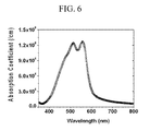
- FIG. 6 is a graph showing light absorption properties of a compound according to Synthesis Example 4,
- FIG. 7 is a graph showing external quantum efficiency according to a wavelength of an organic photoelectric device according to Example 1,
- FIG. 8 is a graph showing current density of the organic photoelectric device according to Example 1 according to a voltage
- FIG. 9 is a graph showing external quantum efficiency of an organic photoelectric device according to Example 2 according to a wavelength
- FIG. 10 is a graph showing current density of the organic photoelectric device according to Example 2 according to a voltage.
- substituted refers to one substituted with at least one substituent including a halogen (F, Br, Cl, or I), a hydroxy group, an alkoxy group, a nitro group, a cyano group, an amino group, an azido group, an amidino group, a hydrazino group, a hydrazono group, a carbonyl group, a carbamyl group, a thiol group, an ester group, a carboxyl group or a salt thereof, a sulfonic acid group or a salt thereof, a phosphoric acid group or a salt thereof, a C 1 to C 20 alkyl group, a C 2 to C 20 alkenyl group, a C 2 to C 20 alkynyl group, a C 6 to C 30 aryl group, a C 7 to C 30 arylalkyl group, a C 1 to C 4 alkoxy
- hetero may refer to one including 1 to 3 heteroatoms selected from N, O, S, and P.
- first”, “second”, etc. may be used herein to describe various elements, components, regions, layers and/or sections, these elements, components, regions, layers and/or sections are not to be limited by these terms. These terms are only used to distinguish one element, component, region, layer or section from another element, component, region, layer or section. Thus, a first element, component, region, layer or section discussed below could be termed a second element, component, region, layer or section without departing from the teachings of example embodiments.
- Example embodiments are described herein with reference to cross-sectional illustrations that are schematic illustrations of idealized embodiments (and intermediate structures) of example embodiments. As such, variations from the shapes of the illustrations as a result, for example, of manufacturing techniques and/or tolerances, are to be expected. Thus, example embodiments are not to be construed as limited to the particular shapes of regions illustrated herein but are to include deviations in shapes that result, for example, from manufacturing. For example, an implanted region illustrated as a rectangle may have rounded or curved features and/or a gradient of implant concentration at its edges rather than a binary change from implanted to non-implanted region.
- a buried region formed by implantation may result in some implantation in the region between the buried region and the surface through which the implantation takes place.
- the regions illustrated in the figures are schematic in nature and their shapes are not intended to illustrate the actual shape of a region of a device and are not intended to limit the scope of example embodiments.
- an organic photoelectric material may include a compound represented by the following Chemical Formula 1.
- A is a thiophene-containing aromatic group including 4 to 7 rings fused to each other, the A may include at least two thiophenes and at least one of the rings may include a heteroatom, and the heteroatom may include nitrogen (N), silicon (Si), oxygen (O), selenium (Se), or a combination thereof.
- the compound may have a thiophene-containing aromatic group including 4 to 7 rings at the core, and selectively absorbs light of a green wavelength region.
- the 4 to 7 rings are all fused together and thus may decrease conformational torsion of the compound and increase light absorption in a narrow wavelength region, that is, sharply in a wavelength region ranging from about 500 nm to about 600 nm, without dispersing the absorption wavelength region.
- the compound has a dicyanovinyl group as an electron acceptor at both ends thereof, and thus may increase a LUMO level, decrease a HOMO level and resultantly decrease a band gap.
- the compound may have a band gap ranging from about 2.0 eV to 3.0 eV. Accordingly, the compound may effectively absorb light of a wavelength region ranging from about 500 nm to 600 nm by adjusting its energy level and thus may have high external quantum efficiency (EQE) and improved photoelectric conversion efficiency.
- EQE external quantum efficiency
- the organic photoelectric material may, for example, include at least one of the compounds represented by the following Chemical Formulae 2 to 7.
- X 1 to X 5 are the same or different and are independently CR 1 R 2 , SiR 3 R 4 , NR 5 , oxygen (O), or selenium (Se), wherein R 1 to R 5 are the same or different and are independently hydrogen, a substituted or unsubstituted C 1 to C 20 alkyl group, a substituted or unsubstituted C 6 to C 20 aryl group, a substituted or unsubstituted C 3 to C 20 heteroaryl group, or a combination thereof.
- FIG. 1 is a cross-sectional view showing an organic photoelectric device according to example embodiments.
- an organic photoelectric device may include a first electrode (e.g., an anode) 10 and a second electrode (e.g., a cathode) 20 , and an active layer 30 interposed between the first electrode 10 and the second electrode 20 .
- the first electrode 10 is positioned under the active layer 30
- the second electrode 20 is positioned on the active layer 30
- the second electrode 20 may be positioned under the active layer 30 and the first electrode 10 may be positioned on the active layer 30 in an opposite way.
- Either one of the first electrode 10 and second electrode 20 may be made of, for example, a transparent conductor, e.g., indium tin oxide (ITO), indium zinc oxide (IZO), aluminum-doped zinc oxide (AZO), and gallium-doped zinc oxide (GZO), while the other may be made of, for example, an opaque conductor, e.g., aluminum (Al), copper (Cu), titanium (Ti), gold (Au), silver (Ag), chromium (Cr), titanium (Ti), an alloy thereof, or a combination thereof.
- a transparent conductor e.g., indium tin oxide (ITO), indium zinc oxide (IZO), aluminum-doped zinc oxide (AZO), and gallium-doped zinc oxide (GZO
- an opaque conductor e.g., aluminum (Al), copper (Cu), titanium (Ti), gold (Au), silver (Ag), chromium (Cr), titanium (Ti), an alloy thereof, or
- the active layer 30 may transform light into an electrical signal by using photoelectric effects, and includes the aforementioned organic photoelectric material.
- the active layer 30 includes the aforementioned organic photoelectric material, and may selectively absorb light of a green wavelength region and have a maximum absorption peak in a wavelength region of about 500 nm to about 600 nm in the absorption spectrum.
- the active layer 30 has a relatively small band gap ranging from about 2.0 eV to 3.0 eV as aforementioned, and may effectively absorb light in the wavelength region.
- the organic photoelectric material may be included in a p payer, an i layer, an n layer, or a combination thereof.
- the p layer may be formed to be adjacent to the first electrode 10
- the n layer may be formed to neighbor the second electrode 20
- the i layer may be formed to be adjacent to the p layer and the n layer.
- example embodiments are not limited thereto, and the i layer may be formed to be adjacent to the first electrode 10 and the second electrode 20 when the p layer and the n layer are not formed.
- the organic photoelectric material may be included in the p payer, the i layer, the n layer, or a combination thereof.
- the p layer includes a p-type material, and holes separated from excitons produced in the i layer are delivered thereto.
- the n layer includes an n-type material, and electrons separated from excitons produced from the i layer are delivered thereto.
- the i layer includes both of p-type and n-type materials and forms a pn junction, and also externally receives light, produces excitons, and separates the excitons into holes and electrons.
- a material having a lower LUMO level than the compound may be used as an n-type material.
- the compound may be included in the p layer, the i layer, or a combination thereof.
- the n-type material may be included in the n layer, the i layer, or a combination thereof.
- a compound represented by the above Chemical Formula 1 when a compound represented by the above Chemical Formula 1 may be used as an n-type material, a material having a higher LUMO level than the compound may be used as a p-type material.
- the compound may be included in the n layer, the i layer, or a combination thereof, and the p-type material may be included in the p layer, the i layer, or a combination thereof.
- the i layer may include a bulk heterojunction (BHJ), an organic/inorganic hybrid, or a combination thereof, without limitation.
- BHJ bulk heterojunction
- organic/inorganic hybrid organic/inorganic hybrid
- the bulk heterojunction may include at least two selected from a compound represented by the above Chemical Formula 1, polyaniline, polypyrrole, polythiophene, poly(p-phenylene vinylene), MEH-PPV (poly[2-methoxy-5-(2′-ethyl-hexyloxy)-1,4-phenylene vinylene), MDMO-PPV (poly(2-methoxy-5-(3,7-dimethyloctyloxy)-1,4-phenylene-vinylene)), pentacene, PEDOT (poly(3,4-ethylene dioxythiophene)), poly(3-allylthiophene), phthalocyanine, triarylamine, benzidine, pyrazoline, styrylamine, hydrazone, carbazole, thiophene, pyrrole, phenanthrene, tetracene, naphthalene, fullerene (C60, C70, C74, C76, C78, C
- the organic/inorganic hybrid layer may include an organic material selected from the compound represented by the above Chemical Formula 1, polyaniline, polypyrrole, polythiophene, poly(p-phenylene vinylene), MEH-PPV (poly[2-methoxy-5-(2′-ethyl-hexyloxy)-1,4-phenylene]vinylene), MDMO-PPV (poly(2-methoxy-5-(3,7-dimethyloctyloxy)-1,4-phenylene-vinylene)), pentacene, PEDOT (poly(3,4-ethylene dioxythiophene)), poly(3-alkylthiophene), phthalocyanine, triarylamine, bezidine, pyrazoline, styrylamine, hydrazone, carbazole, thiophene, pyrrole, phenanthrene, tetracene, naphthalene, fullerene (C60, C70, C74, C76,
- the p-type material for the i layer may be used for the p layer, while the n-type material for the i layer may be used for the n layer.
- the p-type material used for the i layer may be different from the material for the p layer, while the n-type material used for the i layer may be different from the material for the n layer.
- the active layer 30 may have a thickness of about 1 nm to about 500 nm. When the active layer 30 has a thickness within the range, the active layer 30 may effectively absorb light, more easily separate holes from electrons, and more easily transfer the separated holes and electrons, and thus improve photoelectric conversion efficiency.
- the active layer 30 may have a thickness ranging from about 5 nm to 300 nm within the range, for example, a thickness ranging from about 10 nm to 200 nm within the range.
- the organic photoelectric device produces excitons when the active layer 30 absorbs light of a green wavelength region entering from the first electrode 10 and/or the second electrode 20 .
- the excitons are separated into holes and electrons in the active layer 30 .
- the separated holes move toward the first electrode 10 while the electrons move toward the second electrode 20 , thereby forming a current in the organic photoelectric device.
- an auxiliary layer (not shown) is further included between the first electrode 10 and the active layer 30 and/or between the second electrode 20 and the active layer 30 in order to more easily move the holes and electrons separated in the active layer 30 .
- the auxiliary layer may include one selected from a hole transport layer (HTL), an electron blocking layer (EBL), an electron transport layer (ETL), and a hole blocking layer (HBL).
- HTL hole transport layer
- EBL electron blocking layer
- ETL electron transport layer
- HBL hole blocking layer
- the hole transport layer may play a role of facilitating transportation of holes, and may include one selected from, for example, PEDOT:PSS (poly(3,4-ethylene dioxythiophene):poly(styrene sulfonate)), polyarylamine, poly(N-vinylcarbazole), polyaniline, polypyrrole, TPD (N,N,N′,N′-tetrakis(4-methoxyphenyl)-benzidine), ⁇ -NPD (4-bis[N-(1-naphthyl)-N-phenyl-amino]piphenyl), m-MTDATA, TCTA (4,4′,4′′-tris(N-carbazolyl)-triphenylamine), and a combination thereof, without limitation.
- PEDOT:PSS poly(3,4-ethylene dioxythiophene):poly(styrene sulfonate)
- polyarylamine poly(N-vinylc
- the electron blocking layer (EBL) may play a role of prohibiting transportation of electrons and may include one selected from, for example, PEDOT:PSS (poly(3,4-ethylene dioxythiophene):poly(styrene sulfonate)), polyarylamine, poly(N-vinylcarbazole), polyaniline, polypyrrole, TPD (N,N,N′,N′-tetrakis(4-methoxyphenyl)-benzidine), ⁇ -NPD (4-bis[N-(1-naphthyl)-N-phenyl-amino]piphenyl), m-MTDATA, TCTA (4,4′,4′′-tris(N-carbazolyl)-triphenylamine), and a combination thereof, without limitation.
- PEDOT:PSS poly(3,4-ethylene dioxythiophene):poly(styrene sulfonate)
- polyarylamine poly(N-
- the electron transport layer may play a role of facilitating transportation of electrons, and may include one selected from, for example, NTCDA (1,4,5,8-naphthalene-tetracarboxylic dianhydride), BCP (bathocuproine), LiF, Alq 3 , Gaq 3 , Inq 3 , Znq 2 , Zn(BTZ) 2 , BeBq 2 , and a combination thereof, without limitation.
- the hole blocking layer may play a role of prohibiting transportation of holes, and may include one selected from NTCDA (1,4,5,8-naphthalene-tetracarboxylic dianhydride), BCP (bathocuproine), Li F, Alq 3 , Gaq 3 , Inq 3 , Znq 2 , Zn(BTZ) 2 , BeBq 2 , and a combination thereof, without limitation.
- the organic photoelectric device may be applied to various fields, for example a solar cell, an image sensor, a photo-detector, a photo-sensor, and an organic light emitting diode (OLED). Particularly, when the organic photoelectric device is applied to an image sensor, the organic photoelectric device may simultaneously replace a color filter and thus contribute to higher integration.
- a solar cell for example a solar cell, an image sensor, a photo-detector, a photo-sensor, and an organic light emitting diode (OLED).
- OLED organic light emitting diode
- the image sensor includes a pixel array in which a plurality of pixels are arranged in a matrix format, and each pixel may include the aforementioned organic photoelectric device.
- the organic photoelectric device may sense light and transfer the sensed information to a transistor.
- the resulting reaction mixture is extracted with 500 ml of methylene chloride (MC) (4 ⁇ ), dried using MgSO 4 , and then filtered through celite. Then, column chromatography (elution: a mixture of hexane and ethylacetate) is used to remove impurities from the reactant, obtaining 20.4 g of a yellow solid, and obtaining the following compound A.
- the compound has a yield of 60%.
- the sticky solid is dissolved in a mixed solvent of 400 ml of ether and 100 ml of THF and dried using MgSO 4 .
- the dried reactant is filtered, obtaining 16 g of a yellow solid having the following compound B.
- the compound has a yield of 93%.
- the blue solid is cleaned with 500 ml of 2 N HCl, 500 ml of H 2 O, and 500 ml of acetone and dried in an environment exposed to air, obtaining 14 g of a blue solid having the following compound D.
- the compound has a yield of 98%.
- the reaction mixture is cooled down in an ice bath, and 30 ml of NH 4 OH is added thereto. The mixture is stirred for 15 minutes. Then, 500 ml of water is added to the reaction mixture, and the resulting mixture is extracted with 300 ml of ether and 300 ml of methylene chloride. The extract is dried with MgSO 4 , filtered, and concentrated, obtaining a black residue. The black residue is dissolved in 200 ml of methylene chloride, and the solution is filtered using column chromatography (eluting solution: hexane), obtaining 6 g of a brownish yellow solid, the following compound F. The compound has a yield of 86%.
- a methylene chloride layer is separated from the reactant, and the remaining water layer is extracted with 200 ml of methylene chloride, dried using MgSO 4 , and then filtered and concentrated. The resulting product is then filtered using column chromatography (eluting solution: hexane, ethylacetate, and methylene chloride), obtaining 6.2 g of a yellow-orange solid. The compound has a yield of 88%.
- the mixture is extracted with 500 ml of methylene chloride, and the extract is dried with MgSO 4 . Then, the resulting product is filtered using column chromatography (eluting solution: hexane and ethylacetate), obtaining 3.22 g of a red solid, a compound H represented by Chemical Formula 6A. The compound has a yield of 43%.
- the compound H (Chemical Formula 6A) has NMR (400 MHz, DMSO-d6) data as follows.
- a compound represented by the following Chemical Formula 8 is prepared.
- the compounds according to Synthesis Examples 1 to 6 have a band gap ranging from about 2.0 to 3.0 eV, for example, about 2.0 to 2.7 eV.
- the compounds according to Synthesis Examples 1 to 6 are evaluated regarding light absorption properties according to wavelength.
- FIG. 2 is a graph showing extinction coefficients according to wavelengths of the compounds according to Synthesis Examples 1 to 3
- FIG. 3 is a graph showing extinction coefficients according to wavelengths of the compounds according to Synthesis Examples 4 to 6
- FIG. 4 is a graph showing extinction coefficients according to wavelengths of the compound according to Comparative Synthesis Example 1
- FIG. 5 is a graph showing extinction coefficients according to wavelengths of the compound according to Comparative Synthesis Example 2.
- the compounds according to Synthesis Examples 1 to 6 have a maximum absorption peak in a wavelength region ranging from about 500 nm to 600 nm, and thus selectively absorb light in a green wavelength region.
- the compounds have a sharp peak in the wavelength region and thus may improve sensitivity and color purity.
- the compound according to Comparative Synthesis Example 1 has a maximum absorption peak of less than about 500 nm but smaller absorption in a wavelength region ranging from 500 nm to 600 nm. Accordingly, the compound according to Comparative Synthesis Example 1 mainly absorbs light in a short wavelength region compared with the compounds according to Synthesis Examples 1 to 6.
- the compound according to Comparative Synthesis Example 2 mainly absorbs light in a wavelength region ranging from about 300 nm to about 700 nm. Accordingly, the compound according to Comparative Synthesis Example 2 has deteriorated selectivity for light in a green wavelength region.
- the compounds according to Synthesis Example 1 to 6 have higher selectivity for absorbing light in a green wavelength region ranging from about 500 to 600 nm than the compounds according to Comparative Synthesis Examples 1 and 2.
- the compound according to Synthesis Example 4 is fabricated into a thin film and then evaluated regarding light absorption properties according to wavelength.
- the light absorption properties according to wavelength are evaluated by using the compound according to Synthesis Example 4 to form a 70 nm-thick thin film at a deposition speed of 1 A/s in a thermal evaporator.
- the light absorption properties are evaluated by radiating ultraviolet (UV)-visible ray (UV-Vis) using Cary 5000 UV spectroscopy (Varian Inc.).
- FIG. 6 is a graph showing light absorption properties of the compound according to Synthesis Example 4.
- a film formed of the compound according to Synthesis Example 4 has a maximum absorption peak in a wavelength region ranging from about 500 nm to 600 nm. Accordingly, the film selectively absorbs light in a green wavelength region.
- ITO is sputtered and laminated on a glass substrate to form an about 120 nm-thick anode, and 30 nm of MoO as a hole transport layer HTL is deposited thereon.
- N,N′-dimethyl quinacridone (NNQA) as a p-type semiconductor material is deposited thereon to form a 35 nm-thick p-type layer.
- the compound represented by Chemical Formula 6A according to Synthesis Example 4 as an n-type semiconductor material is thermally deposited to be a 35 nm-thick n-type layer.
- aluminum (Al) is sputtered and laminated to fabricate an 80 nm-thick cathode, which is used to fabricate an organic photoelectric device.
- the organic photoelectric device according to Example 1 is evaluated regarding external quantum efficiency (EQE) according to wavelength.
- EQE external quantum efficiency
- the external quantum efficiency is measured using an IPCE measurement system (McScience Inc., Korea). First, a Si photodiode (Hamamatsu, Japan) is used to calibrate the equipment, and the organic photoelectric device according to Example 1 is mounted on the equipment and then measured regarding external quantum efficiency in a wavelength region ranging from 350-750 nm.
- FIG. 7 is a graph showing external quantum efficiency according to a wavelength of the organic photoelectric device according to Example 1.
- the organic photoelectric device according to Example 1 has a maximum peak of external quantum efficiency (EQE) in a green wavelength region ranging from about 500 nm to 600 nm, and in particular, about 27% external quantum efficiency (EQE) at a green wavelength region of 550 nm.
- EQE external quantum efficiency
- the organic photoelectric device according to Example 1 is measured regarding current density while various biases are applied thereto.
- FIG. 8 is a graph showing current density according to voltage of the organic photoelectric device according to Example 1.
- the organic photoelectric device according to Example 1 has a diode characteristic such that current flow is suppressed in a reverse voltage direction.
- An about 120 nm-thick anode is fabricated by sputtering and laminating ITO on a glass substrate, and 30 nm of MoO as a hole transport layer HTL is deposited thereon.
- a 90 nm-thick active layer is formed thereon by codepositing a mixture prepared by mixing dimethyl quinacridone (NNQA) as a p-type semiconductor material and a compound represented by the above Chemical Formula 6A in a composition ratio of 2:1.
- NQA dimethyl quinacridone
- Al aluminum
- the organic photoelectric device according to Example 2 is evaluated regarding external quantum efficiency (EQE) according to wavelength.
- EQE external quantum efficiency
- the external quantum efficiency is measured using an IPCE measurement system (McScience Inc., Korea). First, a Si photodiode (Hamamatsu, Japan) is used to calibrate equipment, and the organic photoelectric device according to Example 2 is mounted on the equipment. The organic photoelectric device is measured regarding external quantum efficiency in a wavelength region ranging from 350-750 nm.
- FIG. 9 is a graph showing external quantum efficiency according to a wavelength of the organic photoelectric device according to Example 2.
- the organic photoelectric device according to Example 2 has a maximum peak of external quantum efficiency (EQE) in a green wavelength region ranging from about 500 to 600 nm, for example, external quantum efficiency (EQE) of 20.6% at a wavelength of about 550 nm.
- EQE external quantum efficiency
- the organic photoelectric device according to Example 2 has external quantum efficiency that is changed as various voltages are applied thereto.
- the organic photoelectric device according to Example 2 is a sensor selectively absorbing green light in a visible ray region and generating a current, and thus amplifies a fine signal difference by applying a voltage thereto.
- the organic photoelectric device according to Example 2 has about 65.7% amplified efficiency without changing an external quantum efficiency graph when a voltage of ⁇ 5 V is applied thereto, for example, about 55% efficiency when a low voltage of ⁇ 3 V is applied thereto.
- the organic photoelectric device according to Example 2 is measured regarding current density while various biases are applied thereto.
- FIG. 10 is a graph showing a current density according to a voltage of the organic photoelectric device according to Example 2.
- the organic photoelectric device according to Example 2 has diode characteristic that suppress a current flow in a reverse voltage direction.
Landscapes
- Chemical & Material Sciences (AREA)
- Organic Chemistry (AREA)
- Physics & Mathematics (AREA)
- Engineering & Computer Science (AREA)
- Materials Engineering (AREA)
- Spectroscopy & Molecular Physics (AREA)
- Electromagnetism (AREA)
- Light Receiving Elements (AREA)
- Photovoltaic Devices (AREA)
- Electroluminescent Light Sources (AREA)
- Heterocyclic Carbon Compounds Containing A Hetero Ring Having Oxygen Or Sulfur (AREA)
- Solid State Image Pick-Up Elements (AREA)
Applications Claiming Priority (2)
| Application Number | Priority Date | Filing Date | Title |
|---|---|---|---|
| KR1020120073981A KR101860084B1 (ko) | 2012-07-06 | 2012-07-06 | 유기 광전 재료, 상기 유기 광전 재료를 포함하는 유기 광전 소자 및 이미지 센서 |
| KR10-2012-0073981 | 2012-07-06 |
Publications (2)
| Publication Number | Publication Date |
|---|---|
| US20140008619A1 US20140008619A1 (en) | 2014-01-09 |
| US8890134B2 true US8890134B2 (en) | 2014-11-18 |
Family
ID=48745815
Family Applications (1)
| Application Number | Title | Priority Date | Filing Date |
|---|---|---|---|
| US13/930,445 Active US8890134B2 (en) | 2012-07-06 | 2013-06-28 | Organic photoelectric material and organic photoelectric device and image sensor |
Country Status (5)
| Country | Link |
|---|---|
| US (1) | US8890134B2 (de) |
| EP (1) | EP2696351B1 (de) |
| JP (1) | JP6204724B2 (de) |
| KR (1) | KR101860084B1 (de) |
| CN (1) | CN103524531B (de) |
Cited By (2)
| Publication number | Priority date | Publication date | Assignee | Title |
|---|---|---|---|---|
| US11401289B2 (en) | 2019-06-25 | 2022-08-02 | Samsung Electronics Co., Ltd. | Compound and photoelectric device, image sensor and electronic device including the same |
| US11895910B2 (en) | 2017-08-23 | 2024-02-06 | Canon Kabushiki Kaisha | Organic compound and photoelectric conversion element |
Families Citing this family (28)
| Publication number | Priority date | Publication date | Assignee | Title |
|---|---|---|---|---|
| KR102000719B1 (ko) | 2012-10-25 | 2019-07-19 | 삼성전자주식회사 | 유기 광전 소자 및 이미지 센서 |
| DE102013110693B4 (de) * | 2013-09-27 | 2024-04-25 | Heliatek Gmbh | Photoaktives, organisches Material für optoelektronische Bauelemente |
| EP2903047A1 (de) * | 2014-01-31 | 2015-08-05 | Ecole Polytechnique Fédérale de Lausanne (EPFL) | Lochtransportierendes und lichtabsorbierendes Material für Festkörpersolarzellen |
| CN105960714B (zh) | 2014-02-05 | 2018-02-09 | 东丽株式会社 | 光电转换元件及图像传感器 |
| KR102282495B1 (ko) | 2014-07-21 | 2021-07-27 | 삼성전자주식회사 | 화합물, 유기 광전자 소자 및 이미지 센서 |
| JP6610257B2 (ja) | 2014-08-20 | 2019-11-27 | 東レ株式会社 | 光電変換素子ならびにそれを用いたイメージセンサ、太陽電池、単色検知センサおよびフレキシブルセンサ |
| JP2016063084A (ja) * | 2014-09-18 | 2016-04-25 | 株式会社東芝 | 有機光電変換素子及びこれを備える撮像装置 |
| JP6076302B2 (ja) * | 2014-09-22 | 2017-02-08 | 株式会社東芝 | 光電変換素子 |
| KR102282218B1 (ko) | 2015-01-30 | 2021-07-26 | 삼성전자주식회사 | 3 차원 영상 획득 장치용 결상 광학계 및 이를 포함하는 3 차원 영상 획득 장치 |
| KR102491494B1 (ko) | 2015-09-25 | 2023-01-20 | 삼성전자주식회사 | 유기 광전 소자용 화합물 및 이를 포함하는 유기 광전 소자 및 이미지 센서 |
| KR102529631B1 (ko) | 2015-11-30 | 2023-05-04 | 삼성전자주식회사 | 유기 광전 소자 및 이미지 센서 |
| KR102557864B1 (ko) | 2016-04-06 | 2023-07-19 | 삼성전자주식회사 | 화합물, 및 이를 포함하는 유기 광전 소자, 이미지 센서 및 전자 장치 |
| US10056563B2 (en) * | 2016-04-08 | 2018-08-21 | Samsung Electronics Co., Ltd. | Synthetic method of fused heteroaromatic compound and fused heteroaromatic compound, and intermediate thereof |
| US10236461B2 (en) * | 2016-05-20 | 2019-03-19 | Samsung Electronics Co., Ltd. | Organic photoelectronic device and image sensor |
| JP7433741B2 (ja) * | 2016-05-31 | 2024-02-20 | キヤノン株式会社 | 光電変換素子、二次元センサ、画像センサおよび撮像装置 |
| KR102605375B1 (ko) | 2016-06-29 | 2023-11-22 | 삼성전자주식회사 | 유기 광전 소자 및 이미지 센서 |
| KR102589215B1 (ko) | 2016-08-29 | 2023-10-12 | 삼성전자주식회사 | 유기 광전 소자, 이미지 센서 및 전자 장치 |
| CN106543200A (zh) * | 2016-11-01 | 2017-03-29 | 西安近代化学研究所 | 基于二苯并五元芳杂稠环a‑d‑a型共轭分子及其制备方法 |
| CN106810531A (zh) * | 2016-12-19 | 2017-06-09 | 西安近代化学研究所 | 基于茚并芴九并稠环a‑d‑a型共轭分子及其制备方法 |
| CN106831815B (zh) * | 2017-01-19 | 2019-06-28 | 湘潭大学 | 一种含噻吩并咔唑类七元稠环的a–d–a型有机小分子受体及其制备方法 |
| CN107573722B (zh) * | 2017-08-03 | 2019-06-28 | 湘潭大学 | 一种含二噻吩环戊咔唑的D–A–π–A型有机光敏化染料及其制备方法与应用 |
| KR102250385B1 (ko) * | 2017-10-18 | 2021-05-11 | 주식회사 엘지화학 | 유기 광 다이오드 및 이를 포함하는 유기 이미지 센서 |
| US11145822B2 (en) | 2017-10-20 | 2021-10-12 | Samsung Electronics Co., Ltd. | Compound and photoelectric device, image sensor, and electronic device including the same |
| CN111418079B (zh) * | 2018-01-10 | 2023-05-16 | 香港科技大学 | 基于稠环噻吩的芳香体系 |
| CN108299449B (zh) * | 2018-01-15 | 2020-08-25 | 华南协同创新研究院 | 一类基于咔唑并五元杂环单元的电致发光材料及其制备方法与应用 |
| WO2019161748A1 (en) * | 2018-02-23 | 2019-08-29 | Peking University | Organic semiconducting compounds |
| CN114591349B (zh) * | 2022-03-07 | 2023-04-07 | 中国科学院上海微系统与信息技术研究所 | 一种荧光化合物、其应用及三甲胺气体的检测方法 |
| WO2026063160A1 (ja) * | 2024-09-20 | 2026-03-26 | 富士フイルム株式会社 | 光電変換素子、撮像素子、光センサ、撮像素子の製造方法、化合物 |
Citations (16)
| Publication number | Priority date | Publication date | Assignee | Title |
|---|---|---|---|---|
| WO1999012989A1 (en) | 1997-09-05 | 1999-03-18 | Cambridge Display Technology Ltd. | Compounds for electronic devices |
| EP1279691A1 (de) | 2001-07-25 | 2003-01-29 | MERCK PATENT GmbH | Mono-, Oligo- und Polydifluorovinyl-(hetero)arylene, ihre Herstellung und Verwendng als Ladungstransportmaterial |
| WO2010020329A1 (en) | 2008-08-18 | 2010-02-25 | Merck Patent Gmbh, | Indacenodithiophene and indacenodiselenophene polymers and their use as organic semiconductors |
| US20100053387A1 (en) | 2008-08-26 | 2010-03-04 | Kim Gi-Bum | Image sensor with multiple types of color filters |
| JP2010083785A (ja) | 2008-09-30 | 2010-04-15 | Chisso Corp | 平面性の高い分子構造を有する化合物およびこれを用いた有機トランジスタ |
| JP2010093785A (ja) | 2008-09-10 | 2010-04-22 | Ntt Docomo Inc | べき級数型プリディストータ、べき級数型プリディストータの制御方法 |
| US20100168444A1 (en) | 2008-12-29 | 2010-07-01 | Eternal Chemical Co., Ltd. | Diindenothiophene derivatives and use thereof |
| CN101798310A (zh) | 2010-03-05 | 2010-08-11 | 中国科学院长春应用化学研究所 | 一种有机半导体材料及使用该材料的有机薄膜晶体管 |
| US20100305288A1 (en) | 2009-05-28 | 2010-12-02 | Mingqian He | Fused Thiophenes, Articles, and Methods Thereof |
| DE102009036110A1 (de) | 2009-06-05 | 2010-12-09 | Heliatek Gmbh | Licht absorbierendes organisches Bauelement |
| KR20100136931A (ko) | 2009-06-19 | 2010-12-29 | 주식회사 동진쎄미켐 | 신규한 유기염료 및 이의 제조방법 |
| JP2011029219A (ja) | 2009-07-21 | 2011-02-10 | Idemitsu Kosan Co Ltd | 有機薄膜太陽電池用材料及びそれを用いた有機薄膜太陽電池 |
| JP2011029220A (ja) | 2009-07-21 | 2011-02-10 | Idemitsu Kosan Co Ltd | 有機薄膜太陽電池用材料及びそれを用いた有機薄膜太陽電池 |
| EP2400575A1 (de) | 2010-06-24 | 2011-12-28 | heliatek GmbH | Optoelektronisches Bauelement mit organischen Schichten |
| WO2011161262A1 (de) | 2010-06-24 | 2011-12-29 | Heliatek Gmbh | Verdampfbares organisch halbleitendes material und dessen verwendung in einem optoelektronischen bauelement |
| JP2012036180A (ja) | 2010-07-13 | 2012-02-23 | Sumitomo Chemical Co Ltd | 縮合環化合物の製造方法、および該方法に用いられる原料化合物 |
Family Cites Families (2)
| Publication number | Priority date | Publication date | Assignee | Title |
|---|---|---|---|---|
| ATE303389T1 (de) * | 2001-07-09 | 2005-09-15 | Merck Patent Gmbh | Thienothiophen-derivate |
| CN101139317B (zh) * | 2007-05-15 | 2011-09-07 | 南京邮电大学 | 含咔唑单元的有机半导体材料及合成 |
-
2012
- 2012-07-06 KR KR1020120073981A patent/KR101860084B1/ko active Active
-
2013
- 2013-06-28 US US13/930,445 patent/US8890134B2/en active Active
- 2013-07-05 EP EP13175391.5A patent/EP2696351B1/de active Active
- 2013-07-05 JP JP2013141757A patent/JP6204724B2/ja active Active
- 2013-07-08 CN CN201310283609.XA patent/CN103524531B/zh active Active
Patent Citations (19)
| Publication number | Priority date | Publication date | Assignee | Title |
|---|---|---|---|---|
| WO1999012989A1 (en) | 1997-09-05 | 1999-03-18 | Cambridge Display Technology Ltd. | Compounds for electronic devices |
| EP1279691A1 (de) | 2001-07-25 | 2003-01-29 | MERCK PATENT GmbH | Mono-, Oligo- und Polydifluorovinyl-(hetero)arylene, ihre Herstellung und Verwendng als Ladungstransportmaterial |
| WO2010020329A1 (en) | 2008-08-18 | 2010-02-25 | Merck Patent Gmbh, | Indacenodithiophene and indacenodiselenophene polymers and their use as organic semiconductors |
| US20100053387A1 (en) | 2008-08-26 | 2010-03-04 | Kim Gi-Bum | Image sensor with multiple types of color filters |
| JP2010093785A (ja) | 2008-09-10 | 2010-04-22 | Ntt Docomo Inc | べき級数型プリディストータ、べき級数型プリディストータの制御方法 |
| JP2010083785A (ja) | 2008-09-30 | 2010-04-15 | Chisso Corp | 平面性の高い分子構造を有する化合物およびこれを用いた有機トランジスタ |
| US20100168444A1 (en) | 2008-12-29 | 2010-07-01 | Eternal Chemical Co., Ltd. | Diindenothiophene derivatives and use thereof |
| US20100305288A1 (en) | 2009-05-28 | 2010-12-02 | Mingqian He | Fused Thiophenes, Articles, and Methods Thereof |
| DE102009036110A1 (de) | 2009-06-05 | 2010-12-09 | Heliatek Gmbh | Licht absorbierendes organisches Bauelement |
| KR20100136931A (ko) | 2009-06-19 | 2010-12-29 | 주식회사 동진쎄미켐 | 신규한 유기염료 및 이의 제조방법 |
| JP2011029219A (ja) | 2009-07-21 | 2011-02-10 | Idemitsu Kosan Co Ltd | 有機薄膜太陽電池用材料及びそれを用いた有機薄膜太陽電池 |
| JP2011029220A (ja) | 2009-07-21 | 2011-02-10 | Idemitsu Kosan Co Ltd | 有機薄膜太陽電池用材料及びそれを用いた有機薄膜太陽電池 |
| CN101798310A (zh) | 2010-03-05 | 2010-08-11 | 中国科学院长春应用化学研究所 | 一种有机半导体材料及使用该材料的有机薄膜晶体管 |
| EP2400575A1 (de) | 2010-06-24 | 2011-12-28 | heliatek GmbH | Optoelektronisches Bauelement mit organischen Schichten |
| WO2011161170A1 (de) | 2010-06-24 | 2011-12-29 | Heliatek Gmbh | Optoelektronisches bauelement mit organischen schichten |
| WO2011161262A1 (de) | 2010-06-24 | 2011-12-29 | Heliatek Gmbh | Verdampfbares organisch halbleitendes material und dessen verwendung in einem optoelektronischen bauelement |
| US20130167930A1 (en) | 2010-06-24 | 2013-07-04 | Heliatek Gmbh | Evaporable organic semiconductive material and use thereof in an optoelectronic component |
| US20130167931A1 (en) | 2010-06-24 | 2013-07-04 | Dirk Hildebrandt | Optoelectronic component with organic layers |
| JP2012036180A (ja) | 2010-07-13 | 2012-02-23 | Sumitomo Chemical Co Ltd | 縮合環化合物の製造方法、および該方法に用いられる原料化合物 |
Non-Patent Citations (19)
| Title |
|---|
| Ali Yassin, Evaluation of Bis-Dicyanovinyl Short-Chain Conjugated Systems As Donor Materials for Organic Solar Cells, Solar Energy Materials & Solar Cells, 2010 Elsevier B.V., pp. 462-468. |
| C. Tseng et al. "A pentacyclic Nitrogen-Bridged Thienyi-Phenylene-Thienyl Arene for Donor-Acceptor Copolymers: Synthesis, Characterization, and Applications in Field-Effect Transistors and Polymer Solar Cells"; Chemistry-An Asian Journal, vol. 7, pp. 2102-10, 2012; XP0055121926. |
| European Search Report dated Jun. 18, 2014 for corresponding application No. 13 175 391.5. |
| K. Xiao et al. "A highly p-stacked organic semiconductor for field-effect transistors based on linearly condensed pentathienoacene"; Journal of the American Chemical Society, vol. 127, pp. 13281-13286, 2005; XP55122393. |
| Kazuo Takimiya, Thienoacene-based Organic Semiconductors, 2011 Wiley-VCH Verlag GmbH & Co., Advanced Materials, pp. 1-24. |
| M. Jørgensen et al. "Easy Access to 3,8-Diaryldifurano[2,3-a:2',3'-f]naphthalenes. A New Extended Aromatic System"; Journal of Organic Chemistry, vol. 65, pp. 8783-8785, 2000; XP0055006875. |
| Raja Shahid Ashraf, Silaindacenodithiophene Semiconducting Polymers for Efficient Solar Cells and High-Mobility Ambipolar Transistors, 2010 American Chemical Society, pp. 768-770. |
| Ravi Kumar Cheedarala, Ladder-Type Heteroacene Polymers Bearing Carbazole and Thiophene Ring Units and Their Use in Field-Effect Transistors and Photovoltaic Cells, Journal of Materials Chemistry, The Royal Society of Chemistry 2011, pp. 843-850. |
| Ted M. Pappenfus, Reduced Band Gap Dithieno[3,2-b:2',3'-d]Pyrroles: New N-Type Organic Materials Via Unexpected Reactivity, Organic Letters 2008, vol. 10, No. 8, pp. 1553-1556. |
| Ted M. Pappenfus, Reduced Band Gap Dithieno[3,2-b:2′,3′-d]Pyrroles: New N-Type Organic Materials Via Unexpected Reactivity, Organic Letters 2008, vol. 10, No. 8, pp. 1553-1556. |
| Weimin Zhang, Indacenodithiophene Semiconducting Polymers for High-Performance, Air-Stable Transistors, 2010 American Chemical Society, pp. 11437-11439. |
| X. Zhang et al. "Effect of Ring Fusion on the Electronic Absorption and Emission Properties of Oligothiophenes"; Journal of Organic Chemistry, vol. 68, pp. 9813-9815, 2003; XP002343472. |
| Xugeng Guo, Theoretical Investigations of the Structures and Electronic Spectra of 2-Dicyanovinyldithieno[2,3-b:,3',2'-d]Thiophene (DCST) and 2-Dicyanovinyldithieno[3,2-b:2',3'-d]Thiophene (DCTT), Journal of Molecular Structure: Theochem, 2009, pp. 179-184. |
| Xugeng Guo, Theoretical Investigations of the Structures and Electronic Spectra of 2-Dicyanovinyldithieno[2,3-b:,3′,2′-d]Thiophene (DCST) and 2-Dicyanovinyldithieno[3,2-b:2′,3′-d]Thiophene (DCTT), Journal of Molecular Structure: Theochem, 2009, pp. 179-184. |
| Y. Cheng et al. "Carbazole-Based ladder-Type Heptacylic Arene with Aliphatic Side Chains leading to Enhanced Efficiency of Organic Photovoltaics"; Chemistry of Materials, vol. 23, pp. 2361-2369, 2011; XP0055121925. |
| Y. Sun et al. "Chemically Doped and Cross-linked Hole-Transporting Materials as an Efficient Anode Buffer layer for Polymer Solar Cells"; Chemistry of Materials, vol. 23, pp. 5006-5015, 2011; XP0055121934. |
| Yen-Ju Cheng, Carbazole-based Ladder-Type Heptacylic Arene with Aliphatic Side Chains Leading to Enhanced Effiency of Organic Photovoltaics, 2011 American Chemical Society, pp. 2361-2369. |
| Zhang et al. "Synthesis and Structure of Fused alpha-Oligothiophenes with up to Seven Rings"; Journal of the American Chemical Society, vol. 127, pp. 10502-10503, 2005; XP008139244. |
| Zhang et al. "Synthesis and Structure of Fused α-Oligothiophenes with up to Seven Rings"; Journal of the American Chemical Society, vol. 127, pp. 10502-10503, 2005; XP008139244. |
Cited By (2)
| Publication number | Priority date | Publication date | Assignee | Title |
|---|---|---|---|---|
| US11895910B2 (en) | 2017-08-23 | 2024-02-06 | Canon Kabushiki Kaisha | Organic compound and photoelectric conversion element |
| US11401289B2 (en) | 2019-06-25 | 2022-08-02 | Samsung Electronics Co., Ltd. | Compound and photoelectric device, image sensor and electronic device including the same |
Also Published As
| Publication number | Publication date |
|---|---|
| CN103524531A (zh) | 2014-01-22 |
| JP2014017484A (ja) | 2014-01-30 |
| US20140008619A1 (en) | 2014-01-09 |
| EP2696351A3 (de) | 2014-07-16 |
| KR20140006597A (ko) | 2014-01-16 |
| JP6204724B2 (ja) | 2017-09-27 |
| KR101860084B1 (ko) | 2018-05-23 |
| CN103524531B (zh) | 2017-11-28 |
| EP2696351A2 (de) | 2014-02-12 |
| EP2696351B1 (de) | 2017-10-25 |
Similar Documents
| Publication | Publication Date | Title |
|---|---|---|
| US8890134B2 (en) | Organic photoelectric material and organic photoelectric device and image sensor | |
| US10566544B2 (en) | Compound and organic photoelectric device, image sensor and electronic device including the same | |
| EP3026722B1 (de) | Verbindung für organische fotoelektrische vorrichtung und bildsensor einer organischen fotoelektrischen vorrichtung sowie elektronische vorrichtung damit | |
| US9818956B2 (en) | Compound for organic photoelectric device and organic photoelectric device, image sensor, and electronic device including the same | |
| US10256414B2 (en) | Organic photoelectronic device and image sensor | |
| US9673259B2 (en) | Organic photoelectronic device and image sensor | |
| US8999526B2 (en) | Organic photoelectronic device and image sensor | |
| US9911920B2 (en) | Compound, organic photoelectronic device and image sensor | |
| US9887370B2 (en) | Compound for organic photoelectric device and organic photoelectric device image sensor, and electronic device including the same | |
| US9548463B2 (en) | Organic photoelectronic device and image sensor | |
| US9287509B2 (en) | Quinacridone derivative, and photoactive layer and photoelectric conversion device including same | |
| US9548336B2 (en) | Image sensors and electronic devices including the same | |
| US10181497B2 (en) | Optoelectronic device, and image sensor and electronic device including the same | |
| US10263042B2 (en) | Organic photoelectric device and image sensor | |
| US9786847B2 (en) | Compound for organic photoelectric device, and organic photoelectric device and image sensor including the same | |
| US9368727B2 (en) | Organic photoelectric device and image sensor including the same | |
| US10000462B2 (en) | Optoelectronic material and organic optoelectronic device and image sensor | |
| EP2975644A1 (de) | Verbindung, organische fotoelektronische vorrichtung und bildsensor |
Legal Events
| Date | Code | Title | Description |
|---|---|---|---|
| AS | Assignment |
Owner name: SAMSUNG ELECTRONICS CO., LTD., KOREA, REPUBLIC OF Free format text: ASSIGNMENT OF ASSIGNORS INTEREST;ASSIGNORS:LEE, KWANG HEE;KIM, KYU SIK;PARK, KYUNG BAE;AND OTHERS;REEL/FRAME:030711/0347 Effective date: 20130620 |
|
| STCF | Information on status: patent grant |
Free format text: PATENTED CASE |
|
| FEPP | Fee payment procedure |
Free format text: PAYOR NUMBER ASSIGNED (ORIGINAL EVENT CODE: ASPN); ENTITY STATUS OF PATENT OWNER: LARGE ENTITY |
|
| MAFP | Maintenance fee payment |
Free format text: PAYMENT OF MAINTENANCE FEE, 4TH YEAR, LARGE ENTITY (ORIGINAL EVENT CODE: M1551) Year of fee payment: 4 |
|
| MAFP | Maintenance fee payment |
Free format text: PAYMENT OF MAINTENANCE FEE, 8TH YEAR, LARGE ENTITY (ORIGINAL EVENT CODE: M1552); ENTITY STATUS OF PATENT OWNER: LARGE ENTITY Year of fee payment: 8 |