US8995041B2 - Ternary nickel oxide materials for electrochromic devices - Google Patents
Ternary nickel oxide materials for electrochromic devices Download PDFInfo
- Publication number
- US8995041B2 US8995041B2 US13/961,184 US201313961184A US8995041B2 US 8995041 B2 US8995041 B2 US 8995041B2 US 201313961184 A US201313961184 A US 201313961184A US 8995041 B2 US8995041 B2 US 8995041B2
- Authority
- US
- United States
- Prior art keywords
- ranges
- nizr
- electrochromic
- counter electrode
- oxide
- Prior art date
- Legal status (The legal status is an assumption and is not a legal conclusion. Google has not performed a legal analysis and makes no representation as to the accuracy of the status listed.)
- Active
Links
Images


Classifications
-
- G—PHYSICS
- G02—OPTICS
- G02F—OPTICAL DEVICES OR ARRANGEMENTS FOR THE CONTROL OF LIGHT BY MODIFICATION OF THE OPTICAL PROPERTIES OF THE MEDIA OF THE ELEMENTS INVOLVED THEREIN; NON-LINEAR OPTICS; FREQUENCY-CHANGING OF LIGHT; OPTICAL LOGIC ELEMENTS; OPTICAL ANALOGUE/DIGITAL CONVERTERS
- G02F1/00—Devices or arrangements for the control of the intensity, colour, phase, polarisation or direction of light arriving from an independent light source, e.g. switching, gating or modulating; Non-linear optics
- G02F1/01—Devices or arrangements for the control of the intensity, colour, phase, polarisation or direction of light arriving from an independent light source, e.g. switching, gating or modulating; Non-linear optics for the control of the intensity, phase, polarisation or colour
- G02F1/15—Devices or arrangements for the control of the intensity, colour, phase, polarisation or direction of light arriving from an independent light source, e.g. switching, gating or modulating; Non-linear optics for the control of the intensity, phase, polarisation or colour based on an electrochromic effect
-
- G—PHYSICS
- G02—OPTICS
- G02F—OPTICAL DEVICES OR ARRANGEMENTS FOR THE CONTROL OF LIGHT BY MODIFICATION OF THE OPTICAL PROPERTIES OF THE MEDIA OF THE ELEMENTS INVOLVED THEREIN; NON-LINEAR OPTICS; FREQUENCY-CHANGING OF LIGHT; OPTICAL LOGIC ELEMENTS; OPTICAL ANALOGUE/DIGITAL CONVERTERS
- G02F1/00—Devices or arrangements for the control of the intensity, colour, phase, polarisation or direction of light arriving from an independent light source, e.g. switching, gating or modulating; Non-linear optics
- G02F1/01—Devices or arrangements for the control of the intensity, colour, phase, polarisation or direction of light arriving from an independent light source, e.g. switching, gating or modulating; Non-linear optics for the control of the intensity, phase, polarisation or colour
- G02F1/15—Devices or arrangements for the control of the intensity, colour, phase, polarisation or direction of light arriving from an independent light source, e.g. switching, gating or modulating; Non-linear optics for the control of the intensity, phase, polarisation or colour based on an electrochromic effect
- G02F1/153—Constructional details
- G02F1/155—Electrodes
-
- C—CHEMISTRY; METALLURGY
- C23—COATING METALLIC MATERIAL; COATING MATERIAL WITH METALLIC MATERIAL; CHEMICAL SURFACE TREATMENT; DIFFUSION TREATMENT OF METALLIC MATERIAL; COATING BY VACUUM EVAPORATION, BY SPUTTERING, BY ION IMPLANTATION OR BY CHEMICAL VAPOUR DEPOSITION, IN GENERAL; INHIBITING CORROSION OF METALLIC MATERIAL OR INCRUSTATION IN GENERAL
- C23C—COATING METALLIC MATERIAL; COATING MATERIAL WITH METALLIC MATERIAL; SURFACE TREATMENT OF METALLIC MATERIAL BY DIFFUSION INTO THE SURFACE, BY CHEMICAL CONVERSION OR SUBSTITUTION; COATING BY VACUUM EVAPORATION, BY SPUTTERING, BY ION IMPLANTATION OR BY CHEMICAL VAPOUR DEPOSITION, IN GENERAL
- C23C14/00—Coating by vacuum evaporation, by sputtering or by ion implantation of the coating forming material
- C23C14/06—Coating by vacuum evaporation, by sputtering or by ion implantation of the coating forming material characterised by the coating material
- C23C14/08—Oxides
-
- C—CHEMISTRY; METALLURGY
- C23—COATING METALLIC MATERIAL; COATING MATERIAL WITH METALLIC MATERIAL; CHEMICAL SURFACE TREATMENT; DIFFUSION TREATMENT OF METALLIC MATERIAL; COATING BY VACUUM EVAPORATION, BY SPUTTERING, BY ION IMPLANTATION OR BY CHEMICAL VAPOUR DEPOSITION, IN GENERAL; INHIBITING CORROSION OF METALLIC MATERIAL OR INCRUSTATION IN GENERAL
- C23C—COATING METALLIC MATERIAL; COATING MATERIAL WITH METALLIC MATERIAL; SURFACE TREATMENT OF METALLIC MATERIAL BY DIFFUSION INTO THE SURFACE, BY CHEMICAL CONVERSION OR SUBSTITUTION; COATING BY VACUUM EVAPORATION, BY SPUTTERING, BY ION IMPLANTATION OR BY CHEMICAL VAPOUR DEPOSITION, IN GENERAL
- C23C14/00—Coating by vacuum evaporation, by sputtering or by ion implantation of the coating forming material
- C23C14/22—Coating by vacuum evaporation, by sputtering or by ion implantation of the coating forming material characterised by the process of coating
- C23C14/34—Sputtering
-
- C—CHEMISTRY; METALLURGY
- C23—COATING METALLIC MATERIAL; COATING MATERIAL WITH METALLIC MATERIAL; CHEMICAL SURFACE TREATMENT; DIFFUSION TREATMENT OF METALLIC MATERIAL; COATING BY VACUUM EVAPORATION, BY SPUTTERING, BY ION IMPLANTATION OR BY CHEMICAL VAPOUR DEPOSITION, IN GENERAL; INHIBITING CORROSION OF METALLIC MATERIAL OR INCRUSTATION IN GENERAL
- C23C—COATING METALLIC MATERIAL; COATING MATERIAL WITH METALLIC MATERIAL; SURFACE TREATMENT OF METALLIC MATERIAL BY DIFFUSION INTO THE SURFACE, BY CHEMICAL CONVERSION OR SUBSTITUTION; COATING BY VACUUM EVAPORATION, BY SPUTTERING, BY ION IMPLANTATION OR BY CHEMICAL VAPOUR DEPOSITION, IN GENERAL
- C23C14/00—Coating by vacuum evaporation, by sputtering or by ion implantation of the coating forming material
- C23C14/22—Coating by vacuum evaporation, by sputtering or by ion implantation of the coating forming material characterised by the process of coating
- C23C14/34—Sputtering
- C23C14/3407—Cathode assembly for sputtering apparatus, e.g. Target
- C23C14/3414—Metallurgical or chemical aspects of target preparation, e.g. casting, powder metallurgy
-
- C—CHEMISTRY; METALLURGY
- C23—COATING METALLIC MATERIAL; COATING MATERIAL WITH METALLIC MATERIAL; CHEMICAL SURFACE TREATMENT; DIFFUSION TREATMENT OF METALLIC MATERIAL; COATING BY VACUUM EVAPORATION, BY SPUTTERING, BY ION IMPLANTATION OR BY CHEMICAL VAPOUR DEPOSITION, IN GENERAL; INHIBITING CORROSION OF METALLIC MATERIAL OR INCRUSTATION IN GENERAL
- C23C—COATING METALLIC MATERIAL; COATING MATERIAL WITH METALLIC MATERIAL; SURFACE TREATMENT OF METALLIC MATERIAL BY DIFFUSION INTO THE SURFACE, BY CHEMICAL CONVERSION OR SUBSTITUTION; COATING BY VACUUM EVAPORATION, BY SPUTTERING, BY ION IMPLANTATION OR BY CHEMICAL VAPOUR DEPOSITION, IN GENERAL
- C23C14/00—Coating by vacuum evaporation, by sputtering or by ion implantation of the coating forming material
- C23C14/22—Coating by vacuum evaporation, by sputtering or by ion implantation of the coating forming material characterised by the process of coating
- C23C14/34—Sputtering
- C23C14/3464—Sputtering using more than one target
-
- G—PHYSICS
- G02—OPTICS
- G02F—OPTICAL DEVICES OR ARRANGEMENTS FOR THE CONTROL OF LIGHT BY MODIFICATION OF THE OPTICAL PROPERTIES OF THE MEDIA OF THE ELEMENTS INVOLVED THEREIN; NON-LINEAR OPTICS; FREQUENCY-CHANGING OF LIGHT; OPTICAL LOGIC ELEMENTS; OPTICAL ANALOGUE/DIGITAL CONVERTERS
- G02F1/00—Devices or arrangements for the control of the intensity, colour, phase, polarisation or direction of light arriving from an independent light source, e.g. switching, gating or modulating; Non-linear optics
- G02F1/01—Devices or arrangements for the control of the intensity, colour, phase, polarisation or direction of light arriving from an independent light source, e.g. switching, gating or modulating; Non-linear optics for the control of the intensity, phase, polarisation or colour
- G02F1/15—Devices or arrangements for the control of the intensity, colour, phase, polarisation or direction of light arriving from an independent light source, e.g. switching, gating or modulating; Non-linear optics for the control of the intensity, phase, polarisation or colour based on an electrochromic effect
- G02F1/1514—Devices or arrangements for the control of the intensity, colour, phase, polarisation or direction of light arriving from an independent light source, e.g. switching, gating or modulating; Non-linear optics for the control of the intensity, phase, polarisation or colour based on an electrochromic effect characterised by the electrochromic material, e.g. by the electrodeposited material
- G02F1/1523—Devices or arrangements for the control of the intensity, colour, phase, polarisation or direction of light arriving from an independent light source, e.g. switching, gating or modulating; Non-linear optics for the control of the intensity, phase, polarisation or colour based on an electrochromic effect characterised by the electrochromic material, e.g. by the electrodeposited material comprising inorganic material
-
- G—PHYSICS
- G02—OPTICS
- G02F—OPTICAL DEVICES OR ARRANGEMENTS FOR THE CONTROL OF LIGHT BY MODIFICATION OF THE OPTICAL PROPERTIES OF THE MEDIA OF THE ELEMENTS INVOLVED THEREIN; NON-LINEAR OPTICS; FREQUENCY-CHANGING OF LIGHT; OPTICAL LOGIC ELEMENTS; OPTICAL ANALOGUE/DIGITAL CONVERTERS
- G02F1/00—Devices or arrangements for the control of the intensity, colour, phase, polarisation or direction of light arriving from an independent light source, e.g. switching, gating or modulating; Non-linear optics
- G02F1/01—Devices or arrangements for the control of the intensity, colour, phase, polarisation or direction of light arriving from an independent light source, e.g. switching, gating or modulating; Non-linear optics for the control of the intensity, phase, polarisation or colour
- G02F1/15—Devices or arrangements for the control of the intensity, colour, phase, polarisation or direction of light arriving from an independent light source, e.g. switching, gating or modulating; Non-linear optics for the control of the intensity, phase, polarisation or colour based on an electrochromic effect
- G02F1/1514—Devices or arrangements for the control of the intensity, colour, phase, polarisation or direction of light arriving from an independent light source, e.g. switching, gating or modulating; Non-linear optics for the control of the intensity, phase, polarisation or colour based on an electrochromic effect characterised by the electrochromic material, e.g. by the electrodeposited material
- G02F1/1523—Devices or arrangements for the control of the intensity, colour, phase, polarisation or direction of light arriving from an independent light source, e.g. switching, gating or modulating; Non-linear optics for the control of the intensity, phase, polarisation or colour based on an electrochromic effect characterised by the electrochromic material, e.g. by the electrodeposited material comprising inorganic material
- G02F1/1524—Transition metal compounds
-
- H—ELECTRICITY
- H01—ELECTRIC ELEMENTS
- H01M—PROCESSES OR MEANS, e.g. BATTERIES, FOR THE DIRECT CONVERSION OF CHEMICAL ENERGY INTO ELECTRICAL ENERGY
- H01M14/00—Electrochemical current or voltage generators not provided for in groups H01M6/00 - H01M12/00; Manufacture thereof
- H01M14/005—Photoelectrochemical storage cells
-
- H—ELECTRICITY
- H01—ELECTRIC ELEMENTS
- H01M—PROCESSES OR MEANS, e.g. BATTERIES, FOR THE DIRECT CONVERSION OF CHEMICAL ENERGY INTO ELECTRICAL ENERGY
- H01M4/00—Electrodes
- H01M4/02—Electrodes composed of, or comprising, active material
- H01M4/04—Processes of manufacture in general
- H01M4/0402—Methods of deposition of the material
- H01M4/0421—Methods of deposition of the material involving vapour deposition
- H01M4/0423—Physical vapour deposition
- H01M4/0426—Sputtering
-
- H—ELECTRICITY
- H01—ELECTRIC ELEMENTS
- H01M—PROCESSES OR MEANS, e.g. BATTERIES, FOR THE DIRECT CONVERSION OF CHEMICAL ENERGY INTO ELECTRICAL ENERGY
- H01M4/00—Electrodes
- H01M4/02—Electrodes composed of, or comprising, active material
- H01M4/36—Selection of substances as active materials, active masses, active liquids
- H01M4/38—Selection of substances as active materials, active masses, active liquids of elements or alloys
- H01M4/381—Alkaline or alkaline earth metals elements
- H01M4/382—Lithium
-
- H—ELECTRICITY
- H01—ELECTRIC ELEMENTS
- H01M—PROCESSES OR MEANS, e.g. BATTERIES, FOR THE DIRECT CONVERSION OF CHEMICAL ENERGY INTO ELECTRICAL ENERGY
- H01M4/00—Electrodes
- H01M4/02—Electrodes composed of, or comprising, active material
- H01M4/36—Selection of substances as active materials, active masses, active liquids
- H01M4/48—Selection of substances as active materials, active masses, active liquids of inorganic oxides or hydroxides
-
- H—ELECTRICITY
- H01—ELECTRIC ELEMENTS
- H01M—PROCESSES OR MEANS, e.g. BATTERIES, FOR THE DIRECT CONVERSION OF CHEMICAL ENERGY INTO ELECTRICAL ENERGY
- H01M4/00—Electrodes
- H01M4/02—Electrodes composed of, or comprising, active material
- H01M4/36—Selection of substances as active materials, active masses, active liquids
- H01M4/48—Selection of substances as active materials, active masses, active liquids of inorganic oxides or hydroxides
- H01M4/50—Selection of substances as active materials, active masses, active liquids of inorganic oxides or hydroxides of manganese
- H01M4/505—Selection of substances as active materials, active masses, active liquids of inorganic oxides or hydroxides of manganese of mixed oxides or hydroxides containing manganese for inserting or intercalating light metals, e.g. LiMn2O4 or LiMn2OxFy
-
- H—ELECTRICITY
- H01—ELECTRIC ELEMENTS
- H01M—PROCESSES OR MEANS, e.g. BATTERIES, FOR THE DIRECT CONVERSION OF CHEMICAL ENERGY INTO ELECTRICAL ENERGY
- H01M4/00—Electrodes
- H01M4/02—Electrodes composed of, or comprising, active material
- H01M4/36—Selection of substances as active materials, active masses, active liquids
- H01M4/48—Selection of substances as active materials, active masses, active liquids of inorganic oxides or hydroxides
- H01M4/52—Selection of substances as active materials, active masses, active liquids of inorganic oxides or hydroxides of nickel, cobalt or iron
- H01M4/525—Selection of substances as active materials, active masses, active liquids of inorganic oxides or hydroxides of nickel, cobalt or iron of mixed oxides or hydroxides containing iron, cobalt or nickel for inserting or intercalating light metals, e.g. LiNiO2, LiCoO2 or LiCoOxFy
-
- G—PHYSICS
- G02—OPTICS
- G02F—OPTICAL DEVICES OR ARRANGEMENTS FOR THE CONTROL OF LIGHT BY MODIFICATION OF THE OPTICAL PROPERTIES OF THE MEDIA OF THE ELEMENTS INVOLVED THEREIN; NON-LINEAR OPTICS; FREQUENCY-CHANGING OF LIGHT; OPTICAL LOGIC ELEMENTS; OPTICAL ANALOGUE/DIGITAL CONVERTERS
- G02F1/00—Devices or arrangements for the control of the intensity, colour, phase, polarisation or direction of light arriving from an independent light source, e.g. switching, gating or modulating; Non-linear optics
- G02F1/01—Devices or arrangements for the control of the intensity, colour, phase, polarisation or direction of light arriving from an independent light source, e.g. switching, gating or modulating; Non-linear optics for the control of the intensity, phase, polarisation or colour
- G02F1/15—Devices or arrangements for the control of the intensity, colour, phase, polarisation or direction of light arriving from an independent light source, e.g. switching, gating or modulating; Non-linear optics for the control of the intensity, phase, polarisation or colour based on an electrochromic effect
- G02F2001/1502—Devices or arrangements for the control of the intensity, colour, phase, polarisation or direction of light arriving from an independent light source, e.g. switching, gating or modulating; Non-linear optics for the control of the intensity, phase, polarisation or colour based on an electrochromic effect complementary cell
-
- G—PHYSICS
- G02—OPTICS
- G02F—OPTICAL DEVICES OR ARRANGEMENTS FOR THE CONTROL OF LIGHT BY MODIFICATION OF THE OPTICAL PROPERTIES OF THE MEDIA OF THE ELEMENTS INVOLVED THEREIN; NON-LINEAR OPTICS; FREQUENCY-CHANGING OF LIGHT; OPTICAL LOGIC ELEMENTS; OPTICAL ANALOGUE/DIGITAL CONVERTERS
- G02F1/00—Devices or arrangements for the control of the intensity, colour, phase, polarisation or direction of light arriving from an independent light source, e.g. switching, gating or modulating; Non-linear optics
- G02F1/01—Devices or arrangements for the control of the intensity, colour, phase, polarisation or direction of light arriving from an independent light source, e.g. switching, gating or modulating; Non-linear optics for the control of the intensity, phase, polarisation or colour
- G02F1/15—Devices or arrangements for the control of the intensity, colour, phase, polarisation or direction of light arriving from an independent light source, e.g. switching, gating or modulating; Non-linear optics for the control of the intensity, phase, polarisation or colour based on an electrochromic effect
- G02F1/153—Constructional details
- G02F1/155—Electrodes
- G02F2001/1555—Counter electrode
-
- Y—GENERAL TAGGING OF NEW TECHNOLOGICAL DEVELOPMENTS; GENERAL TAGGING OF CROSS-SECTIONAL TECHNOLOGIES SPANNING OVER SEVERAL SECTIONS OF THE IPC; TECHNICAL SUBJECTS COVERED BY FORMER USPC CROSS-REFERENCE ART COLLECTIONS [XRACs] AND DIGESTS
- Y02—TECHNOLOGIES OR APPLICATIONS FOR MITIGATION OR ADAPTATION AGAINST CLIMATE CHANGE
- Y02E—REDUCTION OF GREENHOUSE GAS [GHG] EMISSIONS, RELATED TO ENERGY GENERATION, TRANSMISSION OR DISTRIBUTION
- Y02E60/00—Enabling technologies; Technologies with a potential or indirect contribution to GHG emissions mitigation
- Y02E60/10—Energy storage using batteries
-
- Y02E60/122—
-
- Y—GENERAL TAGGING OF NEW TECHNOLOGICAL DEVELOPMENTS; GENERAL TAGGING OF CROSS-SECTIONAL TECHNOLOGIES SPANNING OVER SEVERAL SECTIONS OF THE IPC; TECHNICAL SUBJECTS COVERED BY FORMER USPC CROSS-REFERENCE ART COLLECTIONS [XRACs] AND DIGESTS
- Y02—TECHNOLOGIES OR APPLICATIONS FOR MITIGATION OR ADAPTATION AGAINST CLIMATE CHANGE
- Y02P—CLIMATE CHANGE MITIGATION TECHNOLOGIES IN THE PRODUCTION OR PROCESSING OF GOODS
- Y02P70/00—Climate change mitigation technologies in the production process for final industrial or consumer products
- Y02P70/50—Manufacturing or production processes characterised by the final manufactured product
Definitions
- the optical transmission and/or optical reflectivity of electrochromic coatings can be varied repeatedly and reversibly between low and high transmission states, and/or between low and high reflectivity, by applying an electrical potential between the top surface and bottom surface of the electrochromic coating.
- electrochromic coatings on the window glass can be used to control the amount of sunlight and/or solar heat that enters the building. This control can extend from ultraviolet wavelengths into the infrared, to modulate the entire solar spectrum of sunlight that typically reaches habitable buildings.
- high performance electrochromic coatings must withstand the harsh conditions of intense sunlight and wide variation in temperature that are typically endured by architectural windows, while retaining their ability to cycle between low transmission and high transmission modes, without any degradation in the color or level of transmission for either the low or high transmission mode, over the course of a suitable long service life, say 20 years or about 20,000 cycles between modes.
- optical coatings need not be impervious to moisture because they can be isolated from moist air by encapsulating them within a hermetically sealed, double pane, insulating window, where the electrochromic coating resides on one of the interior surfaces of the insulating window, and are only exposed to dry air or inert fill gas.
- a specialized subset of electrochromic coatings that is believed to satisfy the service requirements of architectural windows, described above, consists entirely of inorganic metal oxides and nitrides, completely devoid of any carbon containing polymeric materials or silicones.
- these coatings make use of ion insertion compounds that can change between low and high (or high and low) optical transmission, over a wide wavelength range.
- Cathodic materials darken from high to low optical transmission when they are electrochemically reduced—by supplying them with electrons and charge balancing positive ions at a low, reducing electrical potential.
- Anodic materials darken when they are electrochemically oxidized—by depleting them of electrons and charge balancing positive ions at a high, oxidizing electrical potential.
- x is the compound Li 1.82 NiW 0.45 O x , where x is an integer ranging from about 0.1 to about 50. In some embodiments, x ranges from about 1 to about 6. In other embodiments, x ranges from about 1.6 to about 5.4.
- x is an integer ranging from about 0.1 to about 50. In some embodiments, x ranges from about 1 to about 6. In other embodiments, x ranges from about 1.6 to about 5.4.
- x is an integer ranging from about 0.1 to about 50. In some embodiments, x ranges from about 1 to about 6. In other embodiments, x ranges from about 1.6 to about 5.4.
- x is an integer ranging from about 0.1 to about 50. In some embodiments, x ranges from about 1 to about 6. In other embodiments, x ranges from about 1.6 to about 5.4.
- x is an integer ranging from about 0.1 to about 50. In some embodiments, x ranges from about 1 to about 6. In other embodiments, x ranges from about 1.6 to about 5.4.
- x is an integer ranging from about 0.1 to about 50. In some embodiments, x ranges from about 1 to about 6. In other embodiments, x ranges from about 1.6 to about 5.4.
- an electrochromic device comprising a substrate and at least one thin film layer, wherein the thin film layer is comprised of a material selected from the group consisting of Li 1.82 NiW 0.45 O x ; Li 1.97 NiZr 0.23 O x ; Li 0.51 NiZr 0.16 La 0.19 O x ; Li 2.22 NiZr 0.14 Mo 0.25 O x ; and Li 3.12 NiZr 0.15 Ta 0.15 O x ; and Li 2.65 NiZr 0.18 V 0.60 O x , wherein x ranges from about 0.1 to about 50. In some embodiments, x ranges from about 1 to about 6. In other embodiments, x ranges from about 1.6 to about 5.4.
- an electrochromic device comprising: (a) a first electrode comprising one of a electrochromic layer or a counter electrode layer, (b) a second electrode comprising other of the electrochromic layer or the counter electrode layer, (c) an ion-conductor layer for conducting ions between the first and second electrodes, (d) a first conductive layer, and (e) a second conductive layer, the first and second electrodes and the ion-conductor layer being sandwiched between the first and second conductive layers, the counter electrode layer comprises a material selected from the group consisting of Li 1.82 NiW 0.45 O x ; Li 1.97 NiZr 0.23 O x ; Li 0.51 NiZr 0.16 La 0.19 O x ; Li 2.22 NiZr 0.14 Mo 0.25 O x ; and Li 3.12 NiZr 0.15 Ta 0.15 O x ; and Li 2.65 NiZr 0.18 V 0.60 O x , wherein x ranges from about 0.1 to about 50
- the counter electrode layer comprises Li 1.82 NiW 0.45 O x . In another aspect, the counter electrode layer comprises Li 1.97 NiZr 0.23 O x . In another aspect, the counter electrode layer comprises Li 0.51 NiZr 0.16 La 0.19 O x . In another aspect, the counter electrode layer comprises Li 2.22 NiZr 0.14 Mo 0.25 O x . In another aspect, the counter electrode layer comprises Li 3.12 NiZr 0.15 Ta 0.15 O x . In another aspect, the counter electrode layer comprises Li 2.65 NiZr 0.18 V 0.60 O x . In some embodiments, x ranges from about 1 to about 6. In other embodiments, x ranges from about 1.6 to about 5.4.
- an electrochromic device comprising: (a) providing a first conductive layer, (b) depositing one of an electrochromic layer or a counter electrode layer on the first conductive layer, thereby providing a first deposited electrode, (c) depositing an ion-conductor layer on the first deposited electrode, (d) depositing the other of the electrochromic layer or the counter electrode layer on the ion-conductor layer, thereby providing a second deposited electrode, (e) depositing a second conductive layer on the second deposited electrode, wherein the counter electrode layer comprises a material selected from the group consisting of Li 1.82 NiW 0.45 O x ; Li 1.97 NiZr 0.23 O x ; Li 0.51 NiZr 0.16 La 0.19 O x ; Li 2.22 NiZr 0.14 Mo 0.25 O x ; and Li 3.12 NiZr 0.15 Ta 0.15 O x ; and Li 2.65 NiZr 0.18 V 0.60 O x ,
- an electrochromic device comprising: (a) a first electrode comprising one of a electrochromic layer or a counter electrode layer, (b) a second electrode comprising other of the electrochromic layer or the counter electrode layer, (c) an ion-conductor layer for conducting ions between the first and second electrodes, (d) a first conductive layer, and (e) a second conductive layer, the first and second electrodes and the ion-conductor layer being sandwiched between the first and second conductive layers, the counter electrode layer comprising a material having a formula Li a EC 1 M1 b M2 c O x , where “EC” is an electrochromic metal species, “M1” is a host-oxide metal species, and “M2” is a dopant oxide metal species, and where “a” ranges from about 0.5 to about 3; b+c ranges from about 0.1 to about 1; c/(b+c) ranges from about 0.1 to about
- x ranges from about 1 to about 6. In other embodiments, x ranges from about 1.6 to about 5.4.
- “EC” is selected from the group consisting of a mixture of Ni(II) and Ni(III); a mixture of Co(II) and Co(III); a mixture of Ir(IV) and Ir(V); and a mixture of Mn(II), Mn(III), and Mn(IV).
- “M1” is selected from the group consisting of Zr(IV); Hf(IV); Ta(V); Nb(V); and W(VI).
- the counter electrode layer comprises Li 1.82 NiW 0.45 O x , wherein x ranges from about 0.1 to about 50. In some embodiments, x ranges from about 1 to about 6. In other embodiments, x ranges from about 1.6 to about 5.4. In another aspect, the counter electrode layer comprises Li 1.97 NiZr 0.23 O x , wherein x ranges from about 0.1 to about 50. In some embodiments, x ranges from about 1 to about 6. In other embodiments, x ranges from about 1.6 to about 5.4.
- the counter electrode layer comprises Li 0.51 NiZr 0.16 La 0.19 O x , wherein x ranges from about 0.1 to about 50. In some embodiments, x ranges from about 1 to about 6. In other embodiments, x ranges from about 1.6 to about 5.4. In another aspect, the counter electrode layer comprises Li 2.22 NiZr 0.14 Mo 0.25 O x , wherein x ranges from about 0.1 to about 50. In some embodiments, x ranges from about 1 to about 6. In other embodiments, x ranges from about 1.6 to about 5.4. In another aspect, the counter electrode layer comprises Li 3.12 NiZr 0.15 Ta 0.15 O x , wherein x ranges from about 0.1 to about 50.
- x ranges from about 1 to about 6. In other embodiments, x ranges from about 1.6 to about 5.4.
- the counter electrode layer comprises Li 2.65 NiZr 0.18 V 0.60 O x , wherein x ranges from about 0.1 to about 50. In some embodiments, x ranges from about 1 to about 6. In other embodiments, x ranges from about 1.6 to about 5.4.
- an insulated glazing unit comprising any of the electrochromic devices described above or herein.
- an electrochromic device comprising: (a) providing a first conductive layer, (b) depositing one of an electrochromic layer or a counter electrode layer on the first conductive layer, thereby providing a first deposited electrode, (c) depositing an ion-conductor layer on the first deposited electrode, (d) depositing the other of the electrochromic layer or the counter electrode layer on the ion-conductor layer, thereby providing a second deposited electrode, (e) depositing a second conductive layer on the second deposited electrode, the counter electrode layer comprising a material having a formula Li a EC 1 M1 b M2 c O x , where “EC” is an electrochromic metal species, “M1” is a host-oxide metal species, and “M2” is a dopant oxide metal species, and where “a” ranges from about 0.5 to about 3; b+c ranges from about 0.1 to about 1; c/(b+
- an electrochromic device comprising: (a) providing a first conductive layer, (b) depositing one of an electrochromic layer or a counter electrode layer on the first conductive layer, thereby providing a first deposited electrode, (c) depositing an ion-conductor layer on the first deposited electrode, (d) depositing the other of the electrochromic layer or the counter electrode layer on the ion-conductor layer, thereby providing a second deposited electrode, (e) depositing a second conductive layer on the second deposited electrode, (g) performing a heat treatment step (i) after the deposition of the second deposited electrode, or (ii) after the deposition of the second conductive layer; wherein the counter electrode layer comprises a material selected from the group consisting of Li 1.82 NiW 0.45 O x ; Li 1.97 NiZr 0.23 O x ; Li 0.51 NiZr 0.16 La 0.19 O x ; Li 2.22 NiZr 0.14 Mo 0.25
- a process for producing a ternary nickel oxide material on a substrate comprising simultaneous sputter flux of a first material and a second material, wherein the first material is selected from the group consisting of lithium, nickel, zirconium, and wherein the second material is selected from the group consisting of vanadium, tantalum, niobium; and wherein the sputter flux is carried out under oxidizing conditions.
- FIG. 1 shows a cyclic voltammogram from cyclic voltammetry tests for Li 2.65 NiZr 0.18 V 0.60 O x .
- FIG. 2 shows a sample of the response of % T and electrochemical current to step changes in potential, from a chronoamperometry test for Li 2.65 NiZr 0.18 V 0.60 O x .
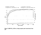
- FIG. 3 shows how the charge capacity for Li 2.65 NiZr 0.18 V 0.60 O x increases slowly then remains constant, for an extended cyclic voltammetry test performed on the sample film.
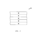
- FIG. 4 includes an illustration of a cross-sectional view of a portion of an electrochromic device.
- electrochromic, lithium ion insertion materials based solely on ternary metal oxides.
- the materials are known as ternary because they consist of a mixture of at least three oxides:
- the first oxide is nickel oxide or a similar anodic electrochromic oxide such as cobalt oxide, iron oxide, iridium oxide or manganese oxide.
- nickel oxide is used over others because of cost, electrochromic efficiency, and favorable optical absorption response.
- a second oxide is believed to significantly modify the structure, optical properties and electrical properties of the anodic, electrochromic oxide, and serves both as a structural host and crystal lattice dopant.
- the second oxides are zirconium oxide, hafnium oxide, tungsten oxide, and niobium oxide.
- the mixed oxide has the formula Li a EC 1 M1 b M2 c O x , where “EC” is the electrochromic metal species, “M1” is the host-oxide metal species, and “M2” is the dopant oxide metal species, and where the subscripts “a”, “1”, “b”, “c”, and “x” denote stoichiometry, or atomic proportions.
- the lithium content (Li a ) is defined for the as-deposited, dark state material, where all the lithium is assumed to be fully oxidized, i.e. in the Li(I) state. This does not, however, preclude the incorporation of reduced state lithium, Li(0), or its chemical analogue, for example a lithium ion, Li+ associated with an electron, when the material is reversibly, electrochemically bleached.
- “a” ranges from about 0.5 to about 3; b+c, which represents the total content of the host oxide species and dopant oxide metal species, ranges from about 0.1 to about 1; c/(b+c), which represents the proportion of dopant metal species to the total of the dopant and host oxide metal species, ranges from about 0.1 to about 0.9; and x, which represents the oxidation stoichiometry, satisfies the charge neutrality.
- “a” ranges from about 1 to about 2.6; b+c, which represents the total content of the host oxide metal species and dopant oxide metal species, ranges from about 0.2 to about 0.45; c/(b+c), which represents the proportion of dopant oxide metal species to the total of the dopant oxide metal species and host oxide metal species, ranges from about 0.55 to about 0.75; and x satisfies the charge neutrality.
- “a” ranges from about 1.4 to about 2.2; b+c, which represents the total content of the host oxide metal species and dopant oxide metal species, ranges from about 0.25 to about 0.35; c/(b+c), which represents the proportion of dopant oxide metal species to the total of the dopant oxide metal species and host oxide metal species, ranges from about 0.6 to about 0.7; and x satisfies the charge neutrality.
- EC is nickel, cobalt, or manganese.
- EC is a mixture of Ni(II) and Ni(III); a mixture of Co(II) and Co(III); a mixture of Ir(IV) and Ir(V); or a mixture of Mn(II), Mn(III), and Mn(IV).
- EC is a mixture of Ni(II) and Ni(III); Co(II) and Co(III); or Ir(IV) and Ir(V).
- EC is a mixture of Ni(II) and Ni(III).
- the second component M1 is zirconium, hafnium, tantalum, niobium, or tungsten.
- the second component M1 (the host-oxide metal species) is Zr(IV); Hf(IV); Ta(V); Nb(V); or W(VI).
- M1 is Zr(IV); Hf(IV); Ta(V); or Nb(V).
- M1 is Zr(IV).
- the third component M2 is selected from vanadium and tantalum.
- the third component M2 (dopant oxide metal species) is V(V); Ta(V); Mo(VI); Nb(V); Mn(IV); La(III); or Ce(IV).
- M2 is V(V); Ta(V); Mo(VI); Nb(V); or Mn(IV).
- M2 is V(V) or Ta(V).
- Representative materials include Li 1.82 NiW 0.45 O x ; Li 1.97 NiZr 0.23 O x ; Li 0.51 NiZr 0.16 La 0.19 O x ; Li 2.22 NiZr 0.14 Mo 0.25 O x ; Li 3.12 NiZr 0.15 Ta 0.15 O x ; and Li 2.65 NiZr 0.18 V 0.60 O x .
- x ranges from about 0.1 to about 50. In some embodiments, x ranges from about 1 to about 6. In other embodiments, x ranges from about 1.6 to about 5.4. Yet other embodiments, including ranges for x, are described in Table I.
- Each of these materials was prepared by using a co-sputter deposition technique, as described herein. All samples were either 80 nm or 200 nm thick. Radio frequency (RF) magnetron sputtering was performed on an Angstrom EvoVac deposition system housed in a glove box under an argon atmosphere following a previously described method.
- RF radio frequency
- the gun powers for the metal alloy targets and ceramic target were about 60 W and about 45 W, respectively.
- the target-substrate distance was 10 cm and remained constant throughout the study, and no additional heating was applied to the substrate.
- the base pressure and total deposition pressure were 10 ⁇ 7 Torr and 2 mTorr, respectively.
- the Ar/O 2 gas mixture was fixed at 1 ⁇ 2 throughout the study.
- the first oxide i.e. the electrochromic oxide
- the electrochromic oxide is believed to segregate to form a nanocrystalline phase, for example, NiO nanocrystals that are dispersed within a substantially amorphous mixture of the remaining oxide material.
- the nanocrystals are mono-disperse, i.e. fall within a narrow size range, while their size can be optimized to promote the effective internal surface or interfacial area of the material.
- the segregation is not complete, and some proportion of the second oxide, or host/dopant oxide, can dope the nanocrystals of the first oxide, in the classical sense of doping by cation substitution. Meanwhile some of the electrochromic material remains alloyed in the amorphous host material.
- the general physical properties of the second oxide are those properties which at least (1) promote doping of the nanocrystal phase by cation substitution, specifically super valent doping to promote ion and electron transport; (2) promote a host oxide molecular structure that minimizes the activation energy for lithium ion diffusion, while maximizing lithium ion mobility; (3) promote the formation of a thermodynamically stable end product, or (4) yield the most desirable optical properties.
- a third oxide further enhances the electrical and optical properties.
- vanadium oxide surprisingly boosts the rate of switching between low and high optical transmission, presumably by boosting both the ionic and electronic conductivity of the electrode material.
- the inventive materials also consist of a significant amount of lithium oxide and/or lithium peroxide.
- anodic electrochromic oxides are believed to form a complex nano-composite material that consists of doped nanocrystals dispersed within an amorphous host material that exhibits surprisingly improved electrochromic performance over the prior art.
- Part of the enhanced performance may result from modifications to the molecular and crystalline structure of composite oxide materials, promoting the transport of lithium ions.
- Part of the enhanced performance may result from aliovalent doping, or super valent doping of the nanocrystalline phase, to promote p-type semiconductor electronic conductivity.
- the ternary compositions disclosed herein, in combination with specific deposition processing conditions yield a material that appears to strike an advantageous balance between elevated ionic and elevated electronic conductivity.
- the vacuum deposition process for growing the electrochromic counter electrode film on a planar substrate is comprised of a simultaneous, mixed, homogenous, uniform, concomitant combined flux (and/or vapor flux) of species that have been sputtered from a sputter target by energetic argon and oxygen ions.
- a magnetron glow discharge may serve as a source, or reservoir, or sputter ions.
- the species include lithium, nickel, zirconium, and a dopant metal such as vanadium, tantalum, or niobium.
- the sputter flux is defined as the amount of atomic species that reach a unit area of substrate per unit time.
- the relative magnitude of the component parts of the sputter flux is determined to a substantial degree by the overall sputter target composition.
- Overall sputter target composition may consist of a collection of pure metal segments, alloy and/or oxide segments, or a finely dispersed composite of metal and/or oxide forms of all of the component species.
- the lithium flux is generated by a separate target, or sputter source, whose voltage, current and sputter flux are separately controlled.
- the sputter flux is combined with the flux of the remaining species to form a homogenous, uniform, resultant flux.
- a major fraction of atoms that have been sputtered from the sputter target surface will arrive at the substrate, while a minor fraction will be lost to the interior walls and sputter shields of the sputter chamber.
- the loss can differ according to atomic mass, where atoms of different mass are scattered by collisions with process gas atoms and molecules to different degrees.
- some major fraction of lithium atoms, nickel atoms, zirconium atoms, and vanadium atoms all arrive at the surface from the lithium oxide sputter target and the Ni—Zr—V alloy target. Proportionally more of the lightest element, lithium, will be lost to walls and shields.
- the sputter target composition or element specific sputter rate can be adjusted to correct for higher loss rates, of, say, lighter atomic species. For example, more power can be applied to the separate lithium oxide sputter target for lithium.
- the composition of a target containing all of the component elements can be empirically enriched with the element(s) most prone to loss, as described above.
- the rate at which all of the remaining atoms arrive, per unit area, per unit time can be regarded as their flux.
- the relative flux of the component atomic species determines composition of the growing film.
- atoms of certain species may stick with less than unit probability, or bounce off the growing film surface.
- the atoms that stick to the surface may be differentially sputtered off of the surface by fast atomic neutral species from the sputter target. This is a well known phenomena for the deposition of indium tin oxide films. These, and additional effects can alter the film composition with respect to the sputter target composition, or collective sputter composition and sputter rates, yet can be corrected by enriching the target or by adjusting sputter power to separate sputter sources for certain elemental components of the film.
- the background partial pressure of oxygen in the sputter gas allows the atomic species that comprise the sputter flux to partially or completely form oxides, of various, mixed oxidation states.
- the overall degree of oxidation can be controlled by controlling the overall magnitude of the sputter flux, and the partial pressure of oxygen.
- Process oxygen is provided as a separate reagent to the sputter (and/or vapor) flux, either partially or in entirety.
- the process oxygen is admixed into the process stream of argon sputter gas.
- the balance of oxygen may be provided by the oxygen content of metal oxides in the sputter source or physical vapor source material.
- the sputter flux and background oxygen yield the growth of a counter electrode material, where the film growth is characterized by the spontaneous, thermodynamically driven segregation of a highly doped, substantially nano-crystalline, nickel oxide component that is dispersed in an amorphous matrix.
- the nano-crystalline component of the material is characterized by larger lattice parameters than those exhibited by pure nickel(II)oxide bunsenite.
- the balance of the material is comprised of a substantially amorphous “host” matrix, in which the nano-crystalline component is dispersed.
- the amorphous matrix may be partially comprised of lithium peroxide.
- the chemical oxidation conditions of the process promote the formation of a substantial proportion of nickel(III) oxide in the deposited film.
- the balance of the nickel comprising the growing films forms nickel(II) oxide.
- the bleached state transparency is at least as high as the prior art LiNiZrO material (as high as about 100% T, in-situ measurement) with depth of coloration as high as about 75%.
- Charge capacities for the new ternary materials range from about 70-85 mC/cm 2 for layers that are approximately 150 nm to 200 nm thick.
- inventive ternary materials offer a brownish tint similar to the current materials, but color to a darker level, for the same amount of electrochemical charge insertion. This allows them to be combined more favorably with dark blue electrochromic tungsten oxide, to yield a more neutral grey dark state for the overall electrochromic coating. In other words, the inventive ternary materials offer higher electrochromic efficiency over an optical wavelength range that is complimentary to electrochromic tungsten oxide.
- the disclosed ternary materials bleach more completely than the prior art materials.
- the depth of coloration may potentially be better than the prior art LiNiZrO x materials but at this point their bleached state transparency is at least comparable to LiNiZrO x .
- little or no perceptible tinting remains when the disclosed materials are in their bleached state.
- the level of yellowness for the overall electrochromic coating in the bleached state can be minimized or eliminated.
- ternary compositions offer the possibility to improve transmission and reflectance modulation in the near infrared region of the solar radiation spectrum, hence the ternary materials are multifunctional electrochromic materials.
- the disclosed materials also exhibit remarkable durability with respect to cycling between their dark and bleached states. No significant level of residual tint builds up in the bleached state with successive cycling. In other words, it is believed that the coating materials are resistant towards turning yellow over the product's (e.g. electrochromic device comprising a layer of this material) service life.
- the interface between the layers will typically form a heterojunction.
- the heterojunction may rectify electronic current, i.e. impose a barrier to electronic current in one direction, forming a diode.
- the heterojunction may also exhibit electronic capacitance. Both effects can limit the performance of the electrochromic film stack, by limiting the rate at which electronic charge can be supplied to (or removed from) the counter electrode through the TCO. Additional effects, both electronic and optical, may arise from the heterojunction. In general, the heterojunction effects will complicate, and very likely degrade, the operation of the electrochromic film stack.
- an excess driving potential or control voltage may be required to surmount the heterojunction barrier, to compensate for capacitance and rectification.
- the excess driving potential will exert greater electrochemical stress on the electrochromic film stack, shortening its service life.
- the excess required potential may exceed the potential window for electrochemical reversibility, leading the irreversible side reactions that degrade product quality.
- Higher driving potentials will also elevate the overall electronic leakage current through defects such as pinholes.
- the addition of the dopant metal oxide to the p-type counter electrode material surprisingly appears to diminish the junction barrier to electronic current between the counter electrode and the n-type TCO, obviating or diminishing the need for both an ohmic contact layer, and/or an excess driving potential.
- the disclosed ternary materials switch faster than the current materials, potentially offering faster switching electrochromic coatings. This also translates into longer product lifetimes for coatings that need not be driven as hard as the current materials. It is believed that this translates into more uniform, aesthetically pleasing visual transitions on going from bleached to dark states.
- FIG. 4 includes an illustration of a cross-sectional view of a portion of an electrochromic device 40 in accordance with an embodiment.
- the electrochromic device 40 includes a first electrode 42 comprising one of a electrochromic layer or a counter electrode layer, a second electrode 44 comprising other of the electrochromic layer or the counter electrode layer, an ion-conductor layer 43 for conducting ions between the first and second electrodes, a first conductive layer 41 , and a second conductive layer 45 , wherein the first and second electrodes 42 and 44 and the ion-conductor layer 43 being sandwiched between the first and second conductive layers 41 and 45 .
- the counter electrode layer comprises a material having a formula Li a EC 1 M1 b M2 c o x , where “EC” is an electrochromic metal species, “M1” is a host-oxide metal species, and “M2” is a dopant oxide metal species, wherein “a” ranges from about 0.5 to about 3, b+c ranges from about 0.1 to about 1, c/(b+c) ranges from about 0.1 to about 0.9, and x is about 0.1 to about 50.
- the NiO nanocrystal size may range about 1.5 nm to about 10 nm.
- the lattice spacing of NiO is affected by the dopant. For example, increased lattice spacing is observed with addition of Zr and V.
- sample films were typically deposited onto 2 mm to 6 mm thick, transparent glass substrates that had been pre-coated with a transparent conductive oxide (“TCO”) layer, typically indium tin oxide (“ITO”) or fluorine doped tin oxide (“FTO”), with a sodium diffusion barrier between the glass substrate and the TCO comprised of silica or a combination of silica and tin oxide layers.
- TCO transparent conductive oxide
- ITO indium tin oxide
- FTO fluorine doped tin oxide
- Other TCO materials could also be used, for example gallium doped zinc oxide or aluminum doped zinc oxide, provided the junction formed between the TCO and counter electrode (“CE”) layers does not interfere with the electrical connection or light transmission.
- substrates other than soda lime glass for example, fused silica, borosilicate glass, or transparent alumina wafers.
- the transparent substrate allows light to be transmitted through the sample as part of the evaluation of electrochromic performance, and electrochromic response to applied potential.
- Representative samples thus prepared were assembled into a three electrode electrochemical cell filled with non-aqueous electrolyte, and connected to an electrochemical potentiostat.
- a precisely defined area of the sample film was immersed in the electrolyte, with the area defined by means of an o-ring seal, platers tape (electroplating tape) or simply the area of substrate film dipped into the liquid electrolyte. This formed the active area of working electrode.
- the active area was connected to the electrochemical potentiostat via the TCO layer, indium solder contact pad, copper tape with conductive silicone adhesive, an alligator clip, and finally a suitably shielded electrical lead.
- Teflon® polytetrafluoroethylene
- a lithium metal reference electrode and a lithium metal auxiliary/counter electrode comprised the remaining two electrodes of the three electrode cell. These were similarly connected to the electrochemical potentiostat via alligator clips and electrical leads.
- the lithium metal reference electrode established an electrochemical reference potential. This reference potential was crucial in that it provided a reproducible, repeatable and unambiguous means of defining the electrochemical potential applied to the sample on an absolute reference scale. It consisted of an unoxidized lithium metal surface in contact with the non-aqueous electrolyte.
- the lithium metal, auxiliary/counter electrode provided an larger active surface of lithium metal, also in contact with the electrolyte.
- the lithium counter electrode served to supply lithium ions to or remove them from the electrolyte to balance the opposite insertion of lithium ions into the sample film or extraction of lithium ions from the sample film.
- the auxiliary/counter electrode completed the electrical circuit through the cell and the potentiostat. Without delving into the detailed function of the operational amplifier circuitry for the potentiostat, the auxiliary/counter electrode supplied the ionic current required to control the potential offset of the working electrode (sample film) with respect to the reference electrode.
- the surface of the reference electrode resided a short distance of about 1 cm or less from the surface of the working electrode, while the surface of the counter electrode resided up to about 4 cm from the working electrode.
- the non-aqueous electrolyte was either purchased (BASF) or prepared from component materials by dissolving a suitable lithium salt such as lithium trifluoromethanesulfonate or lithium perchlorate into a polar, aprotic solvent such as propylene carbonate or ethylene carbonate, or mixture of propylene carbonate and ethylene carbonate.
- a suitable lithium salt such as lithium trifluoromethanesulfonate or lithium perchlorate
- a polar, aprotic solvent such as propylene carbonate or ethylene carbonate, or mixture of propylene carbonate and ethylene carbonate.
- the non-aqueous electrolyte solution was kept free of contamination by water, oxygen, and nitrogen (all reactive with lithium metal) by storing it and handling it under dry argon, either in an inert atmosphere glovebox, or by using inert atmosphere techniques commonly used for synthetic chemistry of air sensitive compounds.
- the concentration of the electrolyte solution was about 0.7 moles per liter, selected to maximize the
- the electrochemical potentiostat was capable of applying a precise and accurate electrochemical potential to the sample film. Moreover, in combination with a digital interface to a personal computer, and suitable control software, the potentiostat was able control the applied potential according to precisely defined, repeatable, and highly versatile protocols of steps, linear ramps, and sinusoidal variation with respect to time, over a wide range of potential, all with respect to the reproducible electrochemical reference potential described above.
- the lithium reference electrode and the lithium counter electrode were combined, both consisting of the same piece of 1 cm ⁇ 2 cm strip of lithium foil dipped into the electrolyte.
- separate lithium metal electrodes were used for the reference and counter electrode, consisting of a 3 mm diameter by 5 mm cylindrical plug of lithium metal extruded through a 5 cm length of rigid wall high density polyethylene [HDPE], or rigid nylon, 6 mm tubing.
- HDPE was preferred because of low its propensity for water uptake and permeation, similar to Teflon®.
- Light from a diode laser or a light emitting diode was optionally shone through the entire assembly of the sample film and the three electrode cell.
- the light path optionally traversed an o-ring sealed window (to contain the liquid electrolyte) formed by the sample substrate itself, and then a second, uncoated glass window on the opposite side of the cell.
- the sample substrate was dipped into electrolyte between two parallel windows comprising opposite walls of the cell.
- Light passing through the cell was directed onto a suitable light sensor, typically an integrated circuit equipped with a photodiode and transimpedance amplifier (an operational amplifier that converts current to voltage).
- Light intensity was then recorded by means of sampling the amplified output that had been converted from photo-current to voltage and then connected to an analogue to digital signal acquisition circuit (ADC or DAQ) where light intensity could be recorded as a function of time, in synchrony with the current and voltage signals for the electrochemical potentiostat, and stored in a computer text file written to a hard drive.
- the light intensity scale was defined by setting the voltage for a reference blank cell (all cell components in the optical path, except the sample film) to 100% transmission, and the voltage with the light source (diode laser or LED) off, to 0% transmission. Care was taken not to saturate the photodiode with excessive light intensity, so that the signal linearity (proportionality between light intensity and photo signal voltage) could be assured.
- a simplified optical train consisted of a red diode laser (670 nm) shining through the sample cell assembly directly onto a light sensor.
- output from a white LED was collimated (optically refracted from a divergent cone of rays into a cylinder of parallel rays) by a commercially available achromatic doublet lens (Thorlabs), or an anastigmatic lens assembly (Viewlux Anastigmat surplus slide projector lens).
- Thixorlabs achromatic doublet lens
- an anastigmatic lens assembly Viewlux Anastigmat surplus slide projector lens
- the combination of white LED and photo detector was optionally selected to approximate the photopic sensitivity (bright light color response) of a standard human observer.
- the electrochemical range of interest for nickel oxide based electrochromic films typically spans about +1.5 Volts to about +5.0 Volts versus the potential of a lithium reference electrode in about 0.7 to about 1.0 moles per liter lithium electrolyte. At potentials near about +1.5 Volts, irreversible, electrochemical reduction reactions tend to occur. In this context, metal oxide species undergoing electrochemical reduction form lower oxides (fewer oxygen atoms per metal atom) or fully reduced metallic species. Near about +5.0 Volts, irreversible oxidation reactions tend to occur, notably the irreversible oxidation of nickel species to the about +3 and higher oxidation states, with concomitant degradation of the optical properties, for example, irreversible loss of bleached state transmission.
- potentiostats can be programmed to automatically perform a series of electrochemical tests, to repeatedly switch sample films between lithium extracted, oxidized, dark, Ni about +3 electrochromic state and the lithium ion inserted, reduced, bleached, Ni about +2 electrochromic state.
- the electrochemical potential can be stepped, scanned and modulated between potential limits, precisely, accurately and repeatedly, while recording current, voltage, and the percent of transmitted light intensity.
- Two test protocols used to characterize samples of ternary metal oxide counter electrode films are cyclic voltammetry and chronoamperometry.
- a simplified form of chronoamperometry consists of abruptly stepping the potential applied to the sample film from an oxidizing, dark state, ion extracting potential to a reducing, bleached state, ion inserting potential, and then repeating this step cycle for hundreds of repetitions. For every step, the response of both the current and light intensity are recorded according to a sampling interval frequency several times faster than the cycle frequency.
- the charge capacity of the sample film i.e. the quantity of ions, expressed as Coulombs per unit area of sample film, can be determined by numerically integrating the current with respect to time.
- This protocol can also gauge the rate at which the film darkens or bleaches, and the ultimate transmission levels of the dark and bleached states. Over several tens or hundreds of step cycles, this protocol indicates the stability of the sample or its propensity to fade, or diminish in capacity with cycling.
- Cyclic Voltammetry is analogous to chronoamperometry except that the potential applied to the sample not stepped abruptly between potential limits, but scanned at a constant rate, say about 2 mV/s to about 200 mV/s, between potential limits.
- the current signal from this technique can also be numerically integrated to obtain an charge capacity, and its respective stability, but the charge capacity for cyclic voltammetry typically differs from that for chronoamperometry.
- cyclic voltammetry does not yield a rate of coloration or bleaching in response to a potential step, but reveals the potential where the oxidation and reduction processes begin.
- the shape of the current response can also indicate whether cycling between dark and bleached states is electrochemically reversible.
- the time interval required to bleach the sample through 90% of its full transmission range was about 11 seconds, on average. i.e. the bleaching time, tb, was approximately 11 seconds, on average.
- the coloration time and bleaching time provide a convenient indication of how fast the electrode sample switches between dark and bleached states and vise versa.
- About 11 seconds represents an improvement of approximately 5 times over previously evaluated compositions, ones that omitted the vanadium dopant oxide.
- the addition of the vanadium dopant oxide surprisingly and beneficially accelerated the coloration and bleaching rates of the ternary composition. It may have done so by boosting the lithium ion conductivity and diffusivity through the bulk material, or by minimizing contact resistance or heterojunction potential at the interface between the ternary composition counter electrode layer and the TCO layer (in this case, FTO).
- the coloration time, tc increased to about 25 s
- the bleaching time, tb increased to about 12 s, on average, again, where tc is the time required to “color” or decrease the optical transmission through 90% of its full range, and where Tb is the time required to “bleach” or increase the optical transmission through 90% of its full range.
- the reversible lithium ion capacity for the Li 2.65 NiZr 0.18 V 0.60 O x composition exhibited minimal fade of less than about 20% reduction of measured charge capacity over about 500 cycles. This reveals that the disclosed ternary compositions retain the charge capacity at least as well as the prior art binary materials.
- the ternary compositions exhibited excellent electrochromic efficiency in the blue region of the visible spectrum (visible wavelength range of 420 nm to 480 nm), where the electrochromic efficiency represents the change in optical density for a corresponding quantity of charge inserted or extracted from the sample, expressed in terms of inverse units of charge per unit area. Measured values were about 30-40 cm 2 /C in the blue region of the visible spectrum, decreasing to less than about 20 at red wavelengths greater than 600 nm.
- a sample film were stepped from a bleached state holding potential of about 1.7 Volts versus of the lithium reference potential to about 4.2 Volts, then the total charge of lithium ions extracted from the sample (determined by numerically integrating the current) was typically about 40 mC/cm 2 .
- a sample electrode of Li 2.65 NiZr 0.48 V 0.60 O (3.9 to 5.4) was deposited as follows:
- a custom metal sputter target composed of 70 atm % nickel, 15 atm % zirconium and 15 atm % vanadium was purchased from ACI alloys (San Jose Calif.).
- the metal sputter target was loaded into a 3 inch diameter, commercially available sputter source, within a vacuum system from the same vendor (Angstrom Engineering, Kitchener, ON), alongside an identical twin sputter sputter source loaded with a lithium oxide target bonded to a molybdenum backing plate, purchased from Plasmaterials, Inc. (Livermore, Calif.).
- the entire sputter system was housed within an argon atmosphere glove box (M.
- the argon atmosphere glove box allowed the sample substrates to be loaded into the sputter system, and the substrates subsequently coated with sample films to be removed, all under an inert atmosphere of argon gas.
- the soda lime substrate glass for the sample films had been pre-coated with fluorine doped tin oxide, upon a layer of silicon dioxide, upon a layer of tin oxide.
- These pre-coated substrates were available as Pilkington Tec Glass, specifically, Pilkington Tec 15, supplied by Hartford Glass (Hartford City, Ind.).
- the sheet resistance, (“Rs”), of the fluorine doped tin layer was about 15 Ohms per square. Its conductivity, ⁇ , was approximately 2 ⁇ 10 3 S/cm, or approximately 5 times less conductive than high quality indium tin oxide.
- the substrates Prior to sample deposition, the substrates were cleaned successively with soapy water, deionized water, acetone, isopropyl alcohol, and dried under a flowing stream of nitrogen gas.
- the pre-coated substrate glass was attached using Kapton (Dupont, Wilmington, Del.) polyimide tape, with silicone adhesive, to a 15 cm ⁇ 15 cm copper plate.
- the copper plate was then mounted onto a motorized, rotary shaft extending down from the ceiling of the vacuum chamber.
- the substrate faced directly down at the two sputter sources described above, at a distance of 10 cm from the sputter target.
- the copper plate and substrate were rotated to average out the composition of sputtered flux of atomic species reaching the substrate surface.
- the vacuum chamber that housed the sputter sources was pumped down first to rough vacuum by mechanical vacuum pumps, and then down to a high vacuum base pressure of ⁇ 1 ⁇ 10 ⁇ 7 Torr by means of a helium cryo-pump (Cryo-torr 8F, CTI Cryogenics). Pumping the chamber down to this based pressure ensured that the process was not contaminated by air or water leaks or from gaseous species outgassing from components within the vacuum chamber.
- sputter deposition For sputter deposition, a mixture of argon and oxygen sputter gas was admitted into the vacuum chamber at a volumetric flow rate ratio of 1 to 2 for Argon to Oxygen. The total flow rate was increased while the pumping port leading to the cryo-pump was throttled, to achieve a constant sputter pressure of about 2 milliTorr. Radio frequency (rf) power was supplied to the sputter targets at a frequency of about 13.56 MHz.
- rf Radio frequency
- rf power was supplied to the sputter source with the nickel-zirconium-vanadium sputter target, to sustain a target power density (applied power divided by total target area) of about 1.1 Watts per cm 2
- a target power density applied power divided by total target area
- about 45 Watts of rf power was supplied to the sputter source with the lithium oxide ceramic sputter target, to sustain a target power of about 0.83 Watts per cm 2 .
- These sputter conditions yielded a sample film growth rate (or deposition rate) of about 0.04 ⁇ ngstroms per second.
- the resulting sample film was removed and sectioned into 1 cm ⁇ 2 cm slides for further characterization by electrochemical cyclic voltammetry and chronoamperometry, and for spectrophotometric characterization.
- ICP-MS inductively coupled plasma mass spectrometry
- sample films contained nickel oxide nanocrystals with a characteristic size of 3.5 nm (35 ⁇ ngstoms in diameter).
- Elemental analysis by ICP-MS revealed that the relative atomic metals composition was about 2.65:1.00:0.18:0.60 for lithium:nickel:zirconium:vanadium.
- the sample films When subjected to cyclic voltammetry, scan-cycling at about 20 milliVolts per second between about 1.7 Volts to about 4.2 Volts versus a lithium reference electrode, the sample films showed excellent reversibility: films (80 and 200 nm thick) exhibited less than 20% fade in charge capacity after 500 scan-cycles from 1.7 to 4.2 and back to 1.7 Volts. Chronoamperometry tests subjected the sample films to abrupt, repeating steps in electrochemical potential from 1.7 Volts to 4.2 Volts (coloration step) and 4.2 Volts to 1.7 Volts (bleaching step) with a 2 minute time interval between steps.
- Li 1.97 NiZr 0.23 O x electrode samples was exactly analogous to that for Li 2.65 NiZr 0.18 V 0.60 Ox except that the metal sputter target composition was 80 atm % nickel and 20 atm % zirconium.
- sample films contained nickel oxide nanocrystals with a characteristic size of 3.4 nm (34 ⁇ ngstoms in diameter).
- the sample films showed excellent reversibility through cyclic voltammetry: films (about 80 and about 200 nm thick) exhibited less than about 20% fade in charge capacity after 500 scan-cycles from 1.7 to 4.2 and back to 1.7 Volts.
Landscapes
- Chemical & Material Sciences (AREA)
- Physics & Mathematics (AREA)
- Chemical Kinetics & Catalysis (AREA)
- Nonlinear Science (AREA)
- Engineering & Computer Science (AREA)
- Electrochemistry (AREA)
- General Chemical & Material Sciences (AREA)
- Inorganic Chemistry (AREA)
- Materials Engineering (AREA)
- Mechanical Engineering (AREA)
- Metallurgy (AREA)
- Organic Chemistry (AREA)
- Optics & Photonics (AREA)
- General Physics & Mathematics (AREA)
- Manufacturing & Machinery (AREA)
- Crystallography & Structural Chemistry (AREA)
- Electrochromic Elements, Electrophoresis, Or Variable Reflection Or Absorption Elements (AREA)
- Inorganic Compounds Of Heavy Metals (AREA)
Priority Applications (1)
| Application Number | Priority Date | Filing Date | Title |
|---|---|---|---|
| US13/961,184 US8995041B2 (en) | 2012-08-09 | 2013-08-07 | Ternary nickel oxide materials for electrochromic devices |
Applications Claiming Priority (3)
| Application Number | Priority Date | Filing Date | Title |
|---|---|---|---|
| US201261681353P | 2012-08-09 | 2012-08-09 | |
| US201361776886P | 2013-03-12 | 2013-03-12 | |
| US13/961,184 US8995041B2 (en) | 2012-08-09 | 2013-08-07 | Ternary nickel oxide materials for electrochromic devices |
Publications (2)
| Publication Number | Publication Date |
|---|---|
| US20140043666A1 US20140043666A1 (en) | 2014-02-13 |
| US8995041B2 true US8995041B2 (en) | 2015-03-31 |
Family
ID=49029211
Family Applications (1)
| Application Number | Title | Priority Date | Filing Date |
|---|---|---|---|
| US13/961,184 Active US8995041B2 (en) | 2012-08-09 | 2013-08-07 | Ternary nickel oxide materials for electrochromic devices |
Country Status (5)
| Country | Link |
|---|---|
| US (1) | US8995041B2 (fr) |
| EP (2) | EP3543781B1 (fr) |
| JP (1) | JP6279578B2 (fr) |
| CN (1) | CN105008992B (fr) |
| WO (1) | WO2014025876A2 (fr) |
Cited By (11)
| Publication number | Priority date | Publication date | Assignee | Title |
|---|---|---|---|---|
| US9753348B2 (en) | 2013-01-21 | 2017-09-05 | Kinestral Technologies, Inc. | Electrochromic lithium nickel group 5 mixed metal oxides |
| US10095079B2 (en) | 2013-01-21 | 2018-10-09 | Kinestral Technologies, Inc. | Electrochromic lithium nickel group 4 mixed metal oxides |
| JP2022141789A (ja) * | 2015-07-14 | 2022-09-29 | ビュー, インコーポレイテッド | エレクトロクロミックデバイス用の対電極 |
| US11891327B2 (en) | 2014-05-02 | 2024-02-06 | View, Inc. | Fabrication of low defectivity electrochromic devices |
| US11898233B2 (en) | 2009-03-31 | 2024-02-13 | View, Inc. | Electrochromic devices |
| US11947232B2 (en) | 2009-03-31 | 2024-04-02 | View, Inc. | Fabrication of low defectivity electrochromic devices |
| US11960188B2 (en) | 2014-11-26 | 2024-04-16 | View, Inc. | Counter electrode for electrochromic devices |
| US11966140B2 (en) | 2009-03-31 | 2024-04-23 | View, Inc. | Counter electrode for electrochromic devices |
| US12043890B2 (en) | 2009-03-31 | 2024-07-23 | View, Inc. | Electrochromic devices |
| US12209048B2 (en) | 2009-03-31 | 2025-01-28 | View, Inc. | Counter electrode for electrochromic devices |
| US12353109B2 (en) | 2009-12-22 | 2025-07-08 | View Operating Corporation | Electrochromic cathode materials |
Families Citing this family (17)
| Publication number | Priority date | Publication date | Assignee | Title |
|---|---|---|---|---|
| US10261381B2 (en) | 2009-03-31 | 2019-04-16 | View, Inc. | Fabrication of low defectivity electrochromic devices |
| US11187954B2 (en) | 2009-03-31 | 2021-11-30 | View, Inc. | Electrochromic cathode materials |
| US10852613B2 (en) | 2009-03-31 | 2020-12-01 | View, Inc. | Counter electrode material for electrochromic devices |
| US9261751B2 (en) | 2010-04-30 | 2016-02-16 | View, Inc. | Electrochromic devices |
| US9759975B2 (en) | 2010-04-30 | 2017-09-12 | View, Inc. | Electrochromic devices |
| CN107300819B (zh) | 2011-07-21 | 2021-03-12 | Sage电致变色显示有限公司 | 同时掺杂有锂和金属掺杂物的电致变色的镍氧化物 |
| US10345671B2 (en) | 2014-09-05 | 2019-07-09 | View, Inc. | Counter electrode for electrochromic devices |
| CN106086797B (zh) * | 2016-07-12 | 2018-12-11 | 京东方科技集团股份有限公司 | 氧化铟锡薄膜及其制备方法、含其的阵列基板、显示装置 |
| CN108254989B (zh) * | 2016-12-29 | 2020-09-29 | 宁波祢若电子科技有限公司 | 全固态电致变色窗和固态电致变色镜及其制备方法 |
| CA3070511A1 (fr) | 2017-07-20 | 2019-01-24 | Click Materials Corp. | Photodeposition d'oxydes metalliques pour dispositifs electrochromes |
| US11866647B2 (en) | 2018-07-18 | 2024-01-09 | Comberry, Llc | Electrochromic material and method of manufacturing thereof |
| FR3088850B1 (fr) * | 2018-11-28 | 2020-12-11 | Saint Gobain | Procede de fabrication d’un vitrage electrochrome |
| CN109809499B (zh) * | 2019-01-09 | 2021-03-19 | 蜂巢能源科技有限公司 | 富锂正极材料前驱体、富锂正极材料及其制备方法 |
| US11703737B2 (en) | 2020-02-12 | 2023-07-18 | Sage Electrochromics, Inc. | Forming electrochromic stacks using at most one metallic lithium deposition station |
| TWI739419B (zh) * | 2020-05-08 | 2021-09-11 | 崑山科技大學 | 電致變色材料的製作方法 |
| US20230176350A1 (en) * | 2021-12-03 | 2023-06-08 | Samsung Electronics Co., Ltd. | Multiple fields-of-view lens |
| EP4692917A1 (fr) * | 2024-08-09 | 2026-02-11 | Saint-Gobain Glass France | Oxyde de nickel-tungstène-zirconium pour dispositifs électrochromiques |
Citations (9)
| Publication number | Priority date | Publication date | Assignee | Title |
|---|---|---|---|---|
| US5699192A (en) | 1992-04-10 | 1997-12-16 | Sun Active Glass Electrochromics, Inc. | Electrochromic structures and methods |
| US6094292A (en) | 1997-10-15 | 2000-07-25 | Trustees Of Tufts College | Electrochromic window with high reflectivity modulation |
| US6277532B1 (en) | 1998-10-14 | 2001-08-21 | Nikon Corporation | Charged-particle-beam microlithographic methods for correction of reticle distortions |
| US20040150867A1 (en) | 2001-08-07 | 2004-08-05 | Se-Hee Lee | Electrochromic counter electrode |
| US20040155263A1 (en) | 1996-03-27 | 2004-08-12 | Saint-Gobain Vitrage | Electrochemical device |
| US20060028730A1 (en) | 1994-05-05 | 2006-02-09 | Donnelly Corporation | Electrochromic mirrors and devices |
| US20090057137A1 (en) | 2007-08-31 | 2009-03-05 | Midwest Research Institute | Synthesizing thin films of lithiated transition metal oxide for use in electrochemical and battery devices |
| WO2009029111A1 (fr) | 2007-08-31 | 2009-03-05 | Midwest Research Institute | Batteries à base de lithium à film fin et dispositifs électrochromiques fabriqués avec des matériaux d'électrode nanocomposites |
| US20140016173A1 (en) * | 2011-07-21 | 2014-01-16 | National Renewable Energy Laboratory | Electrochromic nickel oxide simultaneously doped with lithium and a metal dopant |
Family Cites Families (6)
| Publication number | Priority date | Publication date | Assignee | Title |
|---|---|---|---|---|
| US7133181B2 (en) * | 2004-07-23 | 2006-11-07 | Sage Electrochromics, Inc. | Control system for electrochromic devices |
| US7372610B2 (en) * | 2005-02-23 | 2008-05-13 | Sage Electrochromics, Inc. | Electrochromic devices and methods |
| US7593154B2 (en) * | 2005-10-11 | 2009-09-22 | Sage Electrochromics, Inc. | Electrochromic devices having improved ion conducting layers |
| FR2904704B1 (fr) * | 2006-08-04 | 2008-12-05 | Saint Gobain | Dispositif electrochimique, et/ou elelctrocommandable du type vitrage et a proprietes optiques et/ou energetiques variables |
| EP2089764B1 (fr) * | 2006-11-09 | 2016-01-06 | Sage Electrochromics, Inc. | Procédé permettant de fabriquer un dispositif de commutation des ions sans étape de lithiation distincte |
| WO2009031422A1 (fr) * | 2007-09-05 | 2009-03-12 | Kuraray Co., Ltd. | Procédé de fabrication d'un dispositif d'affichage électrochromique |
-
2013
- 2013-08-07 EP EP19174419.2A patent/EP3543781B1/fr active Active
- 2013-08-07 EP EP13752751.1A patent/EP2883107B1/fr active Active
- 2013-08-07 WO PCT/US2013/053934 patent/WO2014025876A2/fr not_active Ceased
- 2013-08-07 CN CN201380049640.5A patent/CN105008992B/zh active Active
- 2013-08-07 US US13/961,184 patent/US8995041B2/en active Active
- 2013-08-07 JP JP2015526668A patent/JP6279578B2/ja not_active Expired - Fee Related
Patent Citations (11)
| Publication number | Priority date | Publication date | Assignee | Title |
|---|---|---|---|---|
| US5699192A (en) | 1992-04-10 | 1997-12-16 | Sun Active Glass Electrochromics, Inc. | Electrochromic structures and methods |
| US20060028730A1 (en) | 1994-05-05 | 2006-02-09 | Donnelly Corporation | Electrochromic mirrors and devices |
| US20040155263A1 (en) | 1996-03-27 | 2004-08-12 | Saint-Gobain Vitrage | Electrochemical device |
| US6094292A (en) | 1997-10-15 | 2000-07-25 | Trustees Of Tufts College | Electrochromic window with high reflectivity modulation |
| US6277532B1 (en) | 1998-10-14 | 2001-08-21 | Nikon Corporation | Charged-particle-beam microlithographic methods for correction of reticle distortions |
| US20040150867A1 (en) | 2001-08-07 | 2004-08-05 | Se-Hee Lee | Electrochromic counter electrode |
| US6859297B2 (en) | 2001-08-07 | 2005-02-22 | Midwest Research Institute | Electrochromic counter electrode |
| US20090057137A1 (en) | 2007-08-31 | 2009-03-05 | Midwest Research Institute | Synthesizing thin films of lithiated transition metal oxide for use in electrochemical and battery devices |
| WO2009029111A1 (fr) | 2007-08-31 | 2009-03-05 | Midwest Research Institute | Batteries à base de lithium à film fin et dispositifs électrochromiques fabriqués avec des matériaux d'électrode nanocomposites |
| US20110151283A1 (en) | 2007-08-31 | 2011-06-23 | Alliance For Sustainable Energy, Llc. | Thin film lithium-based batteries and electrochromic devices fabricated with nanocomposite electrode materials |
| US20140016173A1 (en) * | 2011-07-21 | 2014-01-16 | National Renewable Energy Laboratory | Electrochromic nickel oxide simultaneously doped with lithium and a metal dopant |
Non-Patent Citations (30)
| Title |
|---|
| C. Pouillerie et al.: "Effect of magnesium substitution on the cycling behavior of lithium nickel cobalt oxide", Journal of Power Sources, vol. 96, 2001, pp. 293-302. |
| Dane Gillaspie et al: "Nanocomposite Counter Electrode Materials for Electrochromic Windows", Journal of the Electrochemical Society, vol. 157, No. 3, Jan. 20, 2010, pp. H328-H331, XP055095795. |
| Dane T. Gillaspie et al: ‘Metal-oxide films for electrochromic applications: present technology and future directions’, Journal of Materials Chemistry, vol. 20, No. 43, Jan. 10, 2010, pp. 9585-9592, XP055095800. |
| Dane T. Gillaspie et al: 'Metal-oxide films for electrochromic applications: present technology and future directions', Journal of Materials Chemistry, vol. 20, No. 43, Jan. 10, 2010, pp. 9585-9592, XP055095800. |
| European Search Report for Application No. EP 06003692 dated May 9, 2002. |
| International Search Report and Written Opinion for Application No. PCT/US2013/053934 dated Apr. 23, 2014. |
| International Search Report for Application No. PCT/US2012/047569 dated Sep. 19, 2012. |
| J. Kim, K. Amine: "A comparative study on the substitution of divalent, trivalent and tetravalent metal ions in LiNi1-xMx02 (M=Cu2+, A13+ and Ti4+)", Journal of Power Sources, vol. 104, 2002, pp. 33-39. |
| J.B. Wu et .al.: "Analysis of AC electrical properties of (Li and Ti)-doped NiO", Materials Science and Engineering B, vol. 99, 2003, pp. 294-297. |
| Kaufman, H.R. et al., Sputtering, J. Vac. Sci. Techn. 21, 725 (1982). |
| Kenji Tateishi et al: ‘LiMn204: a spinel-related low-temperature modification’, Acta Crystallographica Section E Structure Reports Online, vol. 60, No. 2, Jan. 17, 2004, pp. i18-i21, XP055096067. |
| Kenji Tateishi et al: 'LiMn204: a spinel-related low-temperature modification', Acta Crystallographica Section E Structure Reports Online, vol. 60, No. 2, Jan. 17, 2004, pp. i18-i21, XP055096067. |
| Lee et al., "A new lithium based counter electrochromic material for fast optical reponse", Proceedings of the third symposium on Electrochromic Materials, vol. 96-24, 1997, pp. 191-205. |
| Lee S-H et al: "Characterization of Ni-W oxide thin film electrodes" Solid State Ionics, North Holland Pub. Company. Amsterdam, NL, vol. 109, No. 3-4, Jun. 2, 1998, pp. 303-310. |
| Lee S-H et al: "Characterization of Ni—W oxide thin film electrodes" Solid State Ionics, North Holland Pub. Company. Amsterdam, NL, vol. 109, No. 3-4, Jun. 2, 1998, pp. 303-310. |
| Lee S-H et al: "Raman spectroscopic studies of Ni-W oxide thin films" Solid State Ionics, North Holland Pub. Company. Amsterdam, NL, vol. 140, No. 1-2, Mar. 1, 2001, pp. 135-139. |
| Lee S-H et al: "Raman spectroscopic studies of Ni—W oxide thin films" Solid State Ionics, North Holland Pub. Company. Amsterdam, NL, vol. 140, No. 1-2, Mar. 1, 2001, pp. 135-139. |
| Lee, S.-H. et al., "Electrochromic behavior of Ni-W oxide electrodes," Solar energy Materials and Solar Cells 39 (1995) 155-166. |
| Lee, S.-H. et al., "Electrochromic behavior of Ni—W oxide electrodes," Solar energy Materials and Solar Cells 39 (1995) 155-166. |
| Lee, Se-Hee et al., "Electrochromic mechanism in a-WO3-y thin films," Applied Physics Letters, American Institute of Physics (Jan. 11, 1999), pp. 242-244. |
| Lim s et al: "PVP-Assisted Zr02 coating on LiMn204 spinel cathode nanoparticles prepared by Mn02 nanowire templates", Electrochemistry Communications, Elsevier, Amsterdam, NL, vol. 10, No. 10, Oct. 1, 2008, pp. 1478-1481, XP025467154. |
| P. M. S. Monk, R. J. Mortimer, D. R. Rosseinsky: "Electrochromism: Fundamentals and Applications", 1995, VCH, Federal Republic of Germany, XP002718689, pp. 78-91. |
| Passerini S et al: "The Intercalation of Lithium in Nickel Oxide and Its Electrochromic Properties" Journal of the Electrochemical Society, Electrochemical Society. Manchester, New Hampshire, US, vol. 137, No. 10, Oct. 1, 1990, pp. 3297-3300. |
| Paul M. S. Monk et al: ‘Electrochromic tungsten oxide: doping with two or three other metal oxides’, Journal of Materials Chemistry, vol. 4, No. 7, 1994, pp. 1071-1074, XP055095387. |
| Paul M. S. Monk et al: 'Electrochromic tungsten oxide: doping with two or three other metal oxides', Journal of Materials Chemistry, vol. 4, No. 7, 1994, pp. 1071-1074, XP055095387. |
| Scrosati, "1st International Meeting on Electrochromism (IME-1), Murano-Venice, Oct. 19-21, 1994", Solar Energy Materials and Solar Cells, 1995. |
| Svegl F et al: "Electrochromic properties of lithiated Co-oxide (LixCo02) and Ni-oxide (LixNi02) thin films prepared by the sol-gel route", Solar Energy. Pergamon Press. Oxford, GB, vol. 68, No. 6, Jan. 1, 2000, pp. 523-540. |
| Svegl F et al: "Electrochromic properties of lithiated Co-oxide (LixCo02) and Ni—oxide (LixNi02) thin films prepared by the sol-gel route", Solar Energy. Pergamon Press. Oxford, GB, vol. 68, No. 6, Jan. 1, 2000, pp. 523-540. |
| Yan Dong et .al.: "Microstructure and dielectric properties of LiTiNiO thin films", Key Engineering Materials, vol. 336-338, 2007, pp. 2635-2638. |
| Z. Lu, J.R. Dahn: "Understanding the anomalous capacity of Li/Li [NixLi (1/3-2x/3)Mn(2/3-x/3]02 cells using in situ X-ray diffraction and electrochemical studies", Journal of the Electrochemical Society, vol. 149, 2002, pp. A815-A822. |
Cited By (16)
| Publication number | Priority date | Publication date | Assignee | Title |
|---|---|---|---|---|
| US11966140B2 (en) | 2009-03-31 | 2024-04-23 | View, Inc. | Counter electrode for electrochromic devices |
| US12242163B2 (en) | 2009-03-31 | 2025-03-04 | View, Inc. | Fabrication of low defectivity electrochromic devices |
| US11947232B2 (en) | 2009-03-31 | 2024-04-02 | View, Inc. | Fabrication of low defectivity electrochromic devices |
| US12209048B2 (en) | 2009-03-31 | 2025-01-28 | View, Inc. | Counter electrode for electrochromic devices |
| US12443085B2 (en) | 2009-03-31 | 2025-10-14 | View Operating Corporation | Counter electrode for electrochromic devices |
| US12043890B2 (en) | 2009-03-31 | 2024-07-23 | View, Inc. | Electrochromic devices |
| US11898233B2 (en) | 2009-03-31 | 2024-02-13 | View, Inc. | Electrochromic devices |
| US12366784B2 (en) | 2009-12-22 | 2025-07-22 | View Operating Corporation | Electrochromic cathode materials |
| US12353109B2 (en) | 2009-12-22 | 2025-07-08 | View Operating Corporation | Electrochromic cathode materials |
| US9753348B2 (en) | 2013-01-21 | 2017-09-05 | Kinestral Technologies, Inc. | Electrochromic lithium nickel group 5 mixed metal oxides |
| US10095079B2 (en) | 2013-01-21 | 2018-10-09 | Kinestral Technologies, Inc. | Electrochromic lithium nickel group 4 mixed metal oxides |
| US10845666B2 (en) | 2013-01-21 | 2020-11-24 | Kinestral Technologies, Inc. | Electrochromic lithium nickel group 5 mixed metal oxides |
| US10739657B2 (en) | 2013-01-21 | 2020-08-11 | Kinestral Technologies, Inc. | Electrochromic lithium nickel group 4 mixed metal oxides |
| US11891327B2 (en) | 2014-05-02 | 2024-02-06 | View, Inc. | Fabrication of low defectivity electrochromic devices |
| US11960188B2 (en) | 2014-11-26 | 2024-04-16 | View, Inc. | Counter electrode for electrochromic devices |
| JP2022141789A (ja) * | 2015-07-14 | 2022-09-29 | ビュー, インコーポレイテッド | エレクトロクロミックデバイス用の対電極 |
Also Published As
| Publication number | Publication date |
|---|---|
| EP2883107B1 (fr) | 2019-05-15 |
| JP6279578B2 (ja) | 2018-02-14 |
| US20140043666A1 (en) | 2014-02-13 |
| WO2014025876A3 (fr) | 2014-06-12 |
| WO2014025876A2 (fr) | 2014-02-13 |
| EP3543781A1 (fr) | 2019-09-25 |
| JP2016526173A (ja) | 2016-09-01 |
| CN105008992A (zh) | 2015-10-28 |
| CN105008992B (zh) | 2018-01-09 |
| EP2883107A2 (fr) | 2015-06-17 |
| EP3543781B1 (fr) | 2022-10-12 |
Similar Documents
| Publication | Publication Date | Title |
|---|---|---|
| US8995041B2 (en) | Ternary nickel oxide materials for electrochromic devices | |
| US6859297B2 (en) | Electrochromic counter electrode | |
| Lee et al. | Electrochromic coloration efficiency of a-WO 3− y thin films as a function of oxygen deficiency | |
| Monk et al. | Electrochromism: fundamentals and applications | |
| Zhang et al. | The influence of microstructure on the electrochromic properties of LixWO3 thin films: Part I. Ion diffusion and electrochromic properties | |
| EP0568524B1 (fr) | Element composite comportant une couche en chalcogenure ou oxychalcogenure de titane, utilisable en particulier comme electrode positive dans une cellule electrochimique en couches minces | |
| Yoshimura et al. | Nickel oxide electrochromic thin films prepared by reactive DC magnetron sputtering | |
| Colton et al. | Electrochromism in some thin‐film transition‐metal oxides characterized by x‐ray electron spectroscopy | |
| RU2761772C1 (ru) | Электрохромный материал и способ его изготовления | |
| Mak et al. | Effect of Al doping on the electrochromic properties of WO3 thin films | |
| Lindgren et al. | Photoelectrochemical characterisation of indium nitride and tin nitride in aqueous solution | |
| Bressers et al. | The electrochromic behavior of indium tin oxide in propylene carbonate solutions | |
| Svensson et al. | Electrochromism of nickel-based sputtered coatings | |
| US5164855A (en) | Counter electrode for electrochromic systems | |
| US20070076286A1 (en) | Electrochromic device comprising protective inorganic solid electrolyte film and manufacturing method thereof | |
| Kullman et al. | Decreased electrochromism in Li-intercalated Ti oxide films containing La, Ce, and Pr | |
| JP3211036B2 (ja) | リチウムイオンでインターカレーションされた酸化ニッケル電極 | |
| Bohnke et al. | Electrochromic properties of polycrystalline thin films of tungsten trioxide prepared by chemical vapour deposition | |
| Azens et al. | Electrochromism of fluorinated and electron‐bombarded tungsten oxide films | |
| WO2003014254A1 (fr) | Contre-electrode electrochrome | |
| Hanzu et al. | In situ study of electrochromic properties of self-assembled TiO2 nanotubes | |
| Erlandsson et al. | Electrochromic properties of manganese oxide (MnOx) thin films made by electron beam deposition | |
| Niklasson et al. | Durability of electrochromic films: aging kinetics and rejuvenation | |
| Zanoni et al. | Surface evolution of Ni–V transparent oxide films upon Li insertion reactions | |
| Baucke | Electrochromic mirrors with variable reflectance |
Legal Events
| Date | Code | Title | Description |
|---|---|---|---|
| AS | Assignment |
Owner name: ALLIANCE FOR SUSTAINABLE ENERGY, LLC, COLORADO Free format text: ASSIGNMENT OF ASSIGNORS INTEREST;ASSIGNORS:ENGTRAKUL, CHAIWAT;LIN, FENG;SIGNING DATES FROM 20131108 TO 20131118;REEL/FRAME:031640/0026 |
|
| AS | Assignment |
Owner name: SAGE ELECTROCHROMICS,INC., MINNESOTA Free format text: ASSIGNMENT OF ASSIGNORS INTEREST;ASSIGNOR:WEIR, DOUGLAS GLENN JOHN;REEL/FRAME:031856/0530 Effective date: 20131014 |
|
| STCF | Information on status: patent grant |
Free format text: PATENTED CASE |
|
| AS | Assignment |
Owner name: ENERGY, UNITED STATES DEPARTMENT OF, DISTRICT OF C Free format text: CONFIRMATORY LICENSE;ASSIGNOR:ALLIANCE FOR SUSTAINABLE ENERGY, LLC;REEL/FRAME:036816/0950 Effective date: 20150807 |
|
| FEPP | Fee payment procedure |
Free format text: PAYOR NUMBER ASSIGNED (ORIGINAL EVENT CODE: ASPN); ENTITY STATUS OF PATENT OWNER: LARGE ENTITY |
|
| CC | Certificate of correction | ||
| MAFP | Maintenance fee payment |
Free format text: PAYMENT OF MAINTENANCE FEE, 4TH YEAR, LARGE ENTITY (ORIGINAL EVENT CODE: M1551); ENTITY STATUS OF PATENT OWNER: LARGE ENTITY Year of fee payment: 4 |
|
| MAFP | Maintenance fee payment |
Free format text: PAYMENT OF MAINTENANCE FEE, 8TH YEAR, LARGE ENTITY (ORIGINAL EVENT CODE: M1552); ENTITY STATUS OF PATENT OWNER: LARGE ENTITY Year of fee payment: 8 |
|
| AS | Assignment |
Owner name: ALLIANCE FOR ENERGY INNOVATION, LLC, COLORADO Free format text: CHANGE OF NAME;ASSIGNOR:ALLIANCE FOR SUSTAINABLE ENERGY, LLC;REEL/FRAME:073993/0276 Effective date: 20251202 |