US9225149B2 - Surface emitting laser element and atomic oscillator - Google Patents
Surface emitting laser element and atomic oscillator Download PDFInfo
- Publication number
- US9225149B2 US9225149B2 US14/289,792 US201414289792A US9225149B2 US 9225149 B2 US9225149 B2 US 9225149B2 US 201414289792 A US201414289792 A US 201414289792A US 9225149 B2 US9225149 B2 US 9225149B2
- Authority
- US
- United States
- Prior art keywords
- surface emitting
- layer
- wavelength
- wavelength adjustment
- adjustment layer
- Prior art date
- Legal status (The legal status is an assumption and is not a legal conclusion. Google has not performed a legal analysis and makes no representation as to the accuracy of the status listed.)
- Expired - Fee Related
Links
Images




Classifications
-
- H—ELECTRICITY
- H01—ELECTRIC ELEMENTS
- H01S—DEVICES USING THE PROCESS OF LIGHT AMPLIFICATION BY STIMULATED EMISSION OF RADIATION [LASER] TO AMPLIFY OR GENERATE LIGHT; DEVICES USING STIMULATED EMISSION OF ELECTROMAGNETIC RADIATION IN WAVE RANGES OTHER THAN OPTICAL
- H01S5/00—Semiconductor lasers
- H01S5/40—Arrangement of two or more semiconductor lasers, not provided for in groups H01S5/02 - H01S5/30
- H01S5/42—Arrays of surface emitting lasers
- H01S5/423—Arrays of surface emitting lasers having a vertical cavity
-
- H—ELECTRICITY
- H01—ELECTRIC ELEMENTS
- H01S—DEVICES USING THE PROCESS OF LIGHT AMPLIFICATION BY STIMULATED EMISSION OF RADIATION [LASER] TO AMPLIFY OR GENERATE LIGHT; DEVICES USING STIMULATED EMISSION OF ELECTROMAGNETIC RADIATION IN WAVE RANGES OTHER THAN OPTICAL
- H01S5/00—Semiconductor lasers
- H01S5/04—Processes or apparatus for excitation, e.g. pumping, e.g. by electron beams
- H01S5/042—Electrical excitation ; Circuits therefor
- H01S5/0421—Electrical excitation ; Circuits therefor characterised by the semiconducting contacting layers
-
- H—ELECTRICITY
- H01—ELECTRIC ELEMENTS
- H01S—DEVICES USING THE PROCESS OF LIGHT AMPLIFICATION BY STIMULATED EMISSION OF RADIATION [LASER] TO AMPLIFY OR GENERATE LIGHT; DEVICES USING STIMULATED EMISSION OF ELECTROMAGNETIC RADIATION IN WAVE RANGES OTHER THAN OPTICAL
- H01S5/00—Semiconductor lasers
- H01S5/10—Construction or shape of the optical resonator, e.g. extended or external cavity, coupled cavities, bent-guide, varying width, thickness or composition of the active region
- H01S5/18—Surface-emitting [SE] lasers, e.g. having both horizontal and vertical cavities
- H01S5/183—Surface-emitting [SE] lasers, e.g. having both horizontal and vertical cavities having only vertical cavities, e.g. vertical cavity surface-emitting lasers [VCSEL]
- H01S5/18344—Surface-emitting [SE] lasers, e.g. having both horizontal and vertical cavities having only vertical cavities, e.g. vertical cavity surface-emitting lasers [VCSEL] characterized by the mesa, e.g. dimensions or shape of the mesa
- H01S5/18347—Mesa comprising active layer
-
- H—ELECTRICITY
- H01—ELECTRIC ELEMENTS
- H01S—DEVICES USING THE PROCESS OF LIGHT AMPLIFICATION BY STIMULATED EMISSION OF RADIATION [LASER] TO AMPLIFY OR GENERATE LIGHT; DEVICES USING STIMULATED EMISSION OF ELECTROMAGNETIC RADIATION IN WAVE RANGES OTHER THAN OPTICAL
- H01S5/00—Semiconductor lasers
- H01S5/10—Construction or shape of the optical resonator, e.g. extended or external cavity, coupled cavities, bent-guide, varying width, thickness or composition of the active region
- H01S5/18—Surface-emitting [SE] lasers, e.g. having both horizontal and vertical cavities
- H01S5/183—Surface-emitting [SE] lasers, e.g. having both horizontal and vertical cavities having only vertical cavities, e.g. vertical cavity surface-emitting lasers [VCSEL]
- H01S5/18358—Surface-emitting [SE] lasers, e.g. having both horizontal and vertical cavities having only vertical cavities, e.g. vertical cavity surface-emitting lasers [VCSEL] containing spacer layers to adjust the phase of the light wave in the cavity
-
- H—ELECTRICITY
- H01—ELECTRIC ELEMENTS
- H01S—DEVICES USING THE PROCESS OF LIGHT AMPLIFICATION BY STIMULATED EMISSION OF RADIATION [LASER] TO AMPLIFY OR GENERATE LIGHT; DEVICES USING STIMULATED EMISSION OF ELECTROMAGNETIC RADIATION IN WAVE RANGES OTHER THAN OPTICAL
- H01S5/00—Semiconductor lasers
- H01S5/10—Construction or shape of the optical resonator, e.g. extended or external cavity, coupled cavities, bent-guide, varying width, thickness or composition of the active region
- H01S5/18—Surface-emitting [SE] lasers, e.g. having both horizontal and vertical cavities
- H01S5/185—Surface-emitting [SE] lasers, e.g. having both horizontal and vertical cavities having only horizontal cavities, e.g. horizontal cavity surface-emitting lasers [HCSEL]
- H01S5/187—Surface-emitting [SE] lasers, e.g. having both horizontal and vertical cavities having only horizontal cavities, e.g. horizontal cavity surface-emitting lasers [HCSEL] using Bragg reflection
-
- H—ELECTRICITY
- H01—ELECTRIC ELEMENTS
- H01S—DEVICES USING THE PROCESS OF LIGHT AMPLIFICATION BY STIMULATED EMISSION OF RADIATION [LASER] TO AMPLIFY OR GENERATE LIGHT; DEVICES USING STIMULATED EMISSION OF ELECTROMAGNETIC RADIATION IN WAVE RANGES OTHER THAN OPTICAL
- H01S5/00—Semiconductor lasers
- H01S5/30—Structure or shape of the active region; Materials used for the active region
- H01S5/3013—AIIIBV compounds
-
- H—ELECTRICITY
- H01—ELECTRIC ELEMENTS
- H01S—DEVICES USING THE PROCESS OF LIGHT AMPLIFICATION BY STIMULATED EMISSION OF RADIATION [LASER] TO AMPLIFY OR GENERATE LIGHT; DEVICES USING STIMULATED EMISSION OF ELECTROMAGNETIC RADIATION IN WAVE RANGES OTHER THAN OPTICAL
- H01S5/00—Semiconductor lasers
- H01S5/30—Structure or shape of the active region; Materials used for the active region
- H01S5/32—Structure or shape of the active region; Materials used for the active region comprising PN junctions, e.g. hetero- or double- heterostructures
- H01S5/323—Structure or shape of the active region; Materials used for the active region comprising PN junctions, e.g. hetero- or double- heterostructures in AIIIBV compounds, e.g. AlGaAs-laser, InP-based laser
-
- H—ELECTRICITY
- H01—ELECTRIC ELEMENTS
- H01S—DEVICES USING THE PROCESS OF LIGHT AMPLIFICATION BY STIMULATED EMISSION OF RADIATION [LASER] TO AMPLIFY OR GENERATE LIGHT; DEVICES USING STIMULATED EMISSION OF ELECTROMAGNETIC RADIATION IN WAVE RANGES OTHER THAN OPTICAL
- H01S5/00—Semiconductor lasers
- H01S5/40—Arrangement of two or more semiconductor lasers, not provided for in groups H01S5/02 - H01S5/30
- H01S5/4025—Array arrangements, e.g. constituted by discrete laser diodes or laser bar
- H01S5/4087—Array arrangements, e.g. constituted by discrete laser diodes or laser bar emitting more than one wavelength
-
- H—ELECTRICITY
- H03—ELECTRONIC CIRCUITRY
- H03L—AUTOMATIC CONTROL, STARTING, SYNCHRONISATION OR STABILISATION OF GENERATORS OF ELECTRONIC OSCILLATIONS OR PULSES
- H03L7/00—Automatic control of frequency or phase; Synchronisation
- H03L7/26—Automatic control of frequency or phase; Synchronisation using energy levels of molecules, atoms, or subatomic particles as a frequency reference
-
- G—PHYSICS
- G04—HOROLOGY
- G04F—TIME-INTERVAL MEASURING
- G04F5/00—Apparatus for producing preselected time intervals for use as timing standards
- G04F5/14—Apparatus for producing preselected time intervals for use as timing standards using atomic clocks
- G04F5/145—Apparatus for producing preselected time intervals for use as timing standards using atomic clocks using Coherent Population Trapping
-
- H—ELECTRICITY
- H01—ELECTRIC ELEMENTS
- H01S—DEVICES USING THE PROCESS OF LIGHT AMPLIFICATION BY STIMULATED EMISSION OF RADIATION [LASER] TO AMPLIFY OR GENERATE LIGHT; DEVICES USING STIMULATED EMISSION OF ELECTROMAGNETIC RADIATION IN WAVE RANGES OTHER THAN OPTICAL
- H01S2301/00—Functional characteristics
- H01S2301/16—Semiconductor lasers with special structural design to influence the modes, e.g. specific multimode
- H01S2301/166—Single transverse or lateral mode
-
- H—ELECTRICITY
- H01—ELECTRIC ELEMENTS
- H01S—DEVICES USING THE PROCESS OF LIGHT AMPLIFICATION BY STIMULATED EMISSION OF RADIATION [LASER] TO AMPLIFY OR GENERATE LIGHT; DEVICES USING STIMULATED EMISSION OF ELECTROMAGNETIC RADIATION IN WAVE RANGES OTHER THAN OPTICAL
- H01S2301/00—Functional characteristics
- H01S2301/17—Semiconductor lasers comprising special layers
- H01S2301/176—Specific passivation layers on surfaces other than the emission facet
-
- H—ELECTRICITY
- H01—ELECTRIC ELEMENTS
- H01S—DEVICES USING THE PROCESS OF LIGHT AMPLIFICATION BY STIMULATED EMISSION OF RADIATION [LASER] TO AMPLIFY OR GENERATE LIGHT; DEVICES USING STIMULATED EMISSION OF ELECTROMAGNETIC RADIATION IN WAVE RANGES OTHER THAN OPTICAL
- H01S5/00—Semiconductor lasers
- H01S5/02—Structural details or components not essential to laser action
- H01S5/026—Monolithically integrated components, e.g. waveguides, monitoring photo-detectors, drivers
-
- H—ELECTRICITY
- H01—ELECTRIC ELEMENTS
- H01S—DEVICES USING THE PROCESS OF LIGHT AMPLIFICATION BY STIMULATED EMISSION OF RADIATION [LASER] TO AMPLIFY OR GENERATE LIGHT; DEVICES USING STIMULATED EMISSION OF ELECTROMAGNETIC RADIATION IN WAVE RANGES OTHER THAN OPTICAL
- H01S5/00—Semiconductor lasers
- H01S5/10—Construction or shape of the optical resonator, e.g. extended or external cavity, coupled cavities, bent-guide, varying width, thickness or composition of the active region
- H01S5/18—Surface-emitting [SE] lasers, e.g. having both horizontal and vertical cavities
- H01S5/183—Surface-emitting [SE] lasers, e.g. having both horizontal and vertical cavities having only vertical cavities, e.g. vertical cavity surface-emitting lasers [VCSEL]
- H01S5/18308—Surface-emitting [SE] lasers, e.g. having both horizontal and vertical cavities having only vertical cavities, e.g. vertical cavity surface-emitting lasers [VCSEL] having a special structure for lateral current or light confinement
- H01S5/18311—Surface-emitting [SE] lasers, e.g. having both horizontal and vertical cavities having only vertical cavities, e.g. vertical cavity surface-emitting lasers [VCSEL] having a special structure for lateral current or light confinement using selective oxidation
-
- H—ELECTRICITY
- H01—ELECTRIC ELEMENTS
- H01S—DEVICES USING THE PROCESS OF LIGHT AMPLIFICATION BY STIMULATED EMISSION OF RADIATION [LASER] TO AMPLIFY OR GENERATE LIGHT; DEVICES USING STIMULATED EMISSION OF ELECTROMAGNETIC RADIATION IN WAVE RANGES OTHER THAN OPTICAL
- H01S5/00—Semiconductor lasers
- H01S5/10—Construction or shape of the optical resonator, e.g. extended or external cavity, coupled cavities, bent-guide, varying width, thickness or composition of the active region
- H01S5/18—Surface-emitting [SE] lasers, e.g. having both horizontal and vertical cavities
- H01S5/183—Surface-emitting [SE] lasers, e.g. having both horizontal and vertical cavities having only vertical cavities, e.g. vertical cavity surface-emitting lasers [VCSEL]
- H01S5/18341—Intra-cavity contacts
-
- H—ELECTRICITY
- H01—ELECTRIC ELEMENTS
- H01S—DEVICES USING THE PROCESS OF LIGHT AMPLIFICATION BY STIMULATED EMISSION OF RADIATION [LASER] TO AMPLIFY OR GENERATE LIGHT; DEVICES USING STIMULATED EMISSION OF ELECTROMAGNETIC RADIATION IN WAVE RANGES OTHER THAN OPTICAL
- H01S5/00—Semiconductor lasers
- H01S5/10—Construction or shape of the optical resonator, e.g. extended or external cavity, coupled cavities, bent-guide, varying width, thickness or composition of the active region
- H01S5/18—Surface-emitting [SE] lasers, e.g. having both horizontal and vertical cavities
- H01S5/183—Surface-emitting [SE] lasers, e.g. having both horizontal and vertical cavities having only vertical cavities, e.g. vertical cavity surface-emitting lasers [VCSEL]
- H01S5/18344—Surface-emitting [SE] lasers, e.g. having both horizontal and vertical cavities having only vertical cavities, e.g. vertical cavity surface-emitting lasers [VCSEL] characterized by the mesa, e.g. dimensions or shape of the mesa
-
- H—ELECTRICITY
- H01—ELECTRIC ELEMENTS
- H01S—DEVICES USING THE PROCESS OF LIGHT AMPLIFICATION BY STIMULATED EMISSION OF RADIATION [LASER] TO AMPLIFY OR GENERATE LIGHT; DEVICES USING STIMULATED EMISSION OF ELECTROMAGNETIC RADIATION IN WAVE RANGES OTHER THAN OPTICAL
- H01S5/00—Semiconductor lasers
- H01S5/10—Construction or shape of the optical resonator, e.g. extended or external cavity, coupled cavities, bent-guide, varying width, thickness or composition of the active region
- H01S5/18—Surface-emitting [SE] lasers, e.g. having both horizontal and vertical cavities
- H01S5/183—Surface-emitting [SE] lasers, e.g. having both horizontal and vertical cavities having only vertical cavities, e.g. vertical cavity surface-emitting lasers [VCSEL]
- H01S5/18361—Structure of the reflectors, e.g. hybrid mirrors
- H01S5/18369—Structure of the reflectors, e.g. hybrid mirrors based on dielectric materials
-
- H—ELECTRICITY
- H01—ELECTRIC ELEMENTS
- H01S—DEVICES USING THE PROCESS OF LIGHT AMPLIFICATION BY STIMULATED EMISSION OF RADIATION [LASER] TO AMPLIFY OR GENERATE LIGHT; DEVICES USING STIMULATED EMISSION OF ELECTROMAGNETIC RADIATION IN WAVE RANGES OTHER THAN OPTICAL
- H01S5/00—Semiconductor lasers
- H01S5/20—Structure or shape of the semiconductor body to guide the optical wave ; Confining structures perpendicular to the optical axis, e.g. index or gain guiding, stripe geometry, broad area lasers, gain tailoring, transverse or lateral reflectors, special cladding structures, MQW barrier reflection layers
- H01S5/2054—Methods of obtaining the confinement
- H01S5/2081—Methods of obtaining the confinement using special etching techniques
- H01S5/2086—Methods of obtaining the confinement using special etching techniques lateral etch control, e.g. mask induced
-
- H—ELECTRICITY
- H01—ELECTRIC ELEMENTS
- H01S—DEVICES USING THE PROCESS OF LIGHT AMPLIFICATION BY STIMULATED EMISSION OF RADIATION [LASER] TO AMPLIFY OR GENERATE LIGHT; DEVICES USING STIMULATED EMISSION OF ELECTROMAGNETIC RADIATION IN WAVE RANGES OTHER THAN OPTICAL
- H01S5/00—Semiconductor lasers
- H01S5/30—Structure or shape of the active region; Materials used for the active region
- H01S5/34—Structure or shape of the active region; Materials used for the active region comprising quantum well or superlattice structures, e.g. single quantum well [SQW] lasers, multiple quantum well [MQW] lasers or graded index separate confinement heterostructure [GRINSCH] lasers
- H01S5/343—Structure or shape of the active region; Materials used for the active region comprising quantum well or superlattice structures, e.g. single quantum well [SQW] lasers, multiple quantum well [MQW] lasers or graded index separate confinement heterostructure [GRINSCH] lasers in AIIIBV compounds, e.g. AlGaAs-laser, InP-based laser
- H01S5/34313—Structure or shape of the active region; Materials used for the active region comprising quantum well or superlattice structures, e.g. single quantum well [SQW] lasers, multiple quantum well [MQW] lasers or graded index separate confinement heterostructure [GRINSCH] lasers in AIIIBV compounds, e.g. AlGaAs-laser, InP-based laser with a well layer having only As as V-compound, e.g. AlGaAs, InGaAs
-
- H—ELECTRICITY
- H01—ELECTRIC ELEMENTS
- H01S—DEVICES USING THE PROCESS OF LIGHT AMPLIFICATION BY STIMULATED EMISSION OF RADIATION [LASER] TO AMPLIFY OR GENERATE LIGHT; DEVICES USING STIMULATED EMISSION OF ELECTROMAGNETIC RADIATION IN WAVE RANGES OTHER THAN OPTICAL
- H01S5/00—Semiconductor lasers
- H01S5/30—Structure or shape of the active region; Materials used for the active region
- H01S5/34—Structure or shape of the active region; Materials used for the active region comprising quantum well or superlattice structures, e.g. single quantum well [SQW] lasers, multiple quantum well [MQW] lasers or graded index separate confinement heterostructure [GRINSCH] lasers
- H01S5/343—Structure or shape of the active region; Materials used for the active region comprising quantum well or superlattice structures, e.g. single quantum well [SQW] lasers, multiple quantum well [MQW] lasers or graded index separate confinement heterostructure [GRINSCH] lasers in AIIIBV compounds, e.g. AlGaAs-laser, InP-based laser
- H01S5/34346—Structure or shape of the active region; Materials used for the active region comprising quantum well or superlattice structures, e.g. single quantum well [SQW] lasers, multiple quantum well [MQW] lasers or graded index separate confinement heterostructure [GRINSCH] lasers in AIIIBV compounds, e.g. AlGaAs-laser, InP-based laser characterised by the materials of the barrier layers
- H01S5/34373—Structure or shape of the active region; Materials used for the active region comprising quantum well or superlattice structures, e.g. single quantum well [SQW] lasers, multiple quantum well [MQW] lasers or graded index separate confinement heterostructure [GRINSCH] lasers in AIIIBV compounds, e.g. AlGaAs-laser, InP-based laser characterised by the materials of the barrier layers based on InGa(Al)AsP
Definitions
- FIG. 2 is a cross-sectional diagram illustrating an example of a surface emitting laser element according to a first embodiment
- FIG. 11 is a top view illustrating an example of the surface emitting laser element according to the third embodiment.
- a surface emitting laser element on which surface emitting lasers for emitting laser light with different wavelengths are formed and in which characteristics in the oscillation current threshold or the like are uniform is desired.
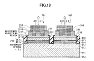
- the wavelength adjustment region includes the second phase adjustment layer 117 , the contact layer 118 , the first phase adjustment layer 121 and the wavelength adjustment layer 122 .
- the second phase adjustment layer 117 is formed of p-Al 0.1 Ga 0.9 As having an optical thickness of 0.05 ⁇ .
- the contact layer 118 is formed of p ++ GaAs having an optical thickness of 0.1 ⁇ .
- the first phase adjustment layer 121 is formed of GaInP having an optical thickness of about ⁇ /2.
- the wavelength adjustment layer 122 includes three layers in total of GaAsP/GaInP/GaAsP.
- the change in the optical thickness of the part of the wavelength adjustment region above the contact layer 118 between the case where the wavelength adjustment layer 122 is not etched and the case where all the layers of the wavelength adjustment layer 122 are etched decreases. Accordingly, the laser characteristics for the respective surface emitting lasers, such as the oscillation threshold electric current value or the slope efficiency can be made further uniform.
- the semiconductor layer may be formed by using the MOCVD method or the MBE method.
- the wavelength adjustment region is formed so that the layer numbers of the wavelength adjustment layers are made different for the respective surface emitting lasers by photolithography and selective etching, and the thicknesses of the layers are different.
- wet etching for example, for an etchant for GaAsF (the same for GaAs) a mixed liquid of sulfuric acid, hydrogen peroxide and water may be used.
- an etchant for GaInP a mixed liquid of hydrochloric acid and water may be used.
- the wavelength adjustment region is removed.
- the wavelength adjustment layer directly contacts the upper electrode or the like, materials to be contacted are different for the respective surface emitting lasers, and contact resistances are different. Moreover, depending on the thickness of the wavelength adjustment region, the amounts of electric current that can be applied to the respective surface emitting lasers are different. Accordingly, the electric characteristics and the emission characteristics for the respective surface emitting lasers differ substantially. Moreover, in the case of applying a current to the wavelength adjustment region, the electric resistance increases due to the band discontinuities on interfaces between the respective layers.
- the optical thickness of the first phase adjustment layer 221 is approximately ⁇ /2 so that a distance from a center of the contact layer 219 to a center of the fourth layer (GaInP) from the top in the wavelength adjustment layer 225 corresponds to an optical thickness of 3 ⁇ /4.
- the optical thickness of a part of the wavelength adjustment region above the contact layer 219 when all the layers of the wavelength adjustment layer 225 are etched is changed from the optical thickness where the wavelength adjustment layer 225 is not etched by 41%, which is relatively small. Accordingly, the laser characteristics for the respective surface emitting lasers, such as the oscillation threshold electric current value or the slope efficiency, can be made largely uniform.
- FIG. 16 illustrates a top view of the surface emitting laser element according to the present embodiment.
- the surface emitting laser element as an example, four surface emitting lasers capable of emitting light 381 , 382 , 383 and 384 are formed on a chip of 300 ⁇ m square.
- an upper electrode 361 of the surface emitting laser 381 is connected to an electrode pad 391
- an upper electrode 361 of the surface emitting laser 382 is connected to an electrode pad 392 .
- An upper electrode 361 of the surface emitting laser 383 is connected to an electrode pad 393
- an upper electrode 361 of the surface emitting laser 384 is connected to an electrode pad 394 .
- optical thickness of each of the three layers in total of p-GaAsP/p-GaInP/p-GaAsP in the wavelength adjustment layer 342 is 0.06 ⁇ , and the wavelength adjustment layer 342 is formed so that an interval of the oscillation wavelengths of the four surface emitting lasers is 2 nm.
- optical thicknesses of two kinds of materials p-Al 0.1 Ga 0.9 As and p-GaInP included in the second phase adjustment layer 218 and the first phase adjustment layer 341 are 0.03 ⁇ and 0.6 ⁇ , respectively.
Landscapes
- Physics & Mathematics (AREA)
- Condensed Matter Physics & Semiconductors (AREA)
- General Physics & Mathematics (AREA)
- Electromagnetism (AREA)
- Optics & Photonics (AREA)
- Spectroscopy & Molecular Physics (AREA)
- Semiconductor Lasers (AREA)
Applications Claiming Priority (4)
| Application Number | Priority Date | Filing Date | Title |
|---|---|---|---|
| JP2013-114881 | 2013-05-31 | ||
| JP2013114881 | 2013-05-31 | ||
| JP2014050392A JP2015008271A (ja) | 2013-05-31 | 2014-03-13 | 面発光レーザ素子及び原子発振器 |
| JP2014-050392 | 2014-03-13 |
Publications (2)
| Publication Number | Publication Date |
|---|---|
| US20140354366A1 US20140354366A1 (en) | 2014-12-04 |
| US9225149B2 true US9225149B2 (en) | 2015-12-29 |
Family
ID=50828755
Family Applications (1)
| Application Number | Title | Priority Date | Filing Date |
|---|---|---|---|
| US14/289,792 Expired - Fee Related US9225149B2 (en) | 2013-05-31 | 2014-05-29 | Surface emitting laser element and atomic oscillator |
Country Status (3)
| Country | Link |
|---|---|
| US (1) | US9225149B2 (de) |
| EP (1) | EP2808958A3 (de) |
| JP (1) | JP2015008271A (de) |
Cited By (2)
| Publication number | Priority date | Publication date | Assignee | Title |
|---|---|---|---|---|
| US20170025820A1 (en) * | 2014-03-14 | 2017-01-26 | Ricoh Company, Ltd. | Surface emitting laser, surface emitting laser element and atomic oscillator |
| US10170887B2 (en) | 2015-08-06 | 2019-01-01 | Ricoh Company, Ltd. | Surface emitting laser element and atomic oscillator |
Families Citing this family (10)
| Publication number | Priority date | Publication date | Assignee | Title |
|---|---|---|---|---|
| US10868407B2 (en) * | 2015-06-04 | 2020-12-15 | Hewlett Packard Enterprise Development Lp | Monolithic WDM VCSELS with spatially varying gain peak and fabry perot wavelength |
| DE102015114478A1 (de) * | 2015-08-31 | 2017-03-02 | Osram Opto Semiconductors Gmbh | Optoelektronischer Halbleiterchip und Verfahren zu dessen Herstellung |
| JP6862658B2 (ja) * | 2016-02-15 | 2021-04-21 | 株式会社リコー | 光増幅器、光増幅器の駆動方法及び光増幅方法 |
| US10516251B2 (en) * | 2016-06-28 | 2019-12-24 | Vi Systems Gmbh | Reliable high-speed oxide-confined vertical-cavity surface-emitting laser |
| TWI710187B (zh) * | 2017-02-09 | 2020-11-11 | 光環科技股份有限公司 | 垂直共振腔面射雷射結構及製法 |
| DE102017129173A1 (de) * | 2017-12-07 | 2019-06-13 | Osram Opto Semiconductors Gmbh | Strahlungsquelle zur Emission von Terahertz-Strahlung |
| JP7472468B2 (ja) * | 2019-03-20 | 2024-04-23 | 株式会社リコー | 照明装置、投影装置、計測装置、ロボット、電子機器、移動体、および造形装置 |
| US11527867B2 (en) | 2019-03-20 | 2022-12-13 | Ricoh Company, Ltd. | Surface emitting laser element, illumination device, projection device, measurement device, robot, electronic apparatus, mobile body, and modeling device |
| JP7434849B2 (ja) | 2019-11-29 | 2024-02-21 | 株式会社リコー | 面発光レーザ、面発光レーザ装置、光源装置及び検出装置 |
| US11876350B2 (en) * | 2020-11-13 | 2024-01-16 | Ii-Vi Delaware, Inc. | Multi-wavelength VCSEL array and method of fabrication |
Citations (22)
| Publication number | Priority date | Publication date | Assignee | Title |
|---|---|---|---|---|
| US5216686A (en) * | 1992-02-03 | 1993-06-01 | Motorola, Inc. | Integrated HBT and VCSEL structure and method of fabrication |
| US5493577A (en) * | 1994-12-21 | 1996-02-20 | Sandia Corporation | Efficient semiconductor light-emitting device and method |
| JP2751814B2 (ja) | 1994-01-14 | 1998-05-18 | 日本電気株式会社 | 波長多重面型発光素子の作製方法 |
| JPH11330631A (ja) | 1998-04-10 | 1999-11-30 | Hewlett Packard Co <Hp> | 垂直空洞面発光レ―ザ層構造、垂直空洞面発光レ―ザ・アレイ及び垂直空洞面発光レ―ザ・アレイの組立方法 |
| JP2000058958A (ja) | 1998-08-06 | 2000-02-25 | Nippon Telegr & Teleph Corp <Ntt> | 多波長面発光半導体レーザアレイ |
| US6195485B1 (en) | 1998-10-26 | 2001-02-27 | The Regents Of The University Of California | Direct-coupled multimode WDM optical data links with monolithically-integrated multiple-channel VCSEL and photodetector |
| US20010050934A1 (en) * | 2000-05-31 | 2001-12-13 | Choquette Kent D. | Long wavelength vertical cavity surface emitting laser |
| US20020085610A1 (en) * | 2000-12-29 | 2002-07-04 | Morgan Robert A. | Spatially modulated reflector for an optoelectronic device |
| US6566688B1 (en) * | 1998-12-03 | 2003-05-20 | Arizona Board Of Regents | Compound semiconductor structures for optoelectronic devices |
| US20050147143A1 (en) * | 2003-11-27 | 2005-07-07 | Naoto Jikutani | Surface-emission laser diode and surface-emission laser array, optical interconnection system, optical communication system, electrophotographic system, and optical disk system |
| JP2008053353A (ja) | 2006-08-23 | 2008-03-06 | Ricoh Co Ltd | 面発光レーザアレイ、それに用いられる面発光レーザ素子および面発光レーザアレイの製造方法 |
| US7453096B2 (en) * | 2001-03-27 | 2008-11-18 | Ricoh Company, Ltd. | Method of fabricating a semiconductor light-emitting device |
| JP2008283129A (ja) | 2007-05-14 | 2008-11-20 | Sony Corp | 面発光半導体レーザアレイ |
| JP2009188598A (ja) | 2008-02-05 | 2009-08-20 | Epson Toyocom Corp | 光学系及び原子発振器 |
| US7590159B2 (en) * | 2001-02-26 | 2009-09-15 | Ricoh Company, Ltd. | Surface-emission laser diode operable in the wavelength band of 1.1-1.7 micrometers and optical telecommunication system using such a laser diode |
| US8279519B2 (en) * | 2001-03-13 | 2012-10-02 | Ricoh Company, Ltd. | Semiconductor optical modulator, an optical amplifier and an integrated semiconductor light-emitting device |
| WO2013005813A1 (en) | 2011-07-07 | 2013-01-10 | Ricoh Company, Ltd. | Surface emitting laser element and atomic oscillator |
| US20130070039A1 (en) * | 2010-05-25 | 2013-03-21 | Kazuhiro Harasaka | Surface-emitting laser device, surface-emitting laser array, optical scanner, image forming apparatus, and method for manufacturing surface-emitting laser device |
| WO2013081176A1 (en) | 2011-12-02 | 2013-06-06 | Ricoh Company, Ltd. | Surface-emitting laser element, method for manufacturing a surface-emitting laser element, and atomic oscillator |
| US20130335155A1 (en) | 2011-03-17 | 2013-12-19 | Ricoh Company Ltd | Surface-emitting laser element, atomic oscillator, and surface-emitting laser element testing method |
| US20140023104A1 (en) | 2012-07-23 | 2014-01-23 | Ricoh Company, Ltd | Surface emitting laser device and atomic oscillator |
| US8705585B2 (en) | 2006-08-23 | 2014-04-22 | Ricoh Company, Ltd. | Surface-emitting laser array, optical scanning device, and image forming device |
-
2014
- 2014-03-13 JP JP2014050392A patent/JP2015008271A/ja active Pending
- 2014-05-28 EP EP20140170377 patent/EP2808958A3/de not_active Withdrawn
- 2014-05-29 US US14/289,792 patent/US9225149B2/en not_active Expired - Fee Related
Patent Citations (26)
| Publication number | Priority date | Publication date | Assignee | Title |
|---|---|---|---|---|
| US5216686A (en) * | 1992-02-03 | 1993-06-01 | Motorola, Inc. | Integrated HBT and VCSEL structure and method of fabrication |
| JP2751814B2 (ja) | 1994-01-14 | 1998-05-18 | 日本電気株式会社 | 波長多重面型発光素子の作製方法 |
| US5493577A (en) * | 1994-12-21 | 1996-02-20 | Sandia Corporation | Efficient semiconductor light-emitting device and method |
| JPH11330631A (ja) | 1998-04-10 | 1999-11-30 | Hewlett Packard Co <Hp> | 垂直空洞面発光レ―ザ層構造、垂直空洞面発光レ―ザ・アレイ及び垂直空洞面発光レ―ザ・アレイの組立方法 |
| US6259121B1 (en) | 1998-04-10 | 2001-07-10 | Agilent Technologies, Inc. | Monolithic multiple wavelength VCSEL array |
| JP2000058958A (ja) | 1998-08-06 | 2000-02-25 | Nippon Telegr & Teleph Corp <Ntt> | 多波長面発光半導体レーザアレイ |
| US6195485B1 (en) | 1998-10-26 | 2001-02-27 | The Regents Of The University Of California | Direct-coupled multimode WDM optical data links with monolithically-integrated multiple-channel VCSEL and photodetector |
| US6566688B1 (en) * | 1998-12-03 | 2003-05-20 | Arizona Board Of Regents | Compound semiconductor structures for optoelectronic devices |
| US20010050934A1 (en) * | 2000-05-31 | 2001-12-13 | Choquette Kent D. | Long wavelength vertical cavity surface emitting laser |
| US20020085610A1 (en) * | 2000-12-29 | 2002-07-04 | Morgan Robert A. | Spatially modulated reflector for an optoelectronic device |
| US7590159B2 (en) * | 2001-02-26 | 2009-09-15 | Ricoh Company, Ltd. | Surface-emission laser diode operable in the wavelength band of 1.1-1.7 micrometers and optical telecommunication system using such a laser diode |
| US8279519B2 (en) * | 2001-03-13 | 2012-10-02 | Ricoh Company, Ltd. | Semiconductor optical modulator, an optical amplifier and an integrated semiconductor light-emitting device |
| US7453096B2 (en) * | 2001-03-27 | 2008-11-18 | Ricoh Company, Ltd. | Method of fabricating a semiconductor light-emitting device |
| US20050147143A1 (en) * | 2003-11-27 | 2005-07-07 | Naoto Jikutani | Surface-emission laser diode and surface-emission laser array, optical interconnection system, optical communication system, electrophotographic system, and optical disk system |
| US8705585B2 (en) | 2006-08-23 | 2014-04-22 | Ricoh Company, Ltd. | Surface-emitting laser array, optical scanning device, and image forming device |
| JP2008053353A (ja) | 2006-08-23 | 2008-03-06 | Ricoh Co Ltd | 面発光レーザアレイ、それに用いられる面発光レーザ素子および面発光レーザアレイの製造方法 |
| JP2008283129A (ja) | 2007-05-14 | 2008-11-20 | Sony Corp | 面発光半導体レーザアレイ |
| JP2009188598A (ja) | 2008-02-05 | 2009-08-20 | Epson Toyocom Corp | 光学系及び原子発振器 |
| US20130070039A1 (en) * | 2010-05-25 | 2013-03-21 | Kazuhiro Harasaka | Surface-emitting laser device, surface-emitting laser array, optical scanner, image forming apparatus, and method for manufacturing surface-emitting laser device |
| US20130335155A1 (en) | 2011-03-17 | 2013-12-19 | Ricoh Company Ltd | Surface-emitting laser element, atomic oscillator, and surface-emitting laser element testing method |
| WO2013005813A1 (en) | 2011-07-07 | 2013-01-10 | Ricoh Company, Ltd. | Surface emitting laser element and atomic oscillator |
| US20140133510A1 (en) | 2011-07-07 | 2014-05-15 | Ricoh Company, Ltd. | Surface emitting laser element and atomic oscillator |
| WO2013081176A1 (en) | 2011-12-02 | 2013-06-06 | Ricoh Company, Ltd. | Surface-emitting laser element, method for manufacturing a surface-emitting laser element, and atomic oscillator |
| EP2690725A2 (de) | 2012-07-23 | 2014-01-29 | Ricoh Company, Ltd. | Oberflächenemittierende Laservorrichtung und Atomoszillator |
| US20140023104A1 (en) | 2012-07-23 | 2014-01-23 | Ricoh Company, Ltd | Surface emitting laser device and atomic oscillator |
| US8971372B2 (en) * | 2012-07-23 | 2015-03-03 | Ricoh Company, Ltd. | Surface emitting laser device and atomic oscillator |
Non-Patent Citations (8)
| Title |
|---|
| Apr. 17, 2015 European official action dated in corresponding European Patent Application No. 14 17 0377. |
| Darwin K. Serkland et al., "VCSELs for Atomic Clocks", Proc. of SPIE, vol. 6132, 613208 (2006). |
| Jean-Francois P. Seurin et al., "Modal competition in implant-apertured index-guided vertical-cavity surface-emitting lasers", Applied Physics Letters, vol. 77, pp. 3686-3688 (2000). |
| Padullaparthi Babu Dayal et al., "Multiple-Wavelength Vertical-Cavity Surface-Emitting Lasers by Grading a Spacer Layer for Short-Reach Wavelength Division Multiplexing Applications", Applied Physics Express 2, 092501 (2009). |
| Svenja Knappe et al., "A microfabricated atomic clock", Applied Physics Letters, vol. 85, pp. 1460-1462 (2004). |
| Svenja Knappe, "MEMS Atomic Clocks", Comprehensive Microsystems, vol. 3, pp. 571-612 (2007). |
| U.S. Appl. No. 14/069,541, filed Nov. 1, 2013. |
| Wupen Yuen et al. "Multiple-Wavelength Vertical-Cavity Surface-Emitting Laser Arrays with a Recorded Wavelength Span", IEEE Photonics Technology Letters, vol. 8, No. 1, Jan. 1, 1996, pp. 4-6. |
Cited By (3)
| Publication number | Priority date | Publication date | Assignee | Title |
|---|---|---|---|---|
| US20170025820A1 (en) * | 2014-03-14 | 2017-01-26 | Ricoh Company, Ltd. | Surface emitting laser, surface emitting laser element and atomic oscillator |
| US10084286B2 (en) * | 2014-03-14 | 2018-09-25 | Ricoh Company, Ltd. | Surface emitting laser, surface emitting laser element and atomic oscillator |
| US10170887B2 (en) | 2015-08-06 | 2019-01-01 | Ricoh Company, Ltd. | Surface emitting laser element and atomic oscillator |
Also Published As
| Publication number | Publication date |
|---|---|
| US20140354366A1 (en) | 2014-12-04 |
| EP2808958A3 (de) | 2015-05-20 |
| JP2015008271A (ja) | 2015-01-15 |
| EP2808958A2 (de) | 2014-12-03 |
Similar Documents
| Publication | Publication Date | Title |
|---|---|---|
| US9225149B2 (en) | Surface emitting laser element and atomic oscillator | |
| JP6303255B2 (ja) | 面発光レーザ素子及び原子発振器 | |
| US8971372B2 (en) | Surface emitting laser device and atomic oscillator | |
| EP2686923B1 (de) | Oberflächenemittierendes laserelement, atomoszillator und testverfahren für das oberflächenemittierende laserelement | |
| US9287682B2 (en) | Surface emitting laser device and atomic oscillator | |
| US10084286B2 (en) | Surface emitting laser, surface emitting laser element and atomic oscillator | |
| CN103650264A (zh) | 面发射激光器元件和原子振荡器 | |
| EP3128628B1 (de) | Oberflächenemittierendes laserelement und atomoszillator | |
| JP2017204616A (ja) | 面発光レーザ素子、原子発振器 | |
| JP2018073931A (ja) | 面発光レーザ素子、原子発振器 | |
| JP2014022667A (ja) | 面発光レーザ素子及び原子発振器 | |
| JP6699341B2 (ja) | 面発光レーザ素子、及びその製造方法、並びに原子発振器 | |
| JP2018010940A (ja) | 面発光レーザ素子及び原子発振器 | |
| JP6852262B2 (ja) | 面発光レーザ素子及び原子発振器 | |
| JP2016208049A (ja) | 面発光レーザ素子、原子発振器及び面発光レーザ素子の検査方法 |
Legal Events
| Date | Code | Title | Description |
|---|---|---|---|
| AS | Assignment |
Owner name: RICOH COMPANY, LTD., JAPAN Free format text: ASSIGNMENT OF ASSIGNORS INTEREST;ASSIGNORS:SUZUKI, RYOICHIRO;SATO, SHUNICHI;REEL/FRAME:032989/0139 Effective date: 20140526 |
|
| FEPP | Fee payment procedure |
Free format text: PAYOR NUMBER ASSIGNED (ORIGINAL EVENT CODE: ASPN); ENTITY STATUS OF PATENT OWNER: LARGE ENTITY |
|
| STCF | Information on status: patent grant |
Free format text: PATENTED CASE |
|
| FEPP | Fee payment procedure |
Free format text: MAINTENANCE FEE REMINDER MAILED (ORIGINAL EVENT CODE: REM.); ENTITY STATUS OF PATENT OWNER: LARGE ENTITY |
|
| LAPS | Lapse for failure to pay maintenance fees |
Free format text: PATENT EXPIRED FOR FAILURE TO PAY MAINTENANCE FEES (ORIGINAL EVENT CODE: EXP.); ENTITY STATUS OF PATENT OWNER: LARGE ENTITY |
|
| STCH | Information on status: patent discontinuation |
Free format text: PATENT EXPIRED DUE TO NONPAYMENT OF MAINTENANCE FEES UNDER 37 CFR 1.362 |
|
| FP | Lapsed due to failure to pay maintenance fee |
Effective date: 20191229 |