US9330883B2 - Charged particle beam device - Google Patents
Charged particle beam device Download PDFInfo
- Publication number
- US9330883B2 US9330883B2 US14/382,165 US201314382165A US9330883B2 US 9330883 B2 US9330883 B2 US 9330883B2 US 201314382165 A US201314382165 A US 201314382165A US 9330883 B2 US9330883 B2 US 9330883B2
- Authority
- US
- United States
- Prior art keywords
- sample
- contact probe
- charged particle
- particle beam
- absorption current
- Prior art date
- Legal status (The legal status is an assumption and is not a legal conclusion. Google has not performed a legal analysis and makes no representation as to the accuracy of the status listed.)
- Expired - Fee Related
Links
Images




Classifications
-
- H—ELECTRICITY
- H01—ELECTRIC ELEMENTS
- H01J—ELECTRIC DISCHARGE TUBES OR DISCHARGE LAMPS
- H01J37/00—Discharge tubes with provision for introducing objects or material to be exposed to the discharge, e.g. for the purpose of examination or processing thereof
- H01J37/02—Details
- H01J37/244—Detectors; Associated components or circuits therefor
-
- H—ELECTRICITY
- H01—ELECTRIC ELEMENTS
- H01J—ELECTRIC DISCHARGE TUBES OR DISCHARGE LAMPS
- H01J37/00—Discharge tubes with provision for introducing objects or material to be exposed to the discharge, e.g. for the purpose of examination or processing thereof
- H01J37/26—Electron or ion microscopes; Electron or ion diffraction tubes
- H01J37/28—Electron or ion microscopes; Electron or ion diffraction tubes with scanning beams
-
- H—ELECTRICITY
- H01—ELECTRIC ELEMENTS
- H01J—ELECTRIC DISCHARGE TUBES OR DISCHARGE LAMPS
- H01J37/00—Discharge tubes with provision for introducing objects or material to be exposed to the discharge, e.g. for the purpose of examination or processing thereof
- H01J37/30—Electron-beam or ion-beam tubes for localised treatment of objects
- H01J37/305—Electron-beam or ion-beam tubes for localised treatment of objects for casting, melting, evaporating, or etching
- H01J37/3053—Electron-beam or ion-beam tubes for localised treatment of objects for casting, melting, evaporating, or etching for evaporating or etching
- H01J37/3056—Electron-beam or ion-beam tubes for localised treatment of objects for casting, melting, evaporating, or etching for evaporating or etching for microworking, e. g. etching of gratings or trimming of electrical components
-
- H—ELECTRICITY
- H01—ELECTRIC ELEMENTS
- H01J—ELECTRIC DISCHARGE TUBES OR DISCHARGE LAMPS
- H01J37/00—Discharge tubes with provision for introducing objects or material to be exposed to the discharge, e.g. for the purpose of examination or processing thereof
- H01J37/30—Electron-beam or ion-beam tubes for localised treatment of objects
- H01J37/317—Electron-beam or ion-beam tubes for localised treatment of objects for changing properties of the objects or for applying thin layers thereon, e.g. for ion implantation
- H01J37/3178—Electron-beam or ion-beam tubes for localised treatment of objects for changing properties of the objects or for applying thin layers thereon, e.g. for ion implantation for applying thin layers on objects
-
- H—ELECTRICITY
- H01—ELECTRIC ELEMENTS
- H01J—ELECTRIC DISCHARGE TUBES OR DISCHARGE LAMPS
- H01J2237/00—Discharge tubes exposing object to beam, e.g. for analysis treatment, etching, imaging
- H01J2237/244—Detection characterized by the detecting means
-
- H—ELECTRICITY
- H01—ELECTRIC ELEMENTS
- H01J—ELECTRIC DISCHARGE TUBES OR DISCHARGE LAMPS
- H01J2237/00—Discharge tubes exposing object to beam, e.g. for analysis treatment, etching, imaging
- H01J2237/244—Detection characterized by the detecting means
- H01J2237/24495—Signal processing, e.g. mixing of two or more signals
-
- H—ELECTRICITY
- H01—ELECTRIC ELEMENTS
- H01J—ELECTRIC DISCHARGE TUBES OR DISCHARGE LAMPS
- H01J2237/00—Discharge tubes exposing object to beam, e.g. for analysis treatment, etching, imaging
- H01J2237/245—Detection characterised by the variable being measured
- H01J2237/24571—Measurements of non-electric or non-magnetic variables
Definitions
- the present invention relates to a charged particle beam device that irradiates a sample with a charged particle beam.
- charged particle beam devices such as a scanning electron microscope (SEM), a transmission electron microscope (TEM), a scanning transmission electron microscope (STEM), a focused ion beam (FIB) processing and observation system have been used to observe minute regions.
- SEM scanning electron microscope
- TEM transmission electron microscope
- STEM scanning transmission electron microscope
- FIB focused ion beam
- a sample is irradiated with a charged particle beam such as an electron beam and an ion beam.
- secondary electrons, reflection electrons, etc. are emitted from the front surface of the sample and transmission electrons are emitted from the rear surface thereof.
- an emission amount of these electrons i.e., charged particles
- an emission amount of these electrons has angular dependence so that the emission amount thereof changes associated with an emission angle, as depending on a shape and a composition, etc., of the sample. Accordingly, a device which detects those electrons at the most suitable angle has been proposed in case an emission amount of electrons has angular dependence (see Patent Literature 1, etc.).
- Patent Literature 1 JP 2010-199002 A
- reflection electrons have a large emission amount (i.e., strong signal intensity) in a specular reflection direction, while in a direction opposite to the specular reflection direction, reflection electrons in turn have a small emission amount and thereby the signal intensity is small. Therefore, based on the difference in those emission amounts, an image having different outline shades at the concave and convex parts may be acquired.
- the composition data of a sample is emphasized when two kinds of signal intensity, i.e., the strong signal intensity and the weak signal intensity are added together, whereas the concave and convex data of the sample are emphasized when they are subtracted one from the other.
- the emission amount (signal intensity) of the reflection electrons is acquired from the same sample, the different data is acquired depending on the emission angle, i.e., the detection angle of the reflection electrons.
- the emission angle i.e., the detection angle of the reflection electrons. The same applies not only to the reflection electrons but to secondary electrons and transmission electrons and also applies not only to electrons but to charged particles containing ions.
- an emission amount of reflection charged particles, secondary charged particles, or transmission charged particles, etc. has the angular dependence. Accordingly, development of a device capable of detecting charged particles at the most suitable angle in case an emission amount of the charged particles has angular dependence may meet a wide range of demands of the present age.
- a sample irradiated with a charged particle beam has a minute internal structure like, for example, a semiconductor device. Therefore, when only a local part constituting the minute structure is irradiated with a charged particle beam to detect charged particles emitted from the local part, the detection amount is small.
- a detector in order to detect the small amount of the charged particles, i.e., in order to increase sensitivity, it is desirable to arrange a detector as close to the sample as possible. This is because if charged particles fly a long distance, the charged particles are likely to be scattered and the collection efficiency of the charged particles becomes lower, even though the charged particles fly in a vacuum space.
- Patent Literature 1 describes that a detector is arranged closer to away from a sample to detect electrons of which emission amount has angular dependence at a most-suitable angle.
- the literature does not describe any of a device capable of increasing angle resolution of a detector even if the detector is arranged close to the sample.
- an object of the present invention is to provide a charged particle beam device having high sensitivity, which is capable of detecting charged particles emitted from a sample at a specific emission angle in a highly resolutional manner.
- the present invention provides a charged particle beam device comprising a charged particle beam irradiation unit that irradiates a sample with a charged particle beam, and an absorption current detector that detects an adsorption current generated in the sample by the irradiated charged particle beam.
- the absorption current detector detects the adsorption current thus generated in the sample and flowing through the detector, if the detector is arranged to contact with the sample.
- the charged particle beam device scans the sample with the charged particle beam to acquire an absorption current image.
- the absorption current detector detects, as the charged particle beam emitted from the sample by the irradiation of the charged particle beam is incident on the absorption current detector, the incident charged particle beam as a signal current dependent on an angle formed in a direction from an irradiation position of the charged particle beam on the sample toward the absorption current detector relative to at least one of a normal line direction of a front surface of the sample and an incident direction of the charged particle beam.
- a charged particle beam device having high sensitivity and capable of detecting charged particles emitted from a sample at a specific emission angle in a highly resolutional manner.
- FIG. 1 is a configuration view of a charged particle beam device according to a first embodiment of the present invention
- FIG. 2A is a schematic view showing a (first) method for detecting charged particles of which emission amount has angular dependence with the tip end of an absorption current detector in the charged particle beam device according to the first embodiment of the present invention
- FIG. 2B is a schematic view showing a method for detecting an absorption current from a sample with the tip end of the absorption current detector in the charged particle beam device according to the first embodiment of the present invention
- FIG. 2C is a schematic view showing a (second) method for detecting charged particles of which emission amount has angular dependence with the tip end of the absorption current detector in the charged particle beam device according to the first embodiment of the present invention
- FIG. 2D is a schematic view showing a (third) method for detecting charged particles of which emission amount has angular dependence with the tip end of the absorption current detector in the charged particle beam device according to the first embodiment of the present invention
- FIG. 2E is a schematic view showing a (fourth) method for detecting charged particles of which emission amount has angular dependence with the tip end of the absorption current detector in the charged particle beam device according to the first embodiment of the present invention
- FIG. 3 is a flowchart of a method for generating an image of charged particles of which emission amount has angular dependence with the charged particle beam device according to the first embodiment of the present invention
- FIG. 4 shows a GUI screen (first window, homepage) displayed on the display unit of the charged particle beam device according to the first embodiment of the present invention
- FIG. 5A shows a (first) detector status indication inside the GUI screen
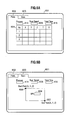
- FIG. 5B shows a (second) detector status indication inside the GUI screen
- FIG. 5C shows a (third) detector status indication inside the GUI screen
- FIG. 6A shows a GUI screen ((first) sequential acquisition setting screen) displayed on the display unit of the charged particle beam device according to the first embodiment of the present invention
- FIG. 6B shows a GUI screen ((second) sequential acquisition setting screen) displayed on the display unit of the charged particle beam device according to the first embodiment of the present invention
- FIG. 7 shows a configuration view of the charged particle beam device according to a second embodiment of the present invention.
- FIG. 8 is a schematic view showing a method for forming a non-contact probe in a base material with the charged particle beam device according to the second embodiment of the present invention.
- FIG. 9 is a plane view of the base material in which the plurality of non-contact probes is formed.
- FIG. 1 shows a configuration view of a charged particle beam device 1 according to a first embodiment of the present invention.
- the first embodiment exemplifies an SEM, i.e., an electron beam device as the charged particle beam device 1
- the present invention can also be applied to other charged particle beam devices (charged particle beam microscopes) 1 .
- the charged particle beam device 1 has: a sample stage 102 that has a sample 101 placed thereon and causes the same to move, a sample position control unit 103 that controls the movement, etc., of the sample stage 102 ; an electron beam optical system unit 105 that irradiates the sample 101 with an electron beam (charged particle beam) 104 for scanning; an electron beam optical system control unit 106 that controls the electron beam optical system unit 105 ; a secondary electron detector 107 that detects secondary electrons, etc., generated from the sample 101 ; a secondary electron detector control unit 108 that controls the secondary electron detector 107 ; a conductive member 109 ; an absorption current detector 110 that has the conductive member 109 detachably mounted on the tip end thereof and detects an absorption current; an absorption current detector control unit 111 that controls the detection of the absorption current detector 110 ; an absorption current detector stage 112 that has the absorption current detector 110 placed thereon and causes the same to move; an absorption current detector position control unit 113 that controls the movement of
- the sample position control unit 103 , the electron beam optical system control unit 106 , the secondary electron detector control unit 108 , the absorption current detector control unit 111 , and the absorption current detector position control unit 113 , etc., are controlled by the central processing unit 114 .
- the central processing unit 114 a personal computer, a workstation, etc., can be, for example, used.
- the sample stage 102 , the electron beam optical system unit 105 , the secondary electron detector 107 , the absorption current detector 110 , and the absorption current detector stage 112 are arranged in the vacuum container 116 .
- the sample 101 is irradiated with the electron beam 104 , and secondary electrons, etc., of which emission amount has angular dependence among the secondary electrons, etc., emitted from the sample 101 are taken by the conductive member 109 to generate a signal current.
- the absorption current detector 110 detects the signal current as an absorption current and acquires a signal current image as is the case with an absorption current image.
- the conductive member 109 is mounted on a cable-like tip end 202 of the absorption current detector 110 .
- the conductive member 109 can be arranged near the sample 101 , and even a slight amount of the secondary electrons emitted from the sample 101 can be reliably taken.
- the conductive member 109 is arranged in a specific direction providing angular dependence relative to the sample 101 .
- the signal current described above can be acquired.
- a signal current image can be acquired when the signal current described above is acquired while the electron beam 104 for the irradiation of the sample 101 is scanned.
- the secondary electrons, etc., emitted from the sample 101 can also be detected by the secondary electron detector 107 .
- An SEM image can be acquired when the secondary electrons, etc., are detected by the secondary electron detector 107 while the electron beam 104 for the irradiation of the sample 101 is scanned.
- FIG. 2A shows a (first) method for detecting secondary charged particles (secondary electrons) 201 of which emission amount has angular dependence with the tip end 202 of the absorption current detector 110 in the charged particle beam device 1 according to the first embodiment of the present invention.
- the secondary charged particles (secondary electrons) include secondary charged particles (reflection electrons).
- a signal current Ia flows from the conductive member 109 to a signal line 204 connected to the conductive member 109 .
- all the secondary electrons 201 colliding with the conductive member 109 are not necessarily converted into the signal current Ia but the difference between the secondary electrons 201 colliding with the conductive member 109 and tertiary charged particles (tertiary electrons) 205 emitted from the conductive member 109 is turned into the signal current Ia.
- the signal current Ia With the detection of the signal current Ia, it becomes possible to acquire a signal current image reflecting the sample data of the secondary electrons 201 .
- the signal current Ia is extremely weak, imaging can be achieved, for example, by increasing the current amount of the electron beam 104 or by increasing the signal amplification ratio of the absorption current detector 110 , etc.
- the conductive member 109 is arranged such that an angle ⁇ formed in a direction from the irradiation position of the electron beam 104 on the sample 101 toward the conductive member 109 relative to the normal line direction of the front surface of the sample or the incident direction of the electron beam 104 agrees with a specific angle at which the secondary electrons 201 of which emission amount has angular dependence are emitted.
- the conductive member 109 is arranged such that a range ⁇ of the angle at which the conductive member 109 is seen from the irradiation position of the electron beam 104 on the sample 101 agrees with the specific angle range at which the secondary electrons 201 of which emission amount has angular dependence are emitted.
- the tip end 202 of the absorption current detector 110 has a coaxial cable 203 , a contact probe 208 connected to the coaxial cable 203 , and the conductive member (non-contact probe) 109 connected to the contact probe 208 .
- the coaxial cable 203 has the signal line 204 through which the signal current Ia flows, a shield 207 that covers the signal line 204 and is grounded, and an insulation material 206 that insulates the signal line 204 from the shield 207 .
- the contact probe 208 protrudes from the end of the coaxial cable 203 .
- the contact probe 208 is connected to and supported by the signal line 204 . As will be described later, the contact probe 208 is used as a probe that is brought into contact with and is electrically connected to the sample 101 .
- the conductive member 109 is connected to and supported by the contact probe 208 . As shown in FIG. 2A , the conductive member 109 is used as a non-contact probe that is not brought into contact with the sample 101 . In this way, only the secondary electrons 201 colliding with the conductive member 109 can be turned into the signal current Ia. Since the shield 207 is grounded, the secondary electrons 201 colliding with the shield 207 flow to the ground, whereby the occurrence of a charge up can be prevented. Note that if the secondary electrons 201 colliding with the conductive member 109 are extremely greater in amount than the secondary electrons 201 colliding with the shield 207 , the shield 207 and the insulation material 206 can be omitted.
- the conductive member 109 is connected to the tip of the contact probe 208 and capable of being attached to and detached from the contact probe 208 .
- the contact probe 208 may also have the function of the conductive member 109
- the conductive member 109 may be omitted.
- the conductive member 109 is directly connected to the sample 10 without being detached from the contact probe 208
- the conductive member 109 may also have the function of the contact probe 208 . That is, the contact probe 208 that detects an absorption current may be used as the conductive member (non-contact probe) 109 to detect the signal current Ia.
- a probe that extracts a micro sample may be used as the conductive member (non-contact probe) 109 or the contact probe 208 in micro samplingTM.
- the conductive member 109 is formed in a disc shape in FIG. 2A , the shape of the conductive member 109 is not limited to it. By changing the shape, size, etc., of the conductive member 109 , detection sensitivity and a detection region can be changed.
- a method for changing the size and shape of the conductive member 109 includes a method for replacing the conductive member 109 with another member having a different size and shape as will be described later, a method for rotating or reciprocating the conductive member 109 together with the tip end 202 of the absorption current detector 110 , etc.
- the material of the conductive member 109 is desirably a light element that emits a small amount of secondary electrons or contains the light element.
- the composition of the material of the conductive member 109 is desirably an element having a smaller atomic number than copper or contains the element. The composition can reduce the emission of the tertiary electrons 205 and increase the signal current Ia.
- the function of applying a voltage to the conductive member 109 may be provided.
- the conductive member 109 can attract secondary electrons, reflection electrons, tertiary electrons, etc., and increase the signal current Ia.
- a voltage of about ⁇ 50 V is applied to the conductive member 109 , the conductive member 109 can reject secondary electrons and acquire only reflection electrons.
- the angle ⁇ described above is deviated from the specific angle, at which the secondary electrons 201 of which emission amount has angular dependence are emitted, when the irradiation position on the sample is moved by the scanning of the electron beam 104 . Accordingly, first, with the unit image acquisition system of the central processing unit 114 , a region R 2 on the sample 101 satisfying the condition that the angle ⁇ substantially equals the specific angle is scanned by the electron beam 104 to acquire a unit image according to the signal current Ia.
- the detector movement system of the central processing unit 114 moves the tip end 202 (conductive member 109 ) of the absorption current detector from a position P 2 to a position P 3 satisfying the condition described above.
- the acquisition of a unit image and the movement of the tip end 202 (conductive member 109 ) of the absorption current detector described above are repeatedly performed.
- a plurality of unit images such as a unit image corresponding to a region R 1 and a position P 1 , a unit image corresponding to the region R 2 and the position P 2 , and a unit image corresponding to the region R 3 and the position P 3 can be acquired.
- the central processing unit 114 can acquire a signal current image.
- FIG. 2B shows a method for detecting an absorption current Ib from the sample 101 with the tip end 202 of the absorption current detector in the charged particle beam device according to the first embodiment of the present invention.
- the conductive member 109 is removed from the contact probe 208 .
- the contact probe 208 is brought into contact with the sample 101 .
- the absorption current Ib as well as the secondary electrons 201 is generated in the sample 101 .
- the absorption current Ib flows into the contact probe 208 and is detected by the absorption current detector 110 (see FIG. 1 ). Further, an absorption current image can be acquired when the electron beam 104 scans the sample 101 .
- FIG. 2C shows a (second) method for detecting charged particles of which emission amount has angular dependence with the tip end 202 of the absorption current detector in the charged particle beam device according to the first embodiment of the present invention.
- the contact probe 208 has a conductive member (probe for reflection electrons) 109 a ( 109 ) mounted on the tip thereof.
- the conductive member 109 a is formed in a substantially horseshoe shape.
- the outer circumference of the conductive member 109 a is formed in a semi-circular shape, and the inner circumference thereof is also formed in a semi-circular shape concentric with the semi-circular shape of the outer circumference.
- the secondary electrons 201 of which emission amount has the angular dependence of the same properties are emitted together with reflection electrons along the cone-like side surface of a downward convexity whose apex is located at an irradiation position on the sample 101 . Accordingly, if the conductive member 109 a is arranged along the circumferential direction of the cone, the yield of the secondary electrons 201 can be increased. Further, if the conductive member 109 a is arranged closer to the sample 101 , the secondary electrons 201 , each of which forms a greater angle in the emitted direction thereof relative to the direction of the electron beam, can be taken.
- the secondary electrons 201 each of which forms a smaller angle in the emitted direction thereof relative to the direction of the electron beam, can be taken.
- the emission amount of the secondary electrons 201 may have angular dependence in the circumferential direction. Since the conductive member 109 a is arranged by 180° half the entire circumferential angle 360° in the circumferential direction, the secondary electrons 201 of which emission amount has angular dependence in the circumferential direction can also be detected.
- the conductive member 109 a is arranged on the same side as the electron beam 104 relative to the sample 101 , the outer circumference and the inner circumference are formed in the semi-circular shapes in the planar view of the conductive member 109 a . Therefore, the electron beam 104 can be easily taken in or taken out the conductive member 109 a without intersecting the conductive member 109 to perform scanning.
- FIG. 2D shows a (third) method for detecting charged particles of which emission amount has angular dependence with the tip end 202 of the absorption current detector in the charged particle beam device according to the first embodiment of the present invention.
- the contact probe 208 has a conductive member (probe for transmission electrons) 109 b ( 109 ) mounted on the tip thereof.
- the conductive member 109 b is formed in a ring shape.
- the outer circumference of the conductive member 109 b is formed in a circular shape, and the inner circumference thereof is also formed in a circular shape concentric with the circular shape of the outer circumference.
- the secondary electrons 201 pass through the sample 101 like transmission electrons besides being reflected like reflection electrons. Further, the secondary electrons 201 of which emission amount has the angular dependence of the same properties among the transmission electrons are emitted along the cone-like side surface of an upward convexity whose apex is located at an irradiation position on the sample 101 . Accordingly, if the conductive member 109 b is arranged along the circumferential direction of the cone, the yield of the secondary electrons (transmission electrons) 201 can be increased. Further, if the conductive member 109 b is arranged closer to the sample 101 , the secondary electrons 201 , each of which forms a greater angle in the emitted direction thereof relative to the direction of the electron beam, can be taken.
- the conductive member 109 b is arranged separated from the sample 101 , the secondary electrons 201 , each of which forms a smaller angle in the emitted direction thereof relative to the direction of the electron beam, can be taken. Note that the conductive member 109 b is arranged on a side opposite to the electron beam 104 relative to the sample 101 .
- FIG. 2E shows a (fourth) method for detecting charged particles of which emission amount has angular dependence with the tip end 202 of the absorption current detector in the charged particle beam device according to the first embodiment of the present invention.
- the contact probe 208 has a conductive member (probe for a diffraction pattern) 109 c ( 109 ) mounted on the tip thereof.
- the conductive member 109 c is formed in a rectangular shape. In a planar view, the conductive member 109 c is formed in a square shape.
- the conductive member 109 c is arranged on a side opposite to the electron beam 104 relative to the sample 101 .
- the square shape of the conductive member 109 c is made into a pixel at each position of the diffraction pattern.
- the conductive member 109 c is moved to scan a plane at which the diffraction pattern is generated, while the secondary electron (transmission electron) 201 is acquired for each position as the pixel of each position on the plane.
- the acquired secondary electron (transmission electron) 201 is detected for each position as the signal current Ia.
- the probe can be changed for different purposes in such a way that the contact probe 208 of FIG. 2B is used or the conductive member (probe for reflection electrons) 109 a of FIG. 2C , the conductive member (probe for transmission electrons) 109 b of FIG. 2D , or the conductive member (probe for a diffraction pattern) 109 c of FIG. 2E is mounted on the contact probe 208 instead of the conductive member 109 .
- FIG. 3 shows the flowchart of a method for generating an image of charged particles of which emission amount has angular dependence with the charged particle beam device according to the first embodiment of the present invention. Based on this, a signal current image can be sequentially acquired at a plurality of positions registered in advance.
- an operator places the sample 101 on the sample stage 102 extracted from the vacuum container 116 .
- the central processing unit 114 introduces the sample stage 102 having the sample 101 placed thereon into the vacuum container 116 via the sample position control unit 103 .
- step S 2 the central processing unit 114 controls the electron beam optical system unit via the electron beam optical system control unit to scan and irradiate the circumference of the sample 101 with the electron beam 104 and controls the secondary electron detector 107 via the secondary electron detector control unit 108 to detect secondary electrons emitted from the circumference of the sample 101 and display an SEM image on the display unit 115 . While confirming the SEM image, the operator controls the sample stage 102 and adjusts the position of the sample 101 from the central processing unit 114 .
- FIG. 4 shows a GUI screen (first window, homepage) 115 a displayed on the display unit 115 .
- the central processing unit 114 causes the display unit 115 to display the GUI screen (first window, homepage) 115 a .
- the operator instructs the central processing unit 114 to switch a using detector from the secondary electron detector 107 to the absorption current detector 110 with a detector selection pull-down menu 401 , and the central processing unit 114 switches to the using detector according to the instruction.
- step S 4 the central processing unit 114 controls the electron beam optical system unit via the electron beam optical system control unit to scan and irradiate the circumference of the sample 101 and the tip end 202 of the absorption current detector with the electron beam 104 and controls the secondary electron detector 107 via the secondary electron detector control unit 108 to detect secondary electrons emitted from the circumference of the sample 101 and the tip end 202 of the absorption current detector and display an SEM image on the display unit 115 .
- the central processing unit 114 controls the sample stage 102 to adjust the position of the sample 101 and controls the absorption current detector stage 112 to adjust the position of the conductive member 109 (contact probe 208 ) to introduce the conductive member 109 (contact probe 208 and absorption current detector 110 ) into the view of the SEM image.
- the central processing unit 114 withdraws the conductive member 109 (contact probe 208 and absorption current detector) outside the view of the SEM image.
- step S 5 the central processing unit 114 causes the display unit 115 to display the GUI screen (first window, homepage) 115 a shown in FIG. 4 .
- the operator selects the type of an angular dependence signal to be detected by the absorption current detector 110 with a detection signal (probe) selection pull-down menu 402 . That is, the operator selects a using probe from among the contact probe 208 , the probe 109 a for reflection electrons, the probe 109 b for transmission electrons, and the probe 109 c for a diffraction pattern.
- the operator instructs the central processing unit 114 to switch to the using probe, and the central processing unit 114 switches to the using probe according to the instruction.
- step S 6 the operator clicks a detector initial setting button indication 411 of FIG. 4 to perform initial settings.
- the central processing unit 114 performs, for example, the measurement of the shapes of the conductive member 109 and the sample 101 , the adjustment of a mutual positional relationship, a detection region, the avoidance of the interference between the conductive member 109 and the sample 101 , etc.
- the central processing apparatus 114 controls the electron beam optical system unit 105 via the electron beam optical system control unit 106 to scan and irradiate the circumference of the conductive member 109 and the sample 101 with the electron beam 104 and controls the secondary electron detector 107 via the secondary electron detector control unit 108 to detect secondary electrons emitted from the circumference of the conductive member 109 and the sample 101 and acquire the SEM image of the conductive member 109 and the sample 101 .
- the results of measuring the shapes and adjusting a detection region and the positional relationship between the conductive member 109 and the sample 101 are displayed on an X-Y plane indication 404 and an X-Z plane indication 405 of a detector status indication 403 of FIG. 4 .
- the operator can adjust the positions of the conductive member 109 and the sample 101 via the central processing unit 114 .
- the positional relationship between the conductive member 109 and the sample 101 is set such that the conductive member 109 and the sample 101 do not interfere with each other and secondary electrons of which emission amount has angular dependence are incident on the conductive member 109 .
- an absorption current image which is acquired by scanning and irradiating the conductive member 109 and its circumference with the electron beam 104 and detecting an absorption current generated by the irradiation from the conductive member 109 with the absorption current detector 110 , may be used instead of the SEM image described above. In this way, an image that does not reflect the sample 101 , etc., but reflects only the shape of the conductive member 109 can be acquired, which in turn improves measurement accuracy.
- a signal current image which is acquired by scanning and irradiating the sample 101 and its circumference with the electron beam 104 , acquiring secondary electrons emitted by the irradiation from the sample 101 with the conductive member 109 to generate a signal current, and detecting the signal current with the absorption current detector 110 , may be used instead of the SEM image described above.
- the adjustment of avoiding the interference with the sample 101 includes, for example, a method for once bringing the conductive member 109 into contact with the sample 101 to register a mutual position, a method for rotating the conductive member 109 to capture an image from the side surface and measuring and registering the distance between the conductive member and the sample 101 based on the image, etc.
- FIG. 5A shows a (first) example of the detector status indication 403 inside the GUI screen at initial settings.
- the X-Y plane indication 404 of the detector status indication 403 indicates an image 501 of the conductive member (probe for reflection electrons) 109 a projected on an X-Y plane.
- a position 503 at which the conductive member (probe for reflection electron) 109 a is supported by the contact probe 208 is indicated.
- the size or the like of the diameter of the semi-circle such as the outer circumference of the conductive member (probe for reflection electrons) 109 a is measured and indicated by a size indication 504 .
- the X-Z plane indication 405 of the detector status indication 403 indicates the image 501 of the conductive member (probe for reflection electrons) 109 a projected on an X-Z plane and an image 502 of the sample 101 projected on the X-Z plane.
- the size or the like of the distance between the conductive member (probe for reflection electrons) 109 a and the sample 101 is measured and indicated by a size indication 504 .
- FIG. 5B shows a (second) example of the detector status indication 403 inside the GUI screen at initial settings.
- the X-Y plane indication 404 of the detector status indication 403 indicates an image 501 of the conductive member (probe for transmission electrons) 109 b projected on the X-Y plane.
- a position 503 at which the conductive member (probe for transmission electrons) 109 b is supported by the contact probe 208 is indicated.
- the size or the like of the diameter of the circle such as the outer circumference of the conductive member (probe for transmission electrons) 109 b is measured and indicated by a size indication 504 .
- the X-Z plane indication 405 of the detector status indication 403 indicates the image 501 of the conductive member (probe for transmission electrons) 109 b projected on the X-Z plane and an image 502 of the sample 101 projected on the X-Z plane.
- the size or the like of the distance between the conductive member (probe for transmission electrons) 109 b and the sample 101 is measured and indicated by a size indication 504 .
- FIG. 5C shows a (third) example of the detector status indication 403 inside the GUI screen at initial settings.
- the X-Y plane indication 404 of the detector status indication 403 indicates an image 501 of the conductive member (probe for a diffraction pattern) 109 c projected on the X-Y plane.
- a position 503 at which the conductive member (probe for a diffraction pattern) 109 c is supported by the contact probe 208 is indicated.
- a scanning direction (range) indication 505 of the conductive member (probe for a diffraction pattern) 109 c is indicated.
- the X-Z plane indication 405 of the detector status indication 403 indicates the image 501 of the conductive member (probe for a diffraction pattern) 109 c projected on the X-Z plane and an image 502 of the sample 101 projected on the X-Z plane.
- the size or the like of the distance between the conductive member (probe for a diffraction pattern) 109 c and the sample 101 is measured and indicated by a size indication 504 .
- step S 7 of FIG. 3 the operator clicks a sequential acquisition setting button indication 413 of a sequential acquisition indication 412 of FIG. 4 to perform sequential image acquisition settings.
- the central processing unit 114 registers the coordinates of the driving position of the conductive member 109 and sets up the acquisition number and the observation conditions of a signal current image. Note that steps S 6 and S 7 can be omitted if previously-set conditions are used.
- FIG. 6A shows a GUI screen (sequential acquisition setting screen (first: coordinate position setting mode 602 )) 601 displayed on the display unit 115 when the sequential acquisition setting button indication 413 of FIG. 4 is clicked at sequential image acquisition settings.
- the coordinate position setting mode 602 a plurality of positions at the observation of the conductive member 109 , specifically, a plurality of moving destinations of the position 503 (see FIG. 5A , etc.) is set (registered) in a coordinate registration table indication 604 .
- the positions may be set with XYZ coordinates or may be set with T (angle) and R (distance).
- a process number indication 414 indicates the number of positions registered in the coordinate registration table indication 604 .
- an acquisition time setting indication 605 an acquisition time per one sheet (one area) can be set. The longer the acquisition time, the clearer image quality becomes.
- a total time is determined by the product of an image acquisition time indicated by the image acquisition time setting indication 605 and the number of processes indicated by the process number indication 414 and is indicated by a total time indication 415 .
- FIG. 6B shows a GUI screen (sequential acquisition setting screen (second: moving region setting mode 603 )) 601 displayed on the display unit 115 when the sequential acquisition setting button indication 413 of FIG. 4 is clicked at sequential image acquisition settings.
- a moving region setting mode 603 the scanning range of the electron beam 104 is determined by setting a start coordinate position setting indication 606 , an end coordinate position setting indication 607 , and a pixel number setting indication 608 .
- an image acquisition time indicated by an image acquisition time setting indication 605 and a total time indicated by a total time indication 415 are changed. While seeing the total time indication 415 , etc., the operator can change the number of pixels, etc., indicated by the pixel number setting indication 608 .
- step S 8 of FIG. 3 the operator clicks a moving button 417 of FIG. 4 to start sequential image acquisition.
- the sequential image acquisition can be stopped when a stop button 418 is clicked.
- the conductive member 109 and the sample 101 can be moved to the position initially set in step S 6 when a home position button 416 is clicked.
- step S 9 the central processing unit 114 moves the conductive member 109 (absorption current detector 110 ) to the coordinate position (registered coordinates) registered in step S 7 .
- a current coordinate indication 407 of a tip coordinate indication 406 of FIG. 4 indicates the current position of the conductive member 109 .
- a setting coordinate indication 408 of the tip coordinate indication 406 indicates registered coordinates corresponding to the current position. Since the current position indicated by the current coordinate indication 407 and the registered coordinates indicated by the setting coordinate indication 408 are indicated so as to be vertically arranged side by side, determination as to whether they agree with each other can be easily made. When they substantially agree with each other, it can be determined that the conductive member 109 is normally moved.
- step S 10 the central processing unit 114 acquires an absorption current image (or a unit image) for each of the registered coordinates.
- step S 11 the central processing unit 114 repeatedly performs the processing of steps S 9 and S 10 until the signal current image is acquired by the number (prescribed number) set in step S 7 .
- the flow is ended when the signal current image is acquired by the prescribed number.
- a mechanism capable of tilting the absorption current detector 110 may be provided for the movement of the absorption current detector 110 (conductive member 109 ).
- the absorption current detector 110 is also tilted so as to suit the sample 101 and a plane parallel to the front surface of the sample 101 is used as an X-Y driving surface, whereby a complicated operation requiring triaxial driving can be limited to an X-Y biaxial movement and the movement of the conductive member 109 is easily performed.
- a mechanism capable of rotating the conductive member 109 may be provided.
- the conductive member (probe for reflection electrons) 109 a shown in FIG. 2C can be moved in the circumferential direction, and angular dependence in the circumferential direction can be easily observed.
- FIG. 7 shows a configuration view of the charged particle beam device 1 according to a second embodiment of the present invention.
- the second embodiment is different from the first embodiment in that it has an ion beam optical system unit (ion beam irradiation unit) 702 that irradiates the sample 101 and the conductive member 109 with an ion beam 701 and has an assist gas supply unit 704 that supplies assist gas to the sample 101 and the conductive member 109 .
- ion beam optical system unit ion beam irradiation unit
- the ion beam optical system unit 702 and the assist gas supply unit 704 are arranged in the vacuum container 116 .
- the charged particle beam device 1 has an ion beam optical system control unit 703 that controls the ion beam optical system unit 702 and has an assist gas supply control unit 705 that controls the assist gas supply unit 704 .
- the ion beam optical system unit 702 can be operated by the central processing unit 114 via the ion beam optical system control unit 703 .
- the assist gas supply unit 704 can be operated by the central processing unit 114 via the assist gas supply control unit 705 .
- FIG. 8 shows a method for forming the conductive member (probe for reflection electrons) 109 a in a conductive base material 801 with the charged particle beam device 1 of the second embodiment.
- the ion beam optical system unit 702 applies a great acceleration voltage to irradiate the base material 801 with the ion beam 701 , the irradiated part can be etched (cut away). Therefore, first, a circumferential processing groove 802 is formed in the base material 801 by the etching described above.
- the circumferential processing groove 802 is formed in such a way as to leave the conductive member 109 a and a support portion 804 .
- bottom-cutting processing space 803 is formed between the conductive member 109 a (support portion 804 ) and the main body of the base material 801 .
- the conductive member 109 a is brought into a state of floating in the air while being supported by the support portion 804 .
- the contact probe 208 is brought into contact with the conductive member 109 a .
- an electric conductor 806 is deposited on the conductive member 109 a and the contact probe 208 , whereby the conductive member 109 a can be connected (joined) to the tip of the contact probe 208 .
- the second embodiment can use the charged particle beam 104 instead of the ion beam 701 if the charged particle beam 104 is not an electron beam but an ion beam.
- the ion beam optical system unit 702 for the irradiation of the ion beam 701 can be omitted.
- the support portion 804 is irradiated with the ion beam 701 to be etched and cut away.
- the conductive member 109 a can be extracted from the base material 801 in a state of being connected to the contact probe 208 . Note that the extraction can be performed in the same way as micro sampling (TM).
- the sample 101 may be used as the base material 801 or may be arranged near the sample 101 .
- the part of the sample 101 with which the contact probe 208 is brought into contact is only required to be irradiated with the ion beam 701 while the assist gas is supplied to the sample 101 in a state in which the contact probe 208 is brought into contact with the sample 101 .
- the electric conductor is deposited on the sample 101 and the contact probe 208 , whereby the sample 101 and the contact probe 208 can be connected (joined) to each other.
- FIG. 9 shows a plane view of the base material 801 in which the plurality of conductive members (non-contact probes) 109 ( 109 a , 109 b , 109 c , 109 d , and 109 e ) is formed.
- the base material 801 has the plurality of conductive members (probes for reflection electrons) 109 a , conductive members (probes for transmission electrons) 109 b , and conductive members (probes for a diffraction pattern) 109 c supported by the support portions 804 .
- the base material 801 has the plurality of conductive members (probes for reflection electrons) 109 d supported by the support portions 804 .
- the outer circumference of the conductive members 109 d is formed in a quarter-circular shape (fan shape), and the inner circumference thereof is also formed in a fan shape concentric with the fan shape of the outer circumference.
- the conductive members 109 d can observe angular dependence in the circumferential direction at higher resolution than the conductive members 109 a . Further, if the central angle of the fan shape is decreased, the resolution can be increased.
- the base material 801 has the plurality of conductive members (probes for transmission electrons) 109 e supported by the support portions 804 .
- the outer diameter and the inner diameter of the conductive members 109 e are smaller in size than those of the conductive members 109 b .
- the conductive members 109 e can be moved closer to the sample 101 than the conductive members 109 b if the same secondary electrons are detected, and can detect secondary electrons of which emission amount has angular dependence different from the angular dependence of the conductive members 109 b if a distance to the sample 101 is set to be the same between the conductive members 109 b and 109 e .
- the various conductive members (non-contact probes) 109 ( 109 a , 109 b , 109 c , 109 d , and 109 e ) can be quickly prepared (mounted).
- etching gas that performs etching with the irradiation of the electron beam 104 may be supplied, or deposition gas that is deposited with the irradiation of the electron beam 104 may be supplied.
- electron beam optical system unit charged particle beam irradiation unit
- electron beam optical system control unit charged particle beam irradiation unit
- conductive member non-contact probe: absorption current detector
- conductive member ((non-contact) probe for reflection (secondary) charged particles: absorption current detector)
- 109 b conductive member ((non-contact) probe for transmission charged particles: absorption current detector)
- 109 c conductive member ((non-contact) probe for diffraction pattern: absorption current detector)
- absorption current detector main body absorption current detector
- absorption current detector control unit absorption current detector
- absorption current detector stage detector moving unit: absorption current detector
- absorption current detector position control unit absorption current detector
- central processing unit unit image acquisition system, computer
- ion beam optical system unit ion beam irradiation unit
- ion beam optical system control unit ion beam irradiation unit
- ⁇ angle formed in direction from irradiation position of charged particle beam on sample toward emitting direction relative to incident direction
- R 1 , R 2 , R 3 scanning region on sample satisfying angle conditions
Landscapes
- Chemical & Material Sciences (AREA)
- Analytical Chemistry (AREA)
- Physics & Mathematics (AREA)
- Engineering & Computer Science (AREA)
- Plasma & Fusion (AREA)
- Analysing Materials By The Use Of Radiation (AREA)
Applications Claiming Priority (3)
| Application Number | Priority Date | Filing Date | Title |
|---|---|---|---|
| JP2012-045128 | 2012-03-01 | ||
| JP2012045128A JP5852474B2 (ja) | 2012-03-01 | 2012-03-01 | 荷電粒子線装置 |
| PCT/JP2013/054217 WO2013129209A1 (fr) | 2012-03-01 | 2013-02-20 | Dispositif à faisceau de particules chargées |
Publications (2)
| Publication Number | Publication Date |
|---|---|
| US20150014529A1 US20150014529A1 (en) | 2015-01-15 |
| US9330883B2 true US9330883B2 (en) | 2016-05-03 |
Family
ID=49082409
Family Applications (1)
| Application Number | Title | Priority Date | Filing Date |
|---|---|---|---|
| US14/382,165 Expired - Fee Related US9330883B2 (en) | 2012-03-01 | 2013-02-20 | Charged particle beam device |
Country Status (5)
| Country | Link |
|---|---|
| US (1) | US9330883B2 (fr) |
| JP (1) | JP5852474B2 (fr) |
| CN (1) | CN104126217B (fr) |
| DE (1) | DE112013000852B4 (fr) |
| WO (1) | WO2013129209A1 (fr) |
Cited By (1)
| Publication number | Priority date | Publication date | Assignee | Title |
|---|---|---|---|---|
| US20180204705A1 (en) * | 2017-01-19 | 2018-07-19 | Hitachi High-Tech Science Corporation | Charged particle beam apparatus |
Families Citing this family (8)
| Publication number | Priority date | Publication date | Assignee | Title |
|---|---|---|---|---|
| CN105593966B (zh) * | 2013-10-08 | 2017-05-24 | 株式会社日立高新技术 | 带电粒子束装置、带电粒子束装置的控制方法 |
| JPWO2015118605A1 (ja) * | 2014-02-04 | 2017-03-23 | 富士通株式会社 | 材料評価装置及び方法 |
| KR102358551B1 (ko) * | 2014-08-29 | 2022-02-04 | 가부시키가이샤 히다치 하이테크 사이언스 | 자동 시료편 제작 장치 |
| JP6867015B2 (ja) * | 2017-03-27 | 2021-04-28 | 株式会社日立ハイテクサイエンス | 自動加工装置 |
| DE112017007270B4 (de) * | 2017-04-21 | 2023-03-30 | Hitachi High-Tech Corporation | Ladungsträgerstrahlvorrichtung und Verfahren zum Einstellen von Bedingungen in einer Ladungsträgerstrahlvorrichtung |
| US10504692B2 (en) * | 2017-08-07 | 2019-12-10 | Applied Materials Israel Ltd. | Method and system for generating a synthetic image of a region of an object |
| US11043357B1 (en) * | 2020-01-23 | 2021-06-22 | Applied Materials Israel Ltd. | Supply unit and a method for driving an electrode of a charged particle beam column |
| CN113945599B (zh) * | 2021-10-19 | 2024-03-29 | 北京工业大学 | 一种去除扫描电镜中非导电样品荷电效应的方法 |
Citations (14)
| Publication number | Priority date | Publication date | Assignee | Title |
|---|---|---|---|---|
| US3103584A (en) | 1963-09-10 | Electron microanalyzer system | ||
| JPS4430971Y1 (fr) | 1965-11-12 | 1969-12-20 | ||
| DE2005682A1 (de) | 1970-02-07 | 1971-09-09 | Siemens Ag | Vorrichtung fur die Elektronen Rastermikroskopie und die Elektronenstrahl Mikroanalyse |
| JPS55143766A (en) | 1979-04-13 | 1980-11-10 | Philips Nv | Electron microscope |
| JPS6188442A (ja) | 1984-10-05 | 1986-05-06 | Hitachi Ltd | イオンビ−ム照射装置 |
| JPS6437687U (fr) | 1987-08-28 | 1989-03-07 | ||
| JPH0430971Y2 (fr) | 1990-01-29 | 1992-07-27 | ||
| JPH09326425A (ja) | 1996-06-04 | 1997-12-16 | Hitachi Ltd | 不良検査方法および装置 |
| US6452174B1 (en) * | 1999-12-13 | 2002-09-17 | Mitsubishi Denki Kabushiki Kaisha | Charged particle beam apparatus and method of controlling same |
| US20030080293A1 (en) * | 2001-10-25 | 2003-05-01 | Yukari Dan | Scanning electron microscope |
| EP1511066A2 (fr) | 2003-08-25 | 2005-03-02 | Hitachi, Ltd. | Microscope électronique avec dispositif pour obtenir des images basées sur la mesure du courant d'absorption |
| US20080135754A1 (en) * | 2006-12-06 | 2008-06-12 | Jeol Ltd. | Charged-Particle Beam System |
| US20080260106A1 (en) | 2007-04-23 | 2008-10-23 | 4Pi Analysis, Inc. | Method and system for drift correction of spectrum images |
| JP2010199002A (ja) | 2009-02-27 | 2010-09-09 | Hitachi High-Technologies Corp | 荷電粒子ビーム装置 |
Family Cites Families (4)
| Publication number | Priority date | Publication date | Assignee | Title |
|---|---|---|---|---|
| JPS4430791Y1 (fr) * | 1966-11-07 | 1969-12-18 | ||
| US6674075B2 (en) * | 2002-05-13 | 2004-01-06 | Applied Materials, Inc. | Charged particle beam apparatus and method for inspecting samples |
| US6891170B1 (en) * | 2002-06-17 | 2005-05-10 | Zyvex Corporation | Modular manipulation system for manipulating a sample under study with a microscope |
| KR20060043141A (ko) * | 2004-02-23 | 2006-05-15 | 지벡스 코포레이션 | 대전 입자 빔 장치 프로브 조작기 |
-
2012
- 2012-03-01 JP JP2012045128A patent/JP5852474B2/ja not_active Expired - Fee Related
-
2013
- 2013-02-20 DE DE112013000852.1T patent/DE112013000852B4/de not_active Expired - Fee Related
- 2013-02-20 WO PCT/JP2013/054217 patent/WO2013129209A1/fr not_active Ceased
- 2013-02-20 US US14/382,165 patent/US9330883B2/en not_active Expired - Fee Related
- 2013-02-20 CN CN201380010185.8A patent/CN104126217B/zh not_active Expired - Fee Related
Patent Citations (15)
| Publication number | Priority date | Publication date | Assignee | Title |
|---|---|---|---|---|
| US3103584A (en) | 1963-09-10 | Electron microanalyzer system | ||
| JPS4430971Y1 (fr) | 1965-11-12 | 1969-12-20 | ||
| DE2005682A1 (de) | 1970-02-07 | 1971-09-09 | Siemens Ag | Vorrichtung fur die Elektronen Rastermikroskopie und die Elektronenstrahl Mikroanalyse |
| JPS55143766A (en) | 1979-04-13 | 1980-11-10 | Philips Nv | Electron microscope |
| US4438332A (en) | 1979-04-13 | 1984-03-20 | U.S. Philips Corporation | Detector for an electron microscope |
| JPS6188442A (ja) | 1984-10-05 | 1986-05-06 | Hitachi Ltd | イオンビ−ム照射装置 |
| JPS6437687U (fr) | 1987-08-28 | 1989-03-07 | ||
| JPH0430971Y2 (fr) | 1990-01-29 | 1992-07-27 | ||
| JPH09326425A (ja) | 1996-06-04 | 1997-12-16 | Hitachi Ltd | 不良検査方法および装置 |
| US6452174B1 (en) * | 1999-12-13 | 2002-09-17 | Mitsubishi Denki Kabushiki Kaisha | Charged particle beam apparatus and method of controlling same |
| US20030080293A1 (en) * | 2001-10-25 | 2003-05-01 | Yukari Dan | Scanning electron microscope |
| EP1511066A2 (fr) | 2003-08-25 | 2005-03-02 | Hitachi, Ltd. | Microscope électronique avec dispositif pour obtenir des images basées sur la mesure du courant d'absorption |
| US20080135754A1 (en) * | 2006-12-06 | 2008-06-12 | Jeol Ltd. | Charged-Particle Beam System |
| US20080260106A1 (en) | 2007-04-23 | 2008-10-23 | 4Pi Analysis, Inc. | Method and system for drift correction of spectrum images |
| JP2010199002A (ja) | 2009-02-27 | 2010-09-09 | Hitachi High-Technologies Corp | 荷電粒子ビーム装置 |
Non-Patent Citations (3)
| Title |
|---|
| German Office Action received in corresponding German Application No. 112013000852.1 dated Jun. 5, 2015. |
| Peng, L.-M., "Performing probe experiments in the SEM", Micron 35, 2004, p. 495-502. |
| Shiraki, I. et al., "Independently driven four-tip probes for conductivity measurements in ultrahigh vacuum", Surface Science 493, 2001, p. 633-643. |
Cited By (2)
| Publication number | Priority date | Publication date | Assignee | Title |
|---|---|---|---|---|
| US20180204705A1 (en) * | 2017-01-19 | 2018-07-19 | Hitachi High-Tech Science Corporation | Charged particle beam apparatus |
| US10692688B2 (en) * | 2017-01-19 | 2020-06-23 | Hitachi High-Tech Science Corporation | Charged particle beam apparatus |
Also Published As
| Publication number | Publication date |
|---|---|
| WO2013129209A1 (fr) | 2013-09-06 |
| CN104126217B (zh) | 2016-08-17 |
| DE112013000852B4 (de) | 2016-06-30 |
| JP2013182760A (ja) | 2013-09-12 |
| CN104126217A (zh) | 2014-10-29 |
| JP5852474B2 (ja) | 2016-02-03 |
| US20150014529A1 (en) | 2015-01-15 |
| DE112013000852T5 (de) | 2014-10-16 |
Similar Documents
| Publication | Publication Date | Title |
|---|---|---|
| US20150014529A1 (en) | Charged particle beam device | |
| US7777183B2 (en) | Charge particle beam system, sample processing method, and semiconductor inspection system | |
| US10663414B2 (en) | Method of performing electron diffraction pattern analysis upon a sample | |
| US7301146B2 (en) | Probe driving method, and probe apparatus | |
| JP5386453B2 (ja) | 荷電粒子線装置および試料観察方法 | |
| EP2991096B1 (fr) | Appareil à faisceau de particules chargées | |
| US20190304745A1 (en) | Charged particle beam device | |
| US10692688B2 (en) | Charged particle beam apparatus | |
| US20140084159A1 (en) | Scanning electron microscope and method for preparing specimen | |
| JP2018116860A (ja) | 荷電粒子ビーム装置 | |
| JP6700897B2 (ja) | 荷電粒子ビーム装置 | |
| JP2020140961A (ja) | マルチビーム走査透過荷電粒子顕微鏡 | |
| CN114113686B (zh) | 用于同时相位衬度成像和电子能量损失光谱法的系统和方法 | |
| JP2009141090A (ja) | 走査型電子顕微鏡 | |
| JP2006172919A (ja) | 三次元形状解析機能を有する走査型電子顕微鏡 | |
| US20240168052A1 (en) | Scanning Probe Microscope, Sample Observation Processing System, and Electric Characteristic Evaluation Device | |
| CN115372394A (zh) | 在粒子束显微镜中定位物体的方法和计算机程序产品 | |
| US12518945B2 (en) | Using laser beam for SEM base tools, working distance measurement and control working distance SEM to target | |
| JP2009145184A (ja) | プローブ制御方法及び装置 | |
| JP5530811B2 (ja) | 走査電子顕微鏡装置 | |
| JP2015181101A (ja) | 電子線を用いた試料観察方法、並びに、電子顕微鏡用アタッチメントおよび電子顕微鏡 | |
| WO2007070475A2 (fr) | Microscope electronique a balayage a optique electronique de type tube a rayons cathodiques (crt) |
Legal Events
| Date | Code | Title | Description |
|---|---|---|---|
| AS | Assignment |
Owner name: HITACHI HIGH-TECHNOLOGIES CORPORATION, JAPAN Free format text: ASSIGNMENT OF ASSIGNORS INTEREST;ASSIGNORS:NANRI, TERUTAKA;TOMIMATSU, SATOSHI;SEKIHARA, ISAMU;SIGNING DATES FROM 20140722 TO 20140806;REEL/FRAME:033640/0889 |
|
| STCF | Information on status: patent grant |
Free format text: PATENTED CASE |
|
| MAFP | Maintenance fee payment |
Free format text: PAYMENT OF MAINTENANCE FEE, 4TH YEAR, LARGE ENTITY (ORIGINAL EVENT CODE: M1551); ENTITY STATUS OF PATENT OWNER: LARGE ENTITY Year of fee payment: 4 |
|
| AS | Assignment |
Owner name: HITACHI HIGH-TECH CORPORATION, JAPAN Free format text: CHANGE OF NAME AND ADDRESS;ASSIGNOR:HITACHI HIGH-TECHNOLOGIES CORPORATION;REEL/FRAME:052259/0227 Effective date: 20200212 |
|
| FEPP | Fee payment procedure |
Free format text: MAINTENANCE FEE REMINDER MAILED (ORIGINAL EVENT CODE: REM.); ENTITY STATUS OF PATENT OWNER: LARGE ENTITY |
|
| LAPS | Lapse for failure to pay maintenance fees |
Free format text: PATENT EXPIRED FOR FAILURE TO PAY MAINTENANCE FEES (ORIGINAL EVENT CODE: EXP.); ENTITY STATUS OF PATENT OWNER: LARGE ENTITY |
|
| STCH | Information on status: patent discontinuation |
Free format text: PATENT EXPIRED DUE TO NONPAYMENT OF MAINTENANCE FEES UNDER 37 CFR 1.362 |
|
| FP | Lapsed due to failure to pay maintenance fee |
Effective date: 20240503 |