US9400433B2 - Lithography illumination system - Google Patents
Lithography illumination system Download PDFInfo
- Publication number
- US9400433B2 US9400433B2 US14/745,361 US201514745361A US9400433B2 US 9400433 B2 US9400433 B2 US 9400433B2 US 201514745361 A US201514745361 A US 201514745361A US 9400433 B2 US9400433 B2 US 9400433B2
- Authority
- US
- United States
- Prior art keywords
- micro
- array
- lens
- scanning slit
- scanning
- Prior art date
- Legal status (The legal status is an assumption and is not a legal conclusion. Google has not performed a legal analysis and makes no representation as to the accuracy of the status listed.)
- Expired - Fee Related
Links
- 238000005286 illumination Methods 0.000 title claims abstract description 43
- 238000001459 lithography Methods 0.000 title claims abstract description 33
- 210000001747 pupil Anatomy 0.000 claims abstract description 17
- 238000007493 shaping process Methods 0.000 claims abstract description 13
- 238000003491 array Methods 0.000 claims description 3
- 239000011159 matrix material Substances 0.000 claims description 3
- 230000005540 biological transmission Effects 0.000 abstract 1
- 238000000265 homogenisation Methods 0.000 description 8
- 238000002834 transmittance Methods 0.000 description 5
- 238000010586 diagram Methods 0.000 description 3
- 238000010521 absorption reaction Methods 0.000 description 2
- 230000007423 decrease Effects 0.000 description 2
- 238000005516 engineering process Methods 0.000 description 2
- 230000007812 deficiency Effects 0.000 description 1
- 238000011161 development Methods 0.000 description 1
- 230000000694 effects Effects 0.000 description 1
- 238000007654 immersion Methods 0.000 description 1
- 238000004519 manufacturing process Methods 0.000 description 1
- 238000000034 method Methods 0.000 description 1
- 238000004377 microelectronic Methods 0.000 description 1
- 238000012827 research and development Methods 0.000 description 1
Images


Classifications
-
- G—PHYSICS
- G03—PHOTOGRAPHY; CINEMATOGRAPHY; ANALOGOUS TECHNIQUES USING WAVES OTHER THAN OPTICAL WAVES; ELECTROGRAPHY; HOLOGRAPHY
- G03F—PHOTOMECHANICAL PRODUCTION OF TEXTURED OR PATTERNED SURFACES, e.g. FOR PRINTING, FOR PROCESSING OF SEMICONDUCTOR DEVICES; MATERIALS THEREFOR; ORIGINALS THEREFOR; APPARATUS SPECIALLY ADAPTED THEREFOR
- G03F7/00—Photomechanical, e.g. photolithographic, production of textured or patterned surfaces, e.g. printing surfaces; Materials therefor, e.g. comprising photoresists; Apparatus specially adapted therefor
- G03F7/70—Microphotolithographic exposure; Apparatus therefor
- G03F7/70058—Mask illumination systems
- G03F7/7015—Details of optical elements
-
- G—PHYSICS
- G02—OPTICS
- G02B—OPTICAL ELEMENTS, SYSTEMS OR APPARATUS
- G02B19/00—Condensers, e.g. light collectors or similar non-imaging optics
- G02B19/0033—Condensers, e.g. light collectors or similar non-imaging optics characterised by the use
- G02B19/0047—Condensers, e.g. light collectors or similar non-imaging optics characterised by the use for use with a light source
-
- G—PHYSICS
- G02—OPTICS
- G02B—OPTICAL ELEMENTS, SYSTEMS OR APPARATUS
- G02B26/00—Optical devices or arrangements for the control of light using movable or deformable optical elements
- G02B26/08—Optical devices or arrangements for the control of light using movable or deformable optical elements for controlling the direction of light
- G02B26/10—Scanning systems
- G02B26/101—Scanning systems with both horizontal and vertical deflecting means, e.g. raster or XY scanners
-
- G—PHYSICS
- G02—OPTICS
- G02B—OPTICAL ELEMENTS, SYSTEMS OR APPARATUS
- G02B3/00—Simple or compound lenses
- G02B3/0006—Arrays
- G02B3/0037—Arrays characterized by the distribution or form of lenses
-
- G—PHYSICS
- G03—PHOTOGRAPHY; CINEMATOGRAPHY; ANALOGOUS TECHNIQUES USING WAVES OTHER THAN OPTICAL WAVES; ELECTROGRAPHY; HOLOGRAPHY
- G03F—PHOTOMECHANICAL PRODUCTION OF TEXTURED OR PATTERNED SURFACES, e.g. FOR PRINTING, FOR PROCESSING OF SEMICONDUCTOR DEVICES; MATERIALS THEREFOR; ORIGINALS THEREFOR; APPARATUS SPECIALLY ADAPTED THEREFOR
- G03F7/00—Photomechanical, e.g. photolithographic, production of textured or patterned surfaces, e.g. printing surfaces; Materials therefor, e.g. comprising photoresists; Apparatus specially adapted therefor
- G03F7/70—Microphotolithographic exposure; Apparatus therefor
- G03F7/70058—Mask illumination systems
- G03F7/70066—Size and form of the illuminated area in the mask plane, e.g. reticle masking blades or blinds
-
- G—PHYSICS
- G03—PHOTOGRAPHY; CINEMATOGRAPHY; ANALOGOUS TECHNIQUES USING WAVES OTHER THAN OPTICAL WAVES; ELECTROGRAPHY; HOLOGRAPHY
- G03F—PHOTOMECHANICAL PRODUCTION OF TEXTURED OR PATTERNED SURFACES, e.g. FOR PRINTING, FOR PROCESSING OF SEMICONDUCTOR DEVICES; MATERIALS THEREFOR; ORIGINALS THEREFOR; APPARATUS SPECIALLY ADAPTED THEREFOR
- G03F7/00—Photomechanical, e.g. photolithographic, production of textured or patterned surfaces, e.g. printing surfaces; Materials therefor, e.g. comprising photoresists; Apparatus specially adapted therefor
- G03F7/70—Microphotolithographic exposure; Apparatus therefor
- G03F7/70058—Mask illumination systems
- G03F7/70075—Homogenization of illumination intensity in the mask plane by using an integrator, e.g. fly's eye lens, facet mirror or glass rod, by using a diffusing optical element or by beam deflection
Definitions
- the present invention relates to the field of lithography techniques, particularly, a lithography illumination system.
- the illumination system may provide high illumination uniformity, control exposure dose, and implement off-axis illumination for the lithography tool to improve the resolution and increase the depth of the focus, and it is an important part of the lithography tool. So the performance of the illumination system may directly affect the performance of the lithography tool.
- the system includes a laser light source 1 , a collimating and expanding unit 2 , a pupil shaping unit 3 , a first micro-lens array 4 , a second micro-lens array 5 , a condenser lens group 6 , a scanning slit 7 , an illumination lens group 8 , and a mask 9 , where the first micro-lens array 4 and the second micro-lens array 5 form a homogenizer unit of the lithography illumination system.
- a laser beam goes through the collimating and expanding unit 2 and pupil shaping unit 3 to form a required illumination mode.
- the laser beam is homogenized by the homogenizer unit and focused by the condenser lens group 6 , and then, forms a uniform light field on the back focal plane of the condenser lens group 6 .
- the uniform light field is imaged onto the mask 9 by the illumination lens group 8 after passing through the scanning slit 7 , the scanning slit 7 scans the uniform light field on the back focal plane of the condenser lens group 6 so that the light field on the mask is correspondingly scanned.
- the scanning speed of the scanning slit 7 is very fast, up to several hundred millimeters per second, and generates certain vibration to affect the mask 9 , thereby affecting the performance of lithography system, so it is necessary to introduce the illumination lens group 8 to separate the scanning slit and the mask.
- the illumination lens group 8 generally has large aperture (nearly 300 mm) and many lenses (10 pieces or so), which reduces the system's transmittance, reduce energy usage ratio, and makes the structure complex.
- the present invention provides a lithography illumination system that decreases the scanning distance and scanning speed of the scanning slit, reduces the influence of the vibration introduced by the scanning slit, improves the transmittance of the system, achieves non-polarized illumination, and has simple structure.
- the lithography illumination system of the present invention comprises a laser light source, a collimating and expanding unit, a pupil shaping unit, a first micro-lens array, a second micro-lens array, a condenser lens group, a mask, a micro-scanning slit array, a motion control unit, and a micro-integrator rod array.
- the components in the lithography illumination system of the present invention is spatially arranged as follows: a beam emitted from the laser light source sequentially passes through the collimating and expanding unit, the pupil shaping unit, the first micro-lens array, the micro-integrator rod array, the micro-scanning slit array, the second micro-lens array, the condenser lens group, and then, illuminates the mask; the motion control unit is connected to the micro-scanning slit array to control the moving speed and distance of the micro-scanning slit array to scan the light field; the first micro-lens array is located at the exit pupil plane of the pupil shaping unit; the entrance end surface of the micro-integrator rod array is located at the back focal plane of the first micro-lens array; the exit end surface of the micro-integrator rod array is located at the front focal plane of the second micro-lens array; the back focal plane of the second micro-lens array and the mask are a pair of conjugated planes of the condenser lens
- the first micro-lens array is composed of multiple identical first micro-lenses; the first micro-lenses are closely linked to each other; and the first micro-lens is a cylindrical lens or spherical lens.
- the second micro-lens array is composed of multiple identical second micro-lenses; the second micro-lens is a cylindrical lens or spherical lens; and the field angle of the second micro-lens is different from that of the first micro-lens.
- the micro-integrator rod array is composed of multiple identical micro-integrator rods; the micro-integrator rod is rectangular; two ends of the micro-integrator rods are respectively fixed by the first support frame and the second support frame in a two-dimension matrix with certain interval; and the size of the interval is equal to or greater than that of the end surface of the micro-integrator rod.
- the micro scanning slit array is composed of multiple identical micro-scanning slits; the micro-scanning slit is located at the exit end surface of the micro-integrator rod and interspersed in the intervals of the micro-integrator rods.
- the motion control unit is to control the micro scanning slit array to move in one dimension or two dimension.
- the lithography illumination system of the present invention uses a micro-integrator rod array as the homogenizer, it not only achieves non-polarized illumination but also skillfully combines the homogenizer and scanning slit.
- the lithography illumination system of the present invention uses only a condenser lens group to separate the scanning slit and the mask so as to eliminate the need for the illumination lens group with large aperture (nearly 300 mm) and many lenses (10 pieces or so), reducing the absorption loss of the system, increasing the transmittance, improving the energy efficiency, and simplifying the system structure.
- the lithography illumination system of the present invention adopts a micro-scanning slit array instead of a conventional scanning slit so that the scanning distance and scanning speed of micro-scanning slit array are greatly reduced, thus reducing the vibration introduced by the scanning slit and the vibration influence and improving the system performance.
- FIG. 1 shows a lithography illumination system of the prior art.
- FIG. 2 shows the lithography illumination system of the present invention.
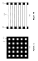
- FIG. 3 shows an embodiment of the micro-integrator rod array of the present invention.
- FIG. 3A shows the front view the micro-integrator rod array 11 ;
- FIG. 3B shows the side view of the micro-integrator rod array 11 .
- FIG. 4 shows an embodiment of the micro-scanning slit array of the present invention.
- FIG. 5 shows another embodiment of the micro-scanning slit array of the present invention.
- FIG. 6 shows a homogenization schematic diagram of the integral rod of the prior art.
- FIG. 7 shows a simple schematic diagram of the homogenization and scanning image of the lithography illumination system of the present invention.
- the lithography illumination system of the present invention comprises a laser light source 1 , a collimating and expanding unit 2 , a pupil shaping unit 3 , a first micro-lens array 4 , a second micro-lens array 5 , a condenser lens group 6 , a micro-scanning slit array 7 , a mask 9 , a motion control unit 10 , and a micro-integrator rod array 11 .
- the components are spatially arranged as follows: a beam emitted from the laser light source 1 sequentially passes through the collimating and expanding unit 2 , the pupil shaping unit 3 , the first micro-lens array 4 , the micro-integrator rod array 11 , the micro-scanning slit array 7 , the second micro-lens array 5 , and the condenser lens group 6 , and then, illuminates the mask 9 ; the motion control unit 10 is connected to the micro-scanning slit array 7 for controlling the moving speed and distance of the micro-scanning slit array 7 to scan the light field; the first micro-lens array 4 is located at the exit pupil plane of the pupil shaping unit 3 ; the entrance end surface of the micro-integrator rod array 11 is located at the back focal plane of the first micro-lens array 4 ; the exit end surface of the micro-integrator rod array 11 is located at the front focal plane of the second micro-lens array 5 ; the back focal plane of the second micro-lens array
- the first micro-lens array 4 is composed of multiple identical first micro-lenses 41 ; the first micro-lenses 41 are closely linked to each other; and the first micro-lens 41 is a cylindrical lens or spherical lens.
- the second micro-lens array 5 is composed of multiple identical second micro-lenses 51 ; the second micro-lenses 51 are closely linked to each other; the second micro-lens 51 is a cylindrical lens or spherical lens; and the field angle of the second micro-lens 51 is different from that of the first micro-lens 41 .
- the micro-integrator rod array 11 is composed of multiple identical micro-integrator rods 111 ; the micro-integrator rod 111 is rectangular; the micro-integrator rod 111 , the first micro-lens 41 and the second micro-lens 51 are in one-to-one correspondence.
- the two ends of the micro-integrator rods 111 are respectively fixed by the first support frame 112 and the second support frame 113 in a two-dimension matrix with an interval, the size of the interval is equal to or greater than that of the end surface of the micro-integrator rod 111 .
- the micro-scanning slit array 7 is composed of multiple identical micro-scanning slits 71 ; the micro-scanning slit 71 is located at the exit end surface of the micro-integrator rod 111 and interspersed in the intervals of the micro-integrator rods 111 .
- the black part indicates opaque portion
- the white part indicates nonopaque portion which is the micro-scanning slit 71 .
- a two micro-scanning slit array is adopted with different nonopaque directions to superposition.
- the motion control unit 10 When the second micro-scanning slit array whose nonopaque direction is along X axis is controlled by the motion control unit 10 to move along Y axis, the Y-direction of the light field is scanned. So when two micro-scanning slit arrays respectively and simultaneously move along X axis and Y axis, the light field is scanned in two dimension.
- the two micro-scanning slit arrays shown in FIG. 4 are combined and integrated into one micro-scanning slit array.
- the motion control unit 10 When it is controlled by the motion control unit 10 to move along X axis, the X-direction of the light field is scanned, when moving along Y axis, the Y-direction of the light field is scanned, and when moving along the angle bisectors of the X axis and Y axis, the light field is scanned in two dimension.
- the motion control unit 10 is to control the micro-scanning slit array 7 to move in one dimension or two dimension.
- Each of them has a corresponding image point on the image plane of Lens 2 (such as P 0 , P 1 etc. shown in FIG. 6 ), and then, the corresponding thin beam is imaged onto the same area of the image plane of Lens 2 . So the superposition of these thin beams generates a uniform light field on the image plane of Lens 2 .
- FIG. 7 the simple schematic diagram of the homogenization and scanning image of the lithography illumination system of the present invention is illustrated.
- the beam is segmented and coupled into the micro-integrator rod array 11 by the first micro-lens array 4 after passing through the pupil shaping unit 3 . Every segmented sub-beam is repeatedly reflected and turned in the corresponding micro-integrator rod 111 , and then form a uniform light field at the exit end surface of the micro-integrator rod 111 .
- the exit end surfaces of the micro-integrator rods 111 are equivalent to the same sub-light sources.
- These sub-light sources are respectively located in the front focal planes of the second micro-lenses 51 , so that the beam is changed into parallel light after passing through the micro-lens 51 and then is focused and imaged onto the mask 9 by the condenser lens group 6 .
- the beam emitted from the same positions of the exit end surfaces of the micro-integrator rods 111 is focused on the same point of the mask 9 after passing through the second micro-lens 51 and the condenser lens group 6 .
- the light field on the mask 9 is the superposition of the uniform light field on the exit end surface of each micro-integrator rod 111 , so that a uniform light field is formed on the mask 9 .
- the micro-scanning slit 71 scans the uniform light field on the exit end surface of the micro-integrator rod 111 , the light field on the mask 9 is accordingly be scanned.
- the homogenizer is skillfully combined with the scanning slit, which eliminates the use of illumination lens group.
- the light field exit from the micro-integrator rod array 11 is non-polarized because of the repeated reflection of the micro-integrator rod 111 so that achieving non-polarized illumination. It should be noted that when the size of the end surface of the micro-integrator rod 111 is fixed, the longer the micro-integrator rod 111 is, the better its homogenization effect is, but the greater absorption loss is. So the requirement of the system transmittance must be considered while pursuing highly uniform light field.
- the lithography illumination system of the present invention adopts a micro-integrator rod array and a micro-scanning slit array to achieve homogenization and scanning.
- the system greatly decreases the scanning distance and scanning speed of the scanning slit to reduce the vibration impact, eliminates the use of illumination lens group to greatly improve system's transmittance, simplifies the system's structure, and achieves non-polarized illumination.
Landscapes
- Physics & Mathematics (AREA)
- General Physics & Mathematics (AREA)
- Optics & Photonics (AREA)
- Exposure And Positioning Against Photoresist Photosensitive Materials (AREA)
- Exposure Of Semiconductors, Excluding Electron Or Ion Beam Exposure (AREA)
Applications Claiming Priority (4)
| Application Number | Priority Date | Filing Date | Title |
|---|---|---|---|
| CN201310030574 | 2013-01-25 | ||
| CN201310030574.9A CN103092006B (zh) | 2013-01-25 | 2013-01-25 | 光刻照明系统 |
| CN201310030574.9 | 2013-01-25 | ||
| PCT/CN2013/000493 WO2014113905A1 (fr) | 2013-01-25 | 2013-04-28 | Système d'éclairement pour lithographie |
Related Parent Applications (1)
| Application Number | Title | Priority Date | Filing Date |
|---|---|---|---|
| PCT/CN2013/000493 Continuation-In-Part WO2014113905A1 (fr) | 2013-01-25 | 2013-04-28 | Système d'éclairement pour lithographie |
Publications (2)
| Publication Number | Publication Date |
|---|---|
| US20150286144A1 US20150286144A1 (en) | 2015-10-08 |
| US9400433B2 true US9400433B2 (en) | 2016-07-26 |
Family
ID=48204748
Family Applications (1)
| Application Number | Title | Priority Date | Filing Date |
|---|---|---|---|
| US14/745,361 Expired - Fee Related US9400433B2 (en) | 2013-01-25 | 2015-06-19 | Lithography illumination system |
Country Status (4)
| Country | Link |
|---|---|
| US (1) | US9400433B2 (fr) |
| EP (1) | EP2950145B1 (fr) |
| CN (1) | CN103092006B (fr) |
| WO (1) | WO2014113905A1 (fr) |
Families Citing this family (16)
| Publication number | Priority date | Publication date | Assignee | Title |
|---|---|---|---|---|
| CN103309175B (zh) * | 2013-06-07 | 2015-06-17 | 中国科学院上海光学精密机械研究所 | 光刻机照明系统的级联微透镜阵列的对准装置和对准方法 |
| CN103412465B (zh) | 2013-07-01 | 2015-04-15 | 中国科学院上海光学精密机械研究所 | 步进扫描投影光刻机的照明系统 |
| CN103399463B (zh) * | 2013-07-19 | 2015-07-29 | 中国科学院上海光学精密机械研究所 | 投影光刻机照明装置和使用方法 |
| CN105805609B (zh) * | 2014-12-31 | 2019-03-12 | 上海微电子装备(集团)股份有限公司 | 一种led光源照明系统 |
| CN104865801B (zh) * | 2015-06-01 | 2017-03-01 | 京东方科技集团股份有限公司 | 曝光装置 |
| JP6540331B2 (ja) * | 2015-07-29 | 2019-07-10 | シーシーエス株式会社 | ライン光照射装置 |
| CN105093848B (zh) * | 2015-08-06 | 2018-01-16 | 武汉华星光电技术有限公司 | 一种曝光设备 |
| CN105589300A (zh) * | 2016-01-07 | 2016-05-18 | 中国科学院上海光学精密机械研究所 | 一种光刻照明系统 |
| CN105842847B (zh) * | 2016-06-02 | 2018-08-31 | 湖北三江航天万峰科技发展有限公司 | 一种利用微透镜阵列进行扫描的激光成像光学系统 |
| US10451890B2 (en) | 2017-01-16 | 2019-10-22 | Cymer, Llc | Reducing speckle in an excimer light source |
| CN110967930B (zh) * | 2018-09-30 | 2021-06-11 | 上海微电子装备(集团)股份有限公司 | 光源衰减装置及光刻机 |
| CN111650745B (zh) * | 2020-07-24 | 2022-07-19 | 中国科学院光电技术研究所 | 一种基于微透镜阵列组和自适应光纤准直器的扫描系统 |
| CN114675494A (zh) * | 2020-12-24 | 2022-06-28 | 中国科学院微电子研究所 | 光刻机照明系统及光刻机 |
| CN115542679B (zh) * | 2022-09-05 | 2024-04-26 | 上海镭望光学科技有限公司 | 调制板透过率分布生成方法、调制板及光刻机照明系统 |
| WO2025210084A1 (fr) * | 2024-04-05 | 2025-10-09 | Iccs (Research University Institute) | Dispositif d'imagerie multicanal, appareil d'imagerie multicanal mettant en œuvre un tel dispositif d'imagerie multicanal ainsi qu'un procédé mis en œuvre par ordinateur pour traiter des données d'image obtenues avec un tel dispositif d'imagerie multicanal |
| NL2037451B1 (en) * | 2024-04-05 | 2025-10-28 | Iccs Research Univ Institute | A multichannel imaging device, a multichannel imaging apparatus implementing such multichannel imaging device as well as a computer implemented method for processing image data obtained with such multichannel imaging device. |
Citations (9)
| Publication number | Priority date | Publication date | Assignee | Title |
|---|---|---|---|---|
| US20020109108A1 (en) | 2001-01-15 | 2002-08-15 | Satoru Mizouchi | Illumination apparatus and projection exposure apparatus using the same |
| US7187430B2 (en) | 2002-06-11 | 2007-03-06 | Asml Holding N.V. | Advanced illumination system for use in microlithography |
| US20070146853A1 (en) | 2005-11-10 | 2007-06-28 | Carl Zeiss Smt Ag | Optical device with raster elements, and illumination system with the optical device |
| US20070165202A1 (en) * | 2003-09-12 | 2007-07-19 | Carl Zeiss Smt Ag | Illumination system for a microlithography projection exposure installation |
| CN101174093A (zh) | 2006-11-03 | 2008-05-07 | 上海微电子装备有限公司 | 一种光刻照明系统 |
| CN101916047A (zh) | 2010-07-27 | 2010-12-15 | 浙江大学 | 一种采用自由曲面透镜实现离轴照明的光刻曝光装置 |
| CN102566294A (zh) | 2010-12-28 | 2012-07-11 | 上海微电子装备有限公司 | 一种光刻照明光学系统 |
| US9110383B2 (en) * | 2005-03-15 | 2015-08-18 | Carl Zeiss Smt Gmbh | Projection exposure method and projection exposure system therefor |
| US20160109808A1 (en) * | 2013-07-01 | 2016-04-21 | Shanghai Institute Of Optics And Fine Mechanics, Chinese Academy Of Sciences | Illumination system for lithographic projection exposure step-and-scan apparatus |
Family Cites Families (8)
| Publication number | Priority date | Publication date | Assignee | Title |
|---|---|---|---|---|
| US7656504B1 (en) * | 1990-08-21 | 2010-02-02 | Nikon Corporation | Projection exposure apparatus with luminous flux distribution |
| CN1717777A (zh) * | 2002-12-03 | 2006-01-04 | 株式会社尼康 | 光学照明装置、曝光装置以及曝光方法 |
| US7187399B2 (en) * | 2003-07-31 | 2007-03-06 | Fuji Photo Film Co., Ltd. | Exposure head with spatial light modulator |
| JP4864869B2 (ja) * | 2004-02-26 | 2012-02-01 | カール・ツァイス・エスエムティー・ゲーエムベーハー | マイクロリソグラフィ投影露光装置のための照明系 |
| CN101587302B (zh) * | 2006-11-03 | 2011-10-12 | 上海微电子装备有限公司 | 一种光刻照明系统 |
| EP2253997A3 (fr) * | 2009-05-18 | 2010-12-08 | Süss MicroTec Lithography GmbH | Système d'éclairage pour contact micro-lithographique et appareil d'exposition de proximité |
| JP2011216863A (ja) * | 2010-03-17 | 2011-10-27 | Hitachi Via Mechanics Ltd | ビームサイズ可変照明光学装置及びビームサイズ変更方法 |
| CN102053372B (zh) * | 2011-01-27 | 2012-05-30 | 清华大学 | 一种改进的光束匀化装置的研制 |
-
2013
- 2013-01-25 CN CN201310030574.9A patent/CN103092006B/zh not_active Expired - Fee Related
- 2013-04-28 WO PCT/CN2013/000493 patent/WO2014113905A1/fr not_active Ceased
- 2013-04-28 EP EP13872643.5A patent/EP2950145B1/fr not_active Not-in-force
-
2015
- 2015-06-19 US US14/745,361 patent/US9400433B2/en not_active Expired - Fee Related
Patent Citations (9)
| Publication number | Priority date | Publication date | Assignee | Title |
|---|---|---|---|---|
| US20020109108A1 (en) | 2001-01-15 | 2002-08-15 | Satoru Mizouchi | Illumination apparatus and projection exposure apparatus using the same |
| US7187430B2 (en) | 2002-06-11 | 2007-03-06 | Asml Holding N.V. | Advanced illumination system for use in microlithography |
| US20070165202A1 (en) * | 2003-09-12 | 2007-07-19 | Carl Zeiss Smt Ag | Illumination system for a microlithography projection exposure installation |
| US9110383B2 (en) * | 2005-03-15 | 2015-08-18 | Carl Zeiss Smt Gmbh | Projection exposure method and projection exposure system therefor |
| US20070146853A1 (en) | 2005-11-10 | 2007-06-28 | Carl Zeiss Smt Ag | Optical device with raster elements, and illumination system with the optical device |
| CN101174093A (zh) | 2006-11-03 | 2008-05-07 | 上海微电子装备有限公司 | 一种光刻照明系统 |
| CN101916047A (zh) | 2010-07-27 | 2010-12-15 | 浙江大学 | 一种采用自由曲面透镜实现离轴照明的光刻曝光装置 |
| CN102566294A (zh) | 2010-12-28 | 2012-07-11 | 上海微电子装备有限公司 | 一种光刻照明光学系统 |
| US20160109808A1 (en) * | 2013-07-01 | 2016-04-21 | Shanghai Institute Of Optics And Fine Mechanics, Chinese Academy Of Sciences | Illumination system for lithographic projection exposure step-and-scan apparatus |
Non-Patent Citations (3)
| Title |
|---|
| Han, Jingfu, "Optical parts in the MD projector (IV)-micro lens array and rod integrator," Advanced Display, No. 111, pp. 5-7 and 12 (Apr. 2010) ISSN 1006-6268. |
| Jorg Zimmermann et al., "Generation of arbitrary freeform source shapes using advanced illumination systems in high-NA immersion scanners," Proc. of SPIE, vol. 7640, p. 764005 (2010). |
| Liping Guo et al., "Study of integrator rod in step-and-scan lithography," Acta Photonica Sinica, vol. 35(7), pp. 981-985 (2006) ISSN 1004-4213. |
Also Published As
| Publication number | Publication date |
|---|---|
| US20150286144A1 (en) | 2015-10-08 |
| WO2014113905A1 (fr) | 2014-07-31 |
| CN103092006B (zh) | 2015-02-18 |
| EP2950145A4 (fr) | 2017-01-25 |
| CN103092006A (zh) | 2013-05-08 |
| EP2950145A1 (fr) | 2015-12-02 |
| EP2950145B1 (fr) | 2017-09-20 |
Similar Documents
| Publication | Publication Date | Title |
|---|---|---|
| US9400433B2 (en) | Lithography illumination system | |
| US20080084612A1 (en) | Apparatus for generating a homogeneous angular distribution of laser irradiation | |
| CN101936504B (zh) | 一种用于光刻多极照明的自由曲面微透镜阵列装置 | |
| JP6270166B2 (ja) | リソグラフィ投影露光装置の照明視野にわたる照明強度を予め定めるための照明強度補正デバイス | |
| US9766442B2 (en) | Confocal scanner and confocal microscope | |
| KR102397041B1 (ko) | 조명 광학계, 노광 방법 및 디바이스 제조 방법 | |
| KR102853114B1 (ko) | 투영 노광 장치용 광학 시스템 | |
| JP2002514007A (ja) | 特にeuv(極紫外線)リソグラフィーに用いる照射機構 | |
| KR20050041985A (ko) | 광학적 광선변환을 위한 배열 및 장치 | |
| CN104364715B (zh) | 用于投射光刻的照明光学单元 | |
| JP2006523944A (ja) | 照明装置のための光学素子 | |
| CN110456612A (zh) | 一种高效率投影光刻成像系统及曝光方法 | |
| JP6614882B2 (ja) | レーザラインジェネレータのための導光体ベースの光学システム | |
| CN109031899A (zh) | 一种高分辨率高效率投影光刻成像系统及曝光方法 | |
| CN103412465B (zh) | 步进扫描投影光刻机的照明系统 | |
| CN100559277C (zh) | 一种光刻照明系统 | |
| KR20110120872A (ko) | 레이저 노광 장치 | |
| KR102344281B1 (ko) | 콜렉터 | |
| KR20070057074A (ko) | 광 균일화 장치 및 상기 광 균일화 장치를 구비한 조명장치 또는 포커싱 장치 | |
| CN104460242A (zh) | 一种基于自由曲面式光阑复眼的极紫外光刻照明系统 | |
| KR101388406B1 (ko) | Euv 투영 리소그래피용 조명 광학 유닛에 대한 조명 기하구조 설정 방법 | |
| TW200419203A (en) | Exposure apparatus | |
| CN110133843A (zh) | 一种激光扫描单元以及激光打印机 | |
| CN103309175B (zh) | 光刻机照明系统的级联微透镜阵列的对准装置和对准方法 | |
| CN108693688B (zh) | 光源系统及投影设备 |
Legal Events
| Date | Code | Title | Description |
|---|---|---|---|
| AS | Assignment |
Owner name: SHANGHAI INSTITUTE OF OPTICS AND FINE MECHANICS, C Free format text: ASSIGNMENT OF ASSIGNORS INTEREST;ASSIGNORS:ZENG, AIJUN;ZHU, LINGLIN;FANG, RUIFANG;AND OTHERS;REEL/FRAME:035873/0027 Effective date: 20150615 |
|
| STCF | Information on status: patent grant |
Free format text: PATENTED CASE |
|
| MAFP | Maintenance fee payment |
Free format text: PAYMENT OF MAINTENANCE FEE, 4TH YR, SMALL ENTITY (ORIGINAL EVENT CODE: M2551); ENTITY STATUS OF PATENT OWNER: SMALL ENTITY Year of fee payment: 4 |
|
| FEPP | Fee payment procedure |
Free format text: MAINTENANCE FEE REMINDER MAILED (ORIGINAL EVENT CODE: REM.); ENTITY STATUS OF PATENT OWNER: SMALL ENTITY |
|
| LAPS | Lapse for failure to pay maintenance fees |
Free format text: PATENT EXPIRED FOR FAILURE TO PAY MAINTENANCE FEES (ORIGINAL EVENT CODE: EXP.); ENTITY STATUS OF PATENT OWNER: SMALL ENTITY |
|
| STCH | Information on status: patent discontinuation |
Free format text: PATENT EXPIRED DUE TO NONPAYMENT OF MAINTENANCE FEES UNDER 37 CFR 1.362 |
|
| FP | Lapsed due to failure to pay maintenance fee |
Effective date: 20240726 |