US9431592B2 - Submount with cavities and through vias for LED packaging - Google Patents
Submount with cavities and through vias for LED packaging Download PDFInfo
- Publication number
- US9431592B2 US9431592B2 US14/122,929 US201214122929A US9431592B2 US 9431592 B2 US9431592 B2 US 9431592B2 US 201214122929 A US201214122929 A US 201214122929A US 9431592 B2 US9431592 B2 US 9431592B2
- Authority
- US
- United States
- Prior art keywords
- substrate
- vias
- cavity
- providing
- metal
- Prior art date
- Legal status (The legal status is an assumption and is not a legal conclusion. Google has not performed a legal analysis and makes no representation as to the accuracy of the status listed.)
- Active, expires
Links
Images




Classifications
-
- H—ELECTRICITY
- H10—SEMICONDUCTOR DEVICES; ELECTRIC SOLID-STATE DEVICES NOT OTHERWISE PROVIDED FOR
- H10H—INORGANIC LIGHT-EMITTING SEMICONDUCTOR DEVICES HAVING POTENTIAL BARRIERS
- H10H20/00—Individual inorganic light-emitting semiconductor devices having potential barriers, e.g. light-emitting diodes [LED]
- H10H20/80—Constructional details
- H10H20/85—Packages
- H10H20/857—Interconnections, e.g. lead-frames, bond wires or solder balls
-
- H01L33/62—
-
- H01L24/16—
-
- H01L25/075—
-
- H—ELECTRICITY
- H10—SEMICONDUCTOR DEVICES; ELECTRIC SOLID-STATE DEVICES NOT OTHERWISE PROVIDED FOR
- H10W—GENERIC PACKAGES, INTERCONNECTIONS, CONNECTORS OR OTHER CONSTRUCTIONAL DETAILS OF DEVICES COVERED BY CLASS H10
- H10W90/00—Package configurations
-
- H01L2224/16—
-
- H01L2224/16145—
-
- H01L2224/48091—
-
- H01L2224/48247—
-
- H01L2224/48465—
-
- H01L2924/00—
-
- H01L2924/00012—
-
- H01L2924/00014—
-
- H01L2924/01029—
-
- H01L2924/10253—
-
- H01L2924/12041—
-
- H01L2933/0033—
-
- H01L33/502—
-
- H—ELECTRICITY
- H10—SEMICONDUCTOR DEVICES; ELECTRIC SOLID-STATE DEVICES NOT OTHERWISE PROVIDED FOR
- H10H—INORGANIC LIGHT-EMITTING SEMICONDUCTOR DEVICES HAVING POTENTIAL BARRIERS
- H10H20/00—Individual inorganic light-emitting semiconductor devices having potential barriers, e.g. light-emitting diodes [LED]
- H10H20/01—Manufacture or treatment
- H10H20/036—Manufacture or treatment of packages
-
- H—ELECTRICITY
- H10—SEMICONDUCTOR DEVICES; ELECTRIC SOLID-STATE DEVICES NOT OTHERWISE PROVIDED FOR
- H10H—INORGANIC LIGHT-EMITTING SEMICONDUCTOR DEVICES HAVING POTENTIAL BARRIERS
- H10H20/00—Individual inorganic light-emitting semiconductor devices having potential barriers, e.g. light-emitting diodes [LED]
- H10H20/80—Constructional details
- H10H20/85—Packages
- H10H20/851—Wavelength conversion means
- H10H20/8511—Wavelength conversion means characterised by their material, e.g. binder
- H10H20/8512—Wavelength conversion materials
-
- H—ELECTRICITY
- H10—SEMICONDUCTOR DEVICES; ELECTRIC SOLID-STATE DEVICES NOT OTHERWISE PROVIDED FOR
- H10W—GENERIC PACKAGES, INTERCONNECTIONS, CONNECTORS OR OTHER CONSTRUCTIONAL DETAILS OF DEVICES COVERED BY CLASS H10
- H10W72/00—Interconnections or connectors in packages
- H10W72/071—Connecting or disconnecting
- H10W72/072—Connecting or disconnecting of bump connectors
- H10W72/07251—Connecting or disconnecting of bump connectors characterised by changes in properties of the bump connectors during connecting
-
- H—ELECTRICITY
- H10—SEMICONDUCTOR DEVICES; ELECTRIC SOLID-STATE DEVICES NOT OTHERWISE PROVIDED FOR
- H10W—GENERIC PACKAGES, INTERCONNECTIONS, CONNECTORS OR OTHER CONSTRUCTIONAL DETAILS OF DEVICES COVERED BY CLASS H10
- H10W72/00—Interconnections or connectors in packages
- H10W72/20—Bump connectors, e.g. solder bumps or copper pillars; Dummy bumps; Thermal bumps
-
- H—ELECTRICITY
- H10—SEMICONDUCTOR DEVICES; ELECTRIC SOLID-STATE DEVICES NOT OTHERWISE PROVIDED FOR
- H10W—GENERIC PACKAGES, INTERCONNECTIONS, CONNECTORS OR OTHER CONSTRUCTIONAL DETAILS OF DEVICES COVERED BY CLASS H10
- H10W72/00—Interconnections or connectors in packages
- H10W72/50—Bond wires
- H10W72/531—Shapes of wire connectors
- H10W72/536—Shapes of wire connectors the connected ends being ball-shaped
-
- H—ELECTRICITY
- H10—SEMICONDUCTOR DEVICES; ELECTRIC SOLID-STATE DEVICES NOT OTHERWISE PROVIDED FOR
- H10W—GENERIC PACKAGES, INTERCONNECTIONS, CONNECTORS OR OTHER CONSTRUCTIONAL DETAILS OF DEVICES COVERED BY CLASS H10
- H10W72/00—Interconnections or connectors in packages
- H10W72/50—Bond wires
- H10W72/531—Shapes of wire connectors
- H10W72/5363—Shapes of wire connectors the connected ends being wedge-shaped
-
- H—ELECTRICITY
- H10—SEMICONDUCTOR DEVICES; ELECTRIC SOLID-STATE DEVICES NOT OTHERWISE PROVIDED FOR
- H10W—GENERIC PACKAGES, INTERCONNECTIONS, CONNECTORS OR OTHER CONSTRUCTIONAL DETAILS OF DEVICES COVERED BY CLASS H10
- H10W90/00—Package configurations
- H10W90/701—Package configurations characterised by the relative positions of pads or connectors relative to package parts
- H10W90/721—Package configurations characterised by the relative positions of pads or connectors relative to package parts of bump connectors
- H10W90/722—Package configurations characterised by the relative positions of pads or connectors relative to package parts of bump connectors between stacked chips
-
- H—ELECTRICITY
- H10—SEMICONDUCTOR DEVICES; ELECTRIC SOLID-STATE DEVICES NOT OTHERWISE PROVIDED FOR
- H10W—GENERIC PACKAGES, INTERCONNECTIONS, CONNECTORS OR OTHER CONSTRUCTIONAL DETAILS OF DEVICES COVERED BY CLASS H10
- H10W90/00—Package configurations
- H10W90/701—Package configurations characterised by the relative positions of pads or connectors relative to package parts
- H10W90/751—Package configurations characterised by the relative positions of pads or connectors relative to package parts of bond wires
- H10W90/756—Package configurations characterised by the relative positions of pads or connectors relative to package parts of bond wires between a chip and a stacked lead frame, conducting package substrate or heat sink
Definitions
- the present invention relates to light emitting diodes and more specifically to a structure and method for packaging light emitting diodes.
- LEDs Light Emitting Diodes
- pc-LED phosphor-converted LED
- RGB Red, Green, Blue
- UV LEDs with RGB phosphors method ultraviolet LEDs with RGB phosphors
- FIG. 1 is an example of a sectional view of a conventional LED package 100 .
- an LED chip 113 is flip chip bonded by solder joints 115 to a flat silicon submount 117 including metal circuits (not shown) for electric connection between the LED chip 113 and the submount 117 .
- the submount 117 with the LED chip 113 bonded together is then attached to a heat sink 101 by an adhesive 119 .
- the LED package 100 includes leads 107 which are held by a plastic body 105 and are wire bonded 103 to the silicon submount 117 to realize the electric connection.
- a lens (encapsulant) 111 which is fabricated in advance, covers the LED chip 113 , wires 103 and the submount 117 .
- the whole package is finally attached to the board 109 (e.g., a printed circuit board (PCB)) which performs electric signal distribution and heat dissipation.
- PCB printed circuit board
- the process of fabricating the LED package 100 shown in FIG. 1 suffers from high cost due to its complicated structure. Moreover, conventional LED dies are encapsulated individually, precluding the implementation of a mass production process that could potentially provide high yield with low cost.
- the present invention provides a wafer having a plurality of light-emitting diode (LED) submounts.
- Each of the plurality of LED submounts of the wafer includes: a substrate, including through vias; an LED die mounted in a cavity on a first side of the substrate and connected to the through vias; and a redistribution layer attached to a second side of the substrate connected to the LED die through the through vias.
- the present invention provides a method for fabricating a light-emitting diode (LED) submount.
- the method includes providing a wafer as a substrate; providing a cavity in the substrate on a first side of the substrate; providing through vias in the substrate, providing a redistribution layer on the second side of the substrate, and mounting an LED in the cavity, wherein the LED die is connected to the redistribution layer through the through vias.
- Providing the through vias includes providing blind vias in the substrate on a second side of the substrate; filling the blind vias with metal; and etching the substrate such that the metal in the blind vias is exposed in the cavity so as to produce the through vias.
- Providing the redistribution layer includes: providing a metal layer on the second side of the substrate; and patterning the metal layer so as to produce the redistribution layer.
- FIG. 1 is a diagram of an example of a conventional LED package
- FIG. 2 is a diagram illustrating the components of an LED submount in accordance with the described principles
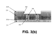
- FIGS. 3( a ) through 3( h ) are diagrams illustrating an LED submount during different stages of the fabrication process in accordance with the described principles
- FIG. 4 is a diagram illustrating an LED submount having a transparent or translucent plate in accordance with the described principles
- FIG. 5 is a diagram illustrating an LED submount having a transparent or translucent plate and a layer of encapsulant mixed with phosphor powder in accordance with the described principles
- FIG. 6 is a diagram illustrating a reflective layer provided within the cavity of an LED submount in accordance with the described principles.
- Embodiments of the present invention contemplate a structure and fabrication process of a substrate with cavities and through vias for LED packaging.
- the process starts with the fabrication of blind holes on the backside and cavities on the front-side of the substrate.
- the substrate can be silicon, PCB, MCPCB, BT, glass, ceramic, plastic, metal, or made of other materials.
- blind hole refers to a small hole that does not go through the entire substrate.
- the blind holes fabricated on the backside of substrate are filled with metal, such as copper, through an electroplating process that also covers the backside of the submount with metal.
- the cavities on the front-side are further etched down to expose the metal, forming “through vias” (also referred to as “through silicon vias” (TSVs)) that connect the top side of the submount to the bottom side of the submount.
- through vias also referred to as “through silicon vias” (TSVs)
- TSVs through silicon vias
- the cavities are where LED dies are mounted (as described in further below with respect to FIG. 3( g ) ).
- the metal layer on the backside of the submount is patterned with a desired circuit.
- the through vias structure generated by this process enables three-dimensional (3D) interconnection from the front-side to the backside of the substrate, which allows for electric interconnections not only on the surface of the submount (i.e., “horizontally”), but also to the bottom side of the submount through the “through vias” (i.e., “vertically”).
- the use of cavities allow for printing or injecting processes to fill the cavity with encapsulant, such that it is unnecessary to use a mold to coat the LED dies.
- Encapsulant with phosphor powders protects the LED dies and converts blue light into white light. It will be appreciated that this process overcomes a problem associated with conventional LED packaging where circuits could not be patterned on the bottom of the cavities of the front-side of the substrate.
- FIG. 2 a schematic diagram is depicted showing a cross-section of a submount 200 according to the LED packaging structure of an embodiment.
- the packaging structure includes a core substrate 201 , insulation layers 202 a and 202 b , through vias 203 a on the backside of the substrate, a cavity 204 on the front-side of the substrate, a redistribution layer 205 a on the backside of the substrate, metal pillars 206 connecting the bottom of the cavities 204 to the backside of the substrate, solder bumps 207 , LED die 208 , and encapsulant 209 , which is a mixture of phosphor powder and encapsulant.
- the submounts depicted in FIGS. 2 through 6 may be part of a wafer including a large number of such submounts—e.g., tens of thousands of such units.
- the processes described below with respect to FIGS. 3( a ) through 3( h ) and FIGS. 4 through 6 may be performed simultaneously on the wafer for a plurality of LED packages. After the processes described below have been completed, the wafer can then be separated into individual packages.
- FIGS. 3( a ) through 3( h ) a cross-section of an LED packaging structure is shown at various stages throughout a process of fabricating the LED packaging structure according to an embodiment of the present invention.
- insulation layers 202 a and 202 b are attached to a core substrate 201 by deposition, diffusion or printing.
- the blind vias 203 and cavity 204 are first fabricated by a process, for example, including but not limited to etching or mechanical milling.
- the insulation layers 202 a and 202 b can serve as etching masks for the top side and the bottom side, respectively.
- the insulation layer 202 a may need to be re-attached or extended to cover the side walls of the blind vias 203 through further deposition, diffusion, or printing.
- metal is filled into the blind vias 203 to form metal pillars 206 .
- the filling can be done with an electroplating process.
- a metal layer 205 covering the backside of the substrate 201 can be provided simultaneously with the metal pillars 206 or later on in the process (e.g., after deepening the cavity 204 as described below with respect to FIG. 3( c ) ).
- the metal layer 205 and the metal pillars 206 may further be provided, for example, by sputtering or evaporation.
- the cavity 204 on the front-side is deepened by a process—for example, including but not limited to, etching or mechanical milling—until the tips of the metal pillars 206 are exposed.
- the blind vias 203 are now referred to as through vias 203 a , which connect the top side of the submount with the bottom side of the submount.
- solder 207 a is plated on the tips of the metal pillars 206 .
- the process can be done by electroplating.
- this electroplating is performed by connecting the metal layer of a wafer to a cathode (depicted as electrodes 221 a and 221 b in FIG. 3( d ) ) and connecting a solder plate to an anode (not pictured), and immersing both in a plating solution such that when an electric current is applied, solder ions are released from the solder plate and dissolve into the plating solution.
- solder 207 a on the tips of the metal pillars 206 .
- the individual metal pillars 206 are connected by a metal layer 205 on the backside, which is covered by an insulation layer 220 to prevent the metal layer 205 from being plated with solder.
- the insulation layer 220 is removed, and the metal layer 205 should remain attached.
- the insulation layer 220 is photoresist that is attached by thermal diffusion or chemical vapor deposition processes and removed by organic solvents. It will be appreciated that the electrodes 221 a and 221 b shown in FIG.
- the electroplating can be performed so long as the electrodes 221 a and 221 b contact any region of the metal layer of the wafer.
- the whole substrate goes through a reflow process, which results in the solder bumps 207 being formed.
- a reflow oven having several heating zones and a conveyor belt is used.
- a wafer including one or more submounts is put on the conveyor belt and goes through different heating zones of the oven.
- the wafer is heated up and then cooled down in the oven under a controlled reflow profile.
- the process causes the solder 207 a to form a spherical shape (solder bumps 207 ) due to the effect of surface tension.
- the metal layer 205 is patterned into a redistribution layer 205 a on the backside, connecting the metal pillars 206 in a desired circuit pattern.
- the patterning is performed using photolithography. Two or more traces are connected to the anode and cathode of each LED die to pass direct current through the device and light up the LED after the LED has been mounted.
- an LED die 208 is mounted in the cavity 204 on the solder bumps 207 .
- the mounting is performed with a reflow oven using conventional flip-chip mounting techniques.
- a single cavity 204 can contain more than one LED die, depending on the design.
- the cavity 204 contains three LED dies, including red, green, and blue LED dies, all mounted within the same cavity.
- the cavity contains four LED dies, including one red, one blue, and two green dies. The power supplied to each of the individual LEDs dies is controlled through the circuit connected to the LEDs.
- encapsulant 209 is filled into the cavity 204 , for example, by needle dispensing or screen printing.
- the encapsulant 209 is solidified through curing and serves to protect the LED die 208 .
- the material used for the encapsulant 209 can be, for example, silicone or epoxy, and the encapsulant 209 can be transparent or translucent or be mixed with phosphor powders in order to convert the color of the LED light (e.g., from blue light to white light).
- the encapsulant 209 fills the cavity 204 and provides a flat surface level with the front-side of the LED packaging structure. It will be appreciated that in other embodiments, the encapsulant 209 can have other shapes, such as a dome-shape that exceeds the size of the cavity 204 .
- FIG. 4 depicts a further embodiment of the present invention.
- the fabrication process of the substrate is similar to the process described above with respect to FIG. 3( a ) to FIG. 3( h ) , and, additionally, a transparent or translucent plate 210 is provided to cover the front-side of the substrate.
- the plate 210 is added by wafer bonding. Phosphor layers can then be sprayed onto the plate 210 (as shown below in FIG. 5 ) so that the phosphor layers do not directly contact the LED (this configuration is often referred to as “remote phosphor”). This configuration helps prevent the phosphor from being heated up so as to improve the performance of the LED.
- FIG. 5 shows yet another further embodiment of the present invention.
- the fabrication process of the substrate is similar to the process described above with respect to FIG. 3( a ) to FIG. 3( h ) and FIG. 4 , and, additionally, encapsulant 209 mixed with phosphor powder is attached to the plate 210 as shown.
- the cavity 204 can be filled with another type of encapsulant 211 or be left unfilled.
- the same type of encapsulant 209 can be used both for attachment to the plate 210 and to fill the cavity 204 .
- FIG. 6 shows yet another further embodiment of the present invention, where, during the manufacturing process, a reflective layer 230 is attached to the cavity 204 through printing, deposition, or diffusion to increase the reflection of light emitted from the LED dies 208 , as shown in FIG. 6 .
- the layer is produced by sputtering or an evaporation process.
- embodiments of the present invention provide a structure and process that allow for wafer-level packaging (WLP) of LEDs, for example, using a silicon wafer as a substrate.
- WLP provides the advantages of batch fabrication and component integration, which can be achieved using the “through via” structure for three-dimensional interconnections and high thermal conduction.
- embodiments of the present invention provide a cavity structure for optical reflection and allows for mold-free phosphor printing and encapsulation process.
Landscapes
- Led Device Packages (AREA)
Priority Applications (1)
| Application Number | Priority Date | Filing Date | Title |
|---|---|---|---|
| US14/122,929 US9431592B2 (en) | 2011-06-01 | 2012-06-01 | Submount with cavities and through vias for LED packaging |
Applications Claiming Priority (3)
| Application Number | Priority Date | Filing Date | Title |
|---|---|---|---|
| US201161457774P | 2011-06-01 | 2011-06-01 | |
| US14/122,929 US9431592B2 (en) | 2011-06-01 | 2012-06-01 | Submount with cavities and through vias for LED packaging |
| PCT/CN2012/000752 WO2012163086A1 (fr) | 2011-06-01 | 2012-06-01 | Embase à cavités et trous traversants pour le conditionnement de del |
Publications (2)
| Publication Number | Publication Date |
|---|---|
| US20140110728A1 US20140110728A1 (en) | 2014-04-24 |
| US9431592B2 true US9431592B2 (en) | 2016-08-30 |
Family
ID=47258346
Family Applications (1)
| Application Number | Title | Priority Date | Filing Date |
|---|---|---|---|
| US14/122,929 Active 2032-08-17 US9431592B2 (en) | 2011-06-01 | 2012-06-01 | Submount with cavities and through vias for LED packaging |
Country Status (3)
| Country | Link |
|---|---|
| US (1) | US9431592B2 (fr) |
| CN (1) | CN103748700B (fr) |
| WO (1) | WO2012163086A1 (fr) |
Families Citing this family (24)
| Publication number | Priority date | Publication date | Assignee | Title |
|---|---|---|---|---|
| US9502612B2 (en) * | 2009-09-20 | 2016-11-22 | Viagan Ltd. | Light emitting diode package with enhanced heat conduction |
| US9620436B2 (en) | 2014-04-09 | 2017-04-11 | Invensas Corporation | Light emitting diode device with reconstituted LED components on substrate |
| JP2016081959A (ja) * | 2014-10-10 | 2016-05-16 | シチズン電子株式会社 | 発光装置及びその製造方法 |
| CN104638091B (zh) * | 2014-12-18 | 2017-10-24 | 上海大学 | Led玻璃基板 |
| CN104600039B (zh) * | 2014-12-26 | 2018-01-16 | 通富微电子股份有限公司 | 双面互联扇出工艺 |
| CN104659178A (zh) * | 2015-03-09 | 2015-05-27 | 武汉大学 | 一种功率型三维led发光器件及其制造方法 |
| CN104701437A (zh) * | 2015-03-09 | 2015-06-10 | 武汉大学 | 一种三维led发光器件 |
| US9847230B2 (en) * | 2015-06-09 | 2017-12-19 | The Charles Stark Draper Laboratory, Inc. | Method and apparatus for using universal cavity wafer in wafer level packaging |
| JP6711568B2 (ja) * | 2015-07-29 | 2020-06-17 | ローム株式会社 | 半導体装置 |
| US10483253B1 (en) | 2015-09-24 | 2019-11-19 | Apple Inc. | Display with embedded pixel driver chips |
| US10665578B2 (en) | 2015-09-24 | 2020-05-26 | Apple Inc. | Display with embedded pixel driver chips |
| CN105575956B (zh) * | 2015-12-31 | 2017-11-17 | 中国科学院半导体研究所 | Led芯片集成封装模块和封装方法 |
| JP2017175000A (ja) * | 2016-03-24 | 2017-09-28 | ローム株式会社 | 電子部品およびその製造方法、ならびに、インターポーザ |
| JP6748501B2 (ja) * | 2016-07-14 | 2020-09-02 | ローム株式会社 | 電子部品およびその製造方法 |
| KR102701803B1 (ko) * | 2018-06-11 | 2024-09-03 | 서울반도체 주식회사 | 발광 다이오드 패키지 |
| WO2020037677A1 (fr) * | 2018-08-24 | 2020-02-27 | 深圳市汇顶科技股份有限公司 | Procédé et structure d'encapsulayion pour dispositif d'émission de lumière, et dispositif électronique |
| DE102018122166A1 (de) * | 2018-09-11 | 2020-03-12 | Osram Opto Semiconductors Gmbh | Optoelektronische halbleitervorrichtung mit einem trägerelement und einem elektrischen kontaktelement, optoelektronisches bauelement sowie verfahren zur herstellung der optoelektronischen halbleitervorrichtung |
| US10957832B2 (en) * | 2018-10-22 | 2021-03-23 | General Electric Company | Electronics package for light emitting semiconductor devices and method of manufacturing thereof |
| CN109786540B (zh) * | 2019-01-24 | 2021-07-23 | 南通沃特光电科技有限公司 | 一种led封装结构及其封装方法 |
| CN109683396A (zh) * | 2019-01-30 | 2019-04-26 | 厦门天马微电子有限公司 | 背光模组、显示面板、显示装置及背光模组的制作方法 |
| KR102762976B1 (ko) * | 2020-01-03 | 2025-02-07 | 삼성전자주식회사 | 반도체 패키지 |
| CN111883494B (zh) * | 2020-07-21 | 2022-11-29 | 联合微电子中心有限责任公司 | 功率mosfet器件及其形成方法 |
| CN119212738A (zh) * | 2022-03-16 | 2024-12-27 | 优卫魁公司 | 被配置用于在远uvc光谱中的波长下操作的微led |
| US20240063094A1 (en) * | 2022-08-19 | 2024-02-22 | Micron Technology, Inc. | Semiconductor device assemblies with a cavity exposing through-silicon vias for controller attachment |
Citations (15)
| Publication number | Priority date | Publication date | Assignee | Title |
|---|---|---|---|---|
| US20030071366A1 (en) * | 2001-08-21 | 2003-04-17 | General Electric Company | Epoxy resin compositions, solid state devices encapsulated therewith and method |
| US20050274959A1 (en) | 2004-06-10 | 2005-12-15 | Geun-Ho Kim | High power LED package |
| US20070189007A1 (en) | 2004-03-26 | 2007-08-16 | Keiji Nishimoto | Led mounting module, led module, manufacturing method of led mounting module, and manufacturing method of led module |
| US20070215896A1 (en) | 2006-03-17 | 2007-09-20 | Edison Opto Corporation | Light emitting diode package structure and method of manufacturing the same |
| US20070228387A1 (en) | 2006-04-04 | 2007-10-04 | Gerald Negley | Uniform emission LED package |
| US20080179618A1 (en) | 2007-01-26 | 2008-07-31 | Ching-Tai Cheng | Ceramic led package |
| US20090081867A1 (en) | 2007-09-21 | 2009-03-26 | Shinko Electric Industries Co., Ltd. | Method of manufacturing substrate |
| US20090121252A1 (en) * | 2007-11-14 | 2009-05-14 | Hung-Tsung Hsu | Method for manufacturing flip-chip light emitting diode package |
| US7683470B2 (en) | 2006-02-22 | 2010-03-23 | Samsung Electro-Mechanics Co., Ltd. | LED package |
| US20100129960A1 (en) * | 2007-04-27 | 2010-05-27 | Sumitomo Bakelite Company Limited | Method for bonding semiconductor wafers and method for manufacturing semiconductor device |
| US7745832B2 (en) * | 2004-09-24 | 2010-06-29 | Epistar Corporation | Semiconductor light-emitting element assembly with a composite substrate |
| US20100252934A1 (en) * | 2009-04-07 | 2010-10-07 | Taiwan Semiconductor Manufacturing Company, Ltd. | Three-Dimensional Semiconductor Architecture |
| CN201804913U (zh) | 2010-09-30 | 2011-04-20 | 江阴长电先进封装有限公司 | 圆片级led封装结构 |
| US8093711B2 (en) * | 2009-02-02 | 2012-01-10 | Infineon Technologies Ag | Semiconductor device |
| US20130161824A1 (en) * | 2011-12-21 | 2013-06-27 | Stats Chippac, Ltd. | Semiconductor Device and Method of Forming Insulating Layer in Notches Around Conductive TSV for Stress Relief |
-
2012
- 2012-06-01 WO PCT/CN2012/000752 patent/WO2012163086A1/fr not_active Ceased
- 2012-06-01 CN CN201280025715.1A patent/CN103748700B/zh active Active
- 2012-06-01 US US14/122,929 patent/US9431592B2/en active Active
Patent Citations (15)
| Publication number | Priority date | Publication date | Assignee | Title |
|---|---|---|---|---|
| US20030071366A1 (en) * | 2001-08-21 | 2003-04-17 | General Electric Company | Epoxy resin compositions, solid state devices encapsulated therewith and method |
| US20070189007A1 (en) | 2004-03-26 | 2007-08-16 | Keiji Nishimoto | Led mounting module, led module, manufacturing method of led mounting module, and manufacturing method of led module |
| US20050274959A1 (en) | 2004-06-10 | 2005-12-15 | Geun-Ho Kim | High power LED package |
| US7745832B2 (en) * | 2004-09-24 | 2010-06-29 | Epistar Corporation | Semiconductor light-emitting element assembly with a composite substrate |
| US7683470B2 (en) | 2006-02-22 | 2010-03-23 | Samsung Electro-Mechanics Co., Ltd. | LED package |
| US20070215896A1 (en) | 2006-03-17 | 2007-09-20 | Edison Opto Corporation | Light emitting diode package structure and method of manufacturing the same |
| US20070228387A1 (en) | 2006-04-04 | 2007-10-04 | Gerald Negley | Uniform emission LED package |
| US20080179618A1 (en) | 2007-01-26 | 2008-07-31 | Ching-Tai Cheng | Ceramic led package |
| US20100129960A1 (en) * | 2007-04-27 | 2010-05-27 | Sumitomo Bakelite Company Limited | Method for bonding semiconductor wafers and method for manufacturing semiconductor device |
| US20090081867A1 (en) | 2007-09-21 | 2009-03-26 | Shinko Electric Industries Co., Ltd. | Method of manufacturing substrate |
| US20090121252A1 (en) * | 2007-11-14 | 2009-05-14 | Hung-Tsung Hsu | Method for manufacturing flip-chip light emitting diode package |
| US8093711B2 (en) * | 2009-02-02 | 2012-01-10 | Infineon Technologies Ag | Semiconductor device |
| US20100252934A1 (en) * | 2009-04-07 | 2010-10-07 | Taiwan Semiconductor Manufacturing Company, Ltd. | Three-Dimensional Semiconductor Architecture |
| CN201804913U (zh) | 2010-09-30 | 2011-04-20 | 江阴长电先进封装有限公司 | 圆片级led封装结构 |
| US20130161824A1 (en) * | 2011-12-21 | 2013-06-27 | Stats Chippac, Ltd. | Semiconductor Device and Method of Forming Insulating Layer in Notches Around Conductive TSV for Stress Relief |
Non-Patent Citations (3)
| Title |
|---|
| International Search Report and Written Opinion from the International Searching Authority in International Patent Publication No. PCT/CN2012/000752, Sep. 6, 2012. |
| Lim et al., "LED packaging using high sad rectangular microlens array," Micro-Optics, VCSELs, and Photonic Interconnects II: Fabrication, Packaging, and Integration, Process of SPIE, vol. 6185, pp. 6181516-1-7, 2006. |
| Tsou et al., "Silicon-based packaging platform for light-emitting diode," IEEE Transactions on Advanced Packaging, vol. 29(3), pp. 607-614, 2006. |
Also Published As
| Publication number | Publication date |
|---|---|
| CN103748700A (zh) | 2014-04-23 |
| US20140110728A1 (en) | 2014-04-24 |
| CN103748700B (zh) | 2016-11-16 |
| WO2012163086A1 (fr) | 2012-12-06 |
Similar Documents
| Publication | Publication Date | Title |
|---|---|---|
| US9431592B2 (en) | Submount with cavities and through vias for LED packaging | |
| TWI390772B (zh) | 半導體裝置及其製造方法 | |
| US7847302B2 (en) | Blue LED with phosphor layer for producing white light and different phosphor in outer lens for reducing color temperature | |
| US9347646B2 (en) | Light emitting device providing controlled color rendition | |
| TWI476946B (zh) | 發光二極體裝置及其製造方法 | |
| US8952404B2 (en) | Light-emitting device package and method of manufacturing the light-emitting device package | |
| US20110176301A1 (en) | Method to produce homogeneous light output by shaping the light conversion material in multichip module | |
| US20080079017A1 (en) | Method of uniform phosphor chip coating and led package fabricated using method | |
| US20100112735A1 (en) | Chip coated light emitting diode package and manufacturing method thereof | |
| US20120193662A1 (en) | Reflective mounting substrates for flip-chip mounted horizontal leds | |
| US9214607B1 (en) | Wire bonded light emitting diode (LED) components including reflective layer | |
| US20200043905A1 (en) | Light emitting diode (led) components and methods | |
| CN102263194A (zh) | 半导体封装与制造半导体封装的方法 | |
| JP2017108111A (ja) | 斜角反射体を備えた発光素子およびその製造方法 | |
| CN102270730A (zh) | 一种无金线的led器件 | |
| KR20120119350A (ko) | 발광소자 모듈 및 이의 제조방법 | |
| CN102044617A (zh) | 发光二极管器件及其制造方法和发光装置 | |
| CN101388426B (zh) | 一种发光半导体晶片和发光半导体组件的制造方法 | |
| US20140232293A1 (en) | Light-emitting device package | |
| JP5334123B2 (ja) | 半導体発光装置、半導体発光装置アセンブリ、および半導体発光装置の製造方法 | |
| TWI646706B (zh) | 發光二極體晶片封裝體 | |
| CN103258920A (zh) | 发光二极管封装结构的制造方法 | |
| US8709840B2 (en) | Light-emitting device package and method of manufacturing the same | |
| Cao et al. | Silicon-based system in packaging for light emitting diodes |
Legal Events
| Date | Code | Title | Description |
|---|---|---|---|
| AS | Assignment |
Owner name: THE HONG KONG UNIVERSITY OF SCIENCE AND TECHNOLOGY Free format text: ASSIGNMENT OF ASSIGNORS INTEREST;ASSIGNORS:LEE, SHI-WEI;ZHANG, RONG;REEL/FRAME:031903/0702 Effective date: 20131220 |
|
| STCF | Information on status: patent grant |
Free format text: PATENTED CASE |
|
| MAFP | Maintenance fee payment |
Free format text: PAYMENT OF MAINTENANCE FEE, 4TH YR, SMALL ENTITY (ORIGINAL EVENT CODE: M2551); ENTITY STATUS OF PATENT OWNER: SMALL ENTITY Year of fee payment: 4 |
|
| MAFP | Maintenance fee payment |
Free format text: PAYMENT OF MAINTENANCE FEE, 8TH YR, SMALL ENTITY (ORIGINAL EVENT CODE: M2552); ENTITY STATUS OF PATENT OWNER: SMALL ENTITY Year of fee payment: 8 |