US9490102B2 - Device for generating plasma having a high range along an axis by electron cyclotron resonance (ECR) from a gaseous medium - Google Patents
Device for generating plasma having a high range along an axis by electron cyclotron resonance (ECR) from a gaseous medium Download PDFInfo
- Publication number
- US9490102B2 US9490102B2 US14/425,409 US201314425409A US9490102B2 US 9490102 B2 US9490102 B2 US 9490102B2 US 201314425409 A US201314425409 A US 201314425409A US 9490102 B2 US9490102 B2 US 9490102B2
- Authority
- US
- United States
- Prior art keywords
- central conductor
- waveguide
- magnetic circuit
- waveguides
- plate
- Prior art date
- Legal status (The legal status is an assumption and is not a legal conclusion. Google has not performed a legal analysis and makes no representation as to the accuracy of the status listed.)
- Active, expires
Links
- 239000004020 conductor Substances 0.000 claims abstract description 44
- 230000005291 magnetic effect Effects 0.000 claims abstract description 43
- 238000011282 treatment Methods 0.000 claims abstract description 12
- 230000007423 decrease Effects 0.000 claims description 8
- 230000010287 polarization Effects 0.000 claims description 6
- 238000001816 cooling Methods 0.000 claims description 3
- 230000005294 ferromagnetic effect Effects 0.000 claims description 3
- 238000010584 magnetic trap Methods 0.000 claims description 3
- 238000002347 injection Methods 0.000 abstract description 11
- 239000007924 injection Substances 0.000 abstract description 11
- 239000000758 substrate Substances 0.000 description 5
- 230000008901 benefit Effects 0.000 description 3
- 230000008878 coupling Effects 0.000 description 3
- 238000010168 coupling process Methods 0.000 description 3
- 238000005859 coupling reaction Methods 0.000 description 3
- 238000000151 deposition Methods 0.000 description 3
- 230000008021 deposition Effects 0.000 description 3
- 239000002184 metal Substances 0.000 description 3
- 238000000034 method Methods 0.000 description 3
- 238000004381 surface treatment Methods 0.000 description 3
- 150000002500 ions Chemical class 0.000 description 2
- 230000004048 modification Effects 0.000 description 2
- 238000012986 modification Methods 0.000 description 2
- 238000009832 plasma treatment Methods 0.000 description 2
- 239000000243 solution Substances 0.000 description 2
- 238000012546 transfer Methods 0.000 description 2
- 230000007704 transition Effects 0.000 description 2
- 230000004913 activation Effects 0.000 description 1
- 230000008859 change Effects 0.000 description 1
- 238000004140 cleaning Methods 0.000 description 1
- 238000000576 coating method Methods 0.000 description 1
- 238000011109 contamination Methods 0.000 description 1
- 238000005260 corrosion Methods 0.000 description 1
- 230000007797 corrosion Effects 0.000 description 1
- 230000003247 decreasing effect Effects 0.000 description 1
- 238000013461 design Methods 0.000 description 1
- 239000003989 dielectric material Substances 0.000 description 1
- 238000009826 distribution Methods 0.000 description 1
- 230000005684 electric field Effects 0.000 description 1
- 238000005516 engineering process Methods 0.000 description 1
- 239000002784 hot electron Substances 0.000 description 1
- 230000003993 interaction Effects 0.000 description 1
- 238000004519 manufacturing process Methods 0.000 description 1
- 238000005259 measurement Methods 0.000 description 1
- 230000003287 optical effect Effects 0.000 description 1
- 230000000149 penetrating effect Effects 0.000 description 1
- 238000000623 plasma-assisted chemical vapour deposition Methods 0.000 description 1
- 230000008569 process Effects 0.000 description 1
- 230000003014 reinforcing effect Effects 0.000 description 1
- 238000000992 sputter etching Methods 0.000 description 1
- 230000003068 static effect Effects 0.000 description 1
- 238000009489 vacuum treatment Methods 0.000 description 1
- XLYOFNOQVPJJNP-UHFFFAOYSA-N water Substances O XLYOFNOQVPJJNP-UHFFFAOYSA-N 0.000 description 1
Images


Classifications
-
- H—ELECTRICITY
- H01—ELECTRIC ELEMENTS
- H01J—ELECTRIC DISCHARGE TUBES OR DISCHARGE LAMPS
- H01J37/00—Discharge tubes with provision for introducing objects or material to be exposed to the discharge, e.g. for the purpose of examination or processing thereof
- H01J37/32—Gas-filled discharge tubes
- H01J37/32009—Arrangements for generation of plasma specially adapted for examination or treatment of objects, e.g. plasma sources
- H01J37/32192—Microwave generated discharge
-
- H—ELECTRICITY
- H01—ELECTRIC ELEMENTS
- H01J—ELECTRIC DISCHARGE TUBES OR DISCHARGE LAMPS
- H01J37/00—Discharge tubes with provision for introducing objects or material to be exposed to the discharge, e.g. for the purpose of examination or processing thereof
- H01J37/32—Gas-filled discharge tubes
- H01J37/32431—Constructional details of the reactor
- H01J37/3266—Magnetic control means
- H01J37/32678—Electron cyclotron resonance
-
- H—ELECTRICITY
- H05—ELECTRIC TECHNIQUES NOT OTHERWISE PROVIDED FOR
- H05H—PLASMA TECHNIQUE; PRODUCTION OF ACCELERATED ELECTRICALLY-CHARGED PARTICLES OR OF NEUTRONS; PRODUCTION OR ACCELERATION OF NEUTRAL MOLECULAR OR ATOMIC BEAMS
- H05H1/00—Generating plasma; Handling plasma
- H05H1/24—Generating plasma
- H05H1/46—Generating plasma using applied electromagnetic fields, e.g. high frequency or microwave energy
-
- H—ELECTRICITY
- H01—ELECTRIC ELEMENTS
- H01J—ELECTRIC DISCHARGE TUBES OR DISCHARGE LAMPS
- H01J37/00—Discharge tubes with provision for introducing objects or material to be exposed to the discharge, e.g. for the purpose of examination or processing thereof
- H01J37/32—Gas-filled discharge tubes
-
- H—ELECTRICITY
- H05—ELECTRIC TECHNIQUES NOT OTHERWISE PROVIDED FOR
- H05H—PLASMA TECHNIQUE; PRODUCTION OF ACCELERATED ELECTRICALLY-CHARGED PARTICLES OR OF NEUTRONS; PRODUCTION OR ACCELERATION OF NEUTRAL MOLECULAR OR ATOMIC BEAMS
- H05H1/00—Generating plasma; Handling plasma
- H05H1/24—Generating plasma
- H05H1/46—Generating plasma using applied electromagnetic fields, e.g. high frequency or microwave energy
- H05H1/461—Microwave discharges
- H05H1/463—Microwave discharges using antennas or applicators
-
- H05H2001/463—
Definitions
- the invention relates to the technical field of plasma generation by electron cyclotron resonance (ECR) from a gaseous medium, and more specifically relates to the field of vacuum surface treatments.
- ECR electron cyclotron resonance
- electron cyclotron resonance occurs when an electromagnetic wave and a static magnetic field sufficiently strong for the frequency of the cyclotronic motion of electrons around the magnetic field lines to be equal to the wave frequency are applied at the same time.
- electrons can absorb the wave energy to then transmit it to the gas in order to form a plasma.
- the plasma generated by electron cyclotron resonance may be used in the surface treatment of parts, metallic or not, such as the cleaning of parts by ion etching, the ion assistance to a PVD method, the activation of gas species to form PACVD coatings . . . .
- Such plasma treatment methods may be used, among others, in mechanics, optics, corrosion protection or surface treatment for the production of energy.
- Electron cyclotron resonance (ECR) at microwave frequencies is a technology well adapted to such multiple sources since the power distribution can be performed quite easily. It is however difficult, with such a simple juxtaposition of sources, to obtain a very good deposition uniformity. Further, the dipolar structure of such sources does not enable to direct the plasma towards the substrates to be treated, thus generating significant plasma losses towards the walls. Such losses correspond to power losses, which are limiting for the deposition speed.
- ECR sources have magnetic configurations which decrease losses by directing the plasma more towards the substrates to be treated. This is for example the case for the source described in patent WO 2008/017304 ( FIG. 2 ). As specified in this patent, several of these sources placed side-by-side allow a treatment across a width exceeding the size of a single source. However, such a configuration will not provide a good treatment uniformity, there will necessarily be a drop in the plasma density where the sources touch, due to the magnetic interaction between sources.
- ECR plasma sources having a significant intrinsic extension in one direction.
- Such sources are described in patents DE 4136297, DE 19812558, and WO 2005/027595.
- the common point of these sources is that the actual plasma forms a portion of the external conductor of a coaxial structure or of a hollow waveguide.
- FIG. 3 which corresponds to the prior art of patent DE 19812558, representatively shows the structure of such a source.
- the source of patent DE 4136297 comprises a hollow cylinder made of a dielectric material which separates the inside of the waveguide from the plasma.
- the disadvantage of this element is that any conductive deposit on its surface will prevent the forming of the plasma.
- the invention aims at overcoming these disadvantages in a simple, sure, efficient, and rational way.
- the problem that the present invention aims at solving thus is to provide a linear plasma source having a good uniformity, which directs the plasma towards the substrates to be treated, thus decreasing losses toward the walls, and which may be made insensitive to any conductive deposit forming at its surface.
- Proximity means that the ECR area should be as close as possible to the antenna, without for the magnetic field line crossing the ECR area to be mainly intercepted by the antenna of an injector.
- the magnetic circuit has, close to the waveguides, two poles of opposite polarities.
- the first pole forms a first line surrounding the waveguide(s), while the second pole forms a second line, surrounding said first line.
- wave injectors are formed by coaxial guides having their central conductor ending in an antenna.
- a magnetic circuit elongated in one direction does not enable the ECR area to surround the injection point, as is, for example, the case for the source of previously-mentioned patent WO 2008/017304.
- the energy transfer to the plasma becomes more difficult since, first, the volume of the ECR close to the injectors is smaller and, second, the environment of the antenna is not homogeneous: the wave passes from a guide having a symmetry of revolution into a medium (plasma) which does not have this symmetry, and the wave is thus partially reflected.
- the central conductor has a concentric disk of larger diameter than the opening of the waveguide to protect the inside of said guide, which is positioned as closely as possible to the ECR area, and is topped with a rod arranged in coaxial alignment with the central conductor.
- the central conductor is terminated by a plate elongated along the longest axis of the magnetic circuit, one of the ends at least of said plate being fitted to be placed in contact with the surface of the source in order to create a short-circuit, the width of the plate being larger than the waveguide opening.
- the width of the plate is constant along its entire length, or the plate width decreases as the distance from the central conductor increases, and with respect to said at least one side of said conductor.
- the device is applicable in the case of a treatment chamber comprising a body with a cooling circuit, said body comprising a housing for the assembly of the elongated magnetic circuit formed of the first line of magnets according to the first polarization and the second line of magnets according to an opposite polarization and surrounding the first line, which surrounds the waveguides assembled in the holes formed across the thickness of the body, the first and second lines of magnets being connected on the side opposite to the plasma, by a ferromagnetic plate, the body and the magnetic system being separated from the plasma by an amagnetic shield.
- FIG. 1 is a simplified view of the prior art described in patent EP 1075168.
- FIG. 2 is a simplified view of the prior art described in patent WO 2008/017304.
- FIG. 3 is a simplified view of the prior art described in patent DE 19812558.
- FIG. 4 is a simplified view of the principle of the present invention.
- FIGS. 5A and 5B show possible embodiments of the magnetic structure, according to the invention.
- FIG. 6 shows a first shape of antenna according to the present invention.
- FIGS. 7A, 7B, and 7C show other shapes of antennas according to the invention.
- FIG. 8 is a perspective view of a first embodiment of the present invention having a cross-section at the level of a microwave inlet.
- FIG. 9 is a perspective view of a second embodiment of the present invention having a cross-section in the plane of microwave injectors and a second cross-section between two injectors perpendicularly to this plane.
- FIGS. 4 and 5 The basic principle of the invention, that is, the elongated magnetic circuit surrounding several microwave injectors, is schematically illustrated in FIGS. 4 and 5 .
- the magnetic circuit has, in the vicinity of the source surface, two poles of opposite polarity to form a magnetic trap for electrons.
- the first pole forms a first line ( 21 ) surrounding the injection guides ( 4 ) of the electromagnetic waves and the second pole forms a second line ( 22 ) surrounding this first line.
- FIG. 5 shows two possible forms for the magnetic circuit.
- the first one ( FIG. 5A ) has the advantage of being easier to form, but the ECR area is tangential to the injectors in the linear portion.
- the second form ( FIG. 5B ) attempts to optimize the ECR volume close to the injectors.
- the relative force of the 2 poles of the magnetic structure it is possible to influence the plasma flow towards the substrates to be treated.
- the 2 plasma strips will be made to converge from the linear portion into the space in front of the source, which enables to increase the part treatment speed in this location. This is useful to decrease lateral losses if the walls of the vacuum enclosure are close.
- the inner pole of the circuit ( 21 ) is reinforced, the 2 plasma strips laterally shift away from each other. In certain cases, this may be an advantage such as, for example, for a cylindrical treatment surface for which 2 treatment areas tangent to the cylinder surface can thus be created.
- Wave injectors are formed by coaxial guides having their central conductor ending in an antenna.
- the invention provides two ways to optimize the shape of antennas.
- the central conductor ( 1 ) first widens in a disk ( 5 ).
- a disk has a greater diameter than the opening of the waveguide ( 1 )-( 2 ) which enables to protect the inside of the guide from a possible deposition and to bring the wave as close as possible to the ECR area. Its edge is indeed located a few millimeters away from the ECR area.
- the disk has thickness of a few millimeters, typically ranging between 1 and 5 m, and forms with the source surface a slot of a few millimeters, advantageously between 2 and 5 mm.
- This disk is topped with a rod ( 6 ) which continues the central conductor ( 1 ).
- This rod has a length ranging between ⁇ /8 and ⁇ /2, ⁇ being the microwave wavelength.
- the exact length depends on the disk diameter and on the shape of the ECR area.
- the antenna is optimized by adjusting the length of this rod. For example, in an embodiment with a disk having a 25-mm diameter, the optimal length for the rod ranges between 30 and 35 mm for a 122.4-mm wavelength (2.45 GHz). Thus, despite its symmetry of revolution, this antenna generates a good coupling of the microwave field to the plasma.
- the function of the rod is to match the impedance of vacuum to that of the plasma.
- the central conductor ends in a plate ( 7 ) having a thickness of a few millimeters which, this time, has no symmetry of revolution but is elongated along the longest axis of the magnetic system ( FIG. 7A-7B ). Widthwise, this plate extends beyond the opening of the waveguide and ends a few millimeters away from the ECR area. Its total length ranges between ⁇ /4 and ⁇ . By adjusting this length, it is possible to optimize the coupling towards the plasma. At its ends, the plate is placed in contact ( 8 ) with the surface of the source to create a short-circuit, thus avoiding for it to radiate microwaves towards neighboring plates.
- Such a short-circuit forces the wave to create at this location a node in the electric field.
- the wave reflects and returns to the injection point.
- the distance between the injection point and the return to earth sets the phase of the reflected wave when it reaches the injection point.
- By modifying this distance it is possible to adjust this phase to that of the wave reflected by the plasma.
- a “natural” solution seems to be that where the total length of the plate is ⁇ /2, that is, 61 mm for a 2.45-GHz frequency, for which length a stationary wave forms between the 2 ends. In a real case, it has however been found that such a theoretical length is not optimal for the plasma efficiency and that the length has to be increased by approximately 10% to obtain satisfactory results.
- the plate width may remain the same along the entire length of the plate ( FIG. 7A ) or decrease as the distance from the injection point increases ( FIG. 7B ). In a preferred embodiment, the plate width decreases towards its end. For example, for a plate which is 25-mm wide in its middle, the width will only be 10 mm at its ends.
- this second antenna shape is modified so that the plate is only elongated in the direction leaving the turn ( FIG. 7C ).
- the length of this portion measured from the center of the central guide, then ranges between ⁇ /8 and ⁇ /2.
- the plate On the turn side, the plate has the shape of a half-disk. In an embodiment, with a half-disk having a 12.5-mm radius, the elongated portion measures 34 mm, still for a ⁇ of 122.4 mm (2.45 GHz).
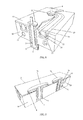
- FIGS. 8 and 9 show in cross-section view two embodiments of a plasma source integrating the device according to the invention.
- the treatment chamber comprises an amagnetic metal body ( 10 ) cooled by water circulating in a cooling circuit ( 11 ).
- a housing provided in the body receives the magnetic circuit.
- the magnetic system is formed of the first line of magnets ( 21 ) of a first polarization ( 31 ) and of the second line ( 22 ) surrounding the first line and having the opposite polarization ( 32 ).
- the two magnet lines ( 21 ) and ( 22 ) are connected by a ferromagnetic plate ( 23 ).
- the body ( 10 ) and the magnetic system are separated from the plasma by a shield ( 12 ).
- Cylindrical holes are provided in the body ( 10 ) and the sheet ( 12 ) for the microwave injection, by means of several coaxial guides having their external conductors ( 2 ) inserted into the source body in good electric contact therewith.
- the central conductor of each guide appears in the form of a cylindrical rod ( 1 ), centered with respect to the external conductor and extending beyond the shield.
- a dielectric window ( 3 ) is placed inside of the guide several centimeters away from the opening. This offset location guarantees a low fouling of the dielectric by any deposit and especially by a conductive deposit which could prevent the passing of microwaves.
- the dielectric enables to create a tightness between the inside and the outside of the vacuum treatment enclosure.
- the waveguide opening is covered with a disk ( 5 ) which prevents the deposit from penetrating into the waveguide and enables to take the microwaves to the ECR area.
- the disk ( 5 ) is topped with a rod ( 6 ) which enables to optimize the coupling with the plasma.
- the rod length has been adjusted between 16 and 35 mm for a 2.45-GHz microwave frequency and a 90-W power per antenna.
- the ease of ignition is observed.
- the ignition is considered as easy if it requires no modification at the level of the impedance matching devices located on each injection line.
- the basic design of the treatment chamber is the same. The difference lies in the antennas.
- the antenna plates ( 7 a ) and ( 7 b ) are elongated along the injector axis. Elongation ( 7 a ) is asymmetrical with respect to the central conductor ( 1 ) for an antenna which is located at one end of the plasma source, at the center of a turn of the magnetic circuit, the elongation only being towards the opposite end.
- Elongation ( 7 b ) is symmetrical with respect to the central conductor for an antenna located in the linear portion of the magnetic circuit. Each elongated portion is terminated by a short-circuit ( 8 ) avoiding for the antenna to radiate towards its neighbor.
- the width of the plate decreases as the distance from the central conductor increases ( 1 ) and towards the earth return.
- Such a configuration has first been tested with antennas for which the distance between the earth return and the central conductor of the waveguide is between 31 and 32 mm, and thus close to ⁇ /4 (30.6 mm). This has provided an increase of the current by approximately 3% with respect to the first embodiment. When this distance is taken to 34 mm, the current increases by an additional 3%, and thus by 6% with respect to the first embodiment. In both cases, the plate has a 3-mm thickness.
Landscapes
- Physics & Mathematics (AREA)
- Engineering & Computer Science (AREA)
- Plasma & Fusion (AREA)
- Chemical & Material Sciences (AREA)
- Analytical Chemistry (AREA)
- Electromagnetism (AREA)
- Spectroscopy & Molecular Physics (AREA)
- Plasma Technology (AREA)
- Chemical Vapour Deposition (AREA)
- Drying Of Semiconductors (AREA)
Applications Claiming Priority (3)
| Application Number | Priority Date | Filing Date | Title |
|---|---|---|---|
| FR1258495 | 2012-09-11 | ||
| FR1258495A FR2995493B1 (fr) | 2012-09-11 | 2012-09-11 | Dispositif pour generer un plasma presentant une etendue importante le long d'un axe par resonnance cyclotronique electronique rce a partir d'un milieu gazeux |
| PCT/FR2013/052035 WO2014041280A1 (fr) | 2012-09-11 | 2013-09-04 | Dispositif pour generer un plasma presentant une etendue importante le long d'un axe par resonnance cyclotronique electronique rce a partir d'un milieu gazeux. |
Publications (2)
| Publication Number | Publication Date |
|---|---|
| US20150214008A1 US20150214008A1 (en) | 2015-07-30 |
| US9490102B2 true US9490102B2 (en) | 2016-11-08 |
Family
ID=47902052
Family Applications (1)
| Application Number | Title | Priority Date | Filing Date |
|---|---|---|---|
| US14/425,409 Active 2033-10-23 US9490102B2 (en) | 2012-09-11 | 2013-09-04 | Device for generating plasma having a high range along an axis by electron cyclotron resonance (ECR) from a gaseous medium |
Country Status (23)
| Country | Link |
|---|---|
| US (1) | US9490102B2 (fr) |
| EP (1) | EP2896278B1 (fr) |
| JP (1) | JP6265997B2 (fr) |
| KR (1) | KR102107510B1 (fr) |
| CN (1) | CN104620682B (fr) |
| AR (1) | AR092517A1 (fr) |
| BR (1) | BR112015004624B1 (fr) |
| CA (1) | CA2883570C (fr) |
| DK (1) | DK2896278T3 (fr) |
| ES (1) | ES2742884T3 (fr) |
| FR (1) | FR2995493B1 (fr) |
| HU (1) | HUE045110T2 (fr) |
| LT (1) | LT2896278T (fr) |
| MX (1) | MX342253B (fr) |
| MY (1) | MY201589A (fr) |
| PL (1) | PL2896278T3 (fr) |
| PT (1) | PT2896278T (fr) |
| RU (1) | RU2642424C2 (fr) |
| SG (1) | SG11201501338XA (fr) |
| SI (1) | SI2896278T1 (fr) |
| TR (1) | TR201910906T4 (fr) |
| TW (1) | TWI587752B (fr) |
| WO (1) | WO2014041280A1 (fr) |
Families Citing this family (6)
| Publication number | Priority date | Publication date | Assignee | Title |
|---|---|---|---|---|
| TWI758589B (zh) * | 2018-03-01 | 2022-03-21 | 美商應用材料股份有限公司 | 電漿源組件和提供電漿的方法 |
| FR3082527B1 (fr) | 2018-06-18 | 2020-09-18 | Hydromecanique & Frottement | Piece revetue par un revetement de carbone amorphe non-hydrogene sur une sous-couche comportant du chrome, du carbone et du silicium |
| FR3082526B1 (fr) | 2018-06-18 | 2020-09-18 | Hydromecanique & Frottement | Piece revetue par un revetement de carbone amorphe hydrogene sur une sous-couche comportant du chrome, du carbone et du silicium |
| US11037765B2 (en) * | 2018-07-03 | 2021-06-15 | Tokyo Electron Limited | Resonant structure for electron cyclotron resonant (ECR) plasma ionization |
| CN111140454B (zh) * | 2020-02-13 | 2021-05-04 | 哈尔滨工业大学 | 一种微型电子回旋共振离子推力器点火装置 |
| RU2771009C1 (ru) * | 2021-06-01 | 2022-04-25 | Федеральное государственное бюджетное учреждение науки Физико-технологический институт имени К.А. Валиева Российской академии наук | Способ и устройство для повышения латеральной однородности и плотности низкотемпературной плазмы в широкоапертурных технологических реакторах микроэлектроники |
Citations (15)
| Publication number | Priority date | Publication date | Assignee | Title |
|---|---|---|---|---|
| US4610770A (en) * | 1983-12-26 | 1986-09-09 | Hitachi, Ltd. | Method and apparatus for sputtering |
| US4745337A (en) | 1985-06-07 | 1988-05-17 | Centre National D'etudes Des Telecommunications | Method and device for exciting a plasma using microwaves at the electronic cyclotronic resonance |
| US4883968A (en) * | 1988-06-03 | 1989-11-28 | Eaton Corporation | Electron cyclotron resonance ion source |
| DE4136297A1 (de) | 1991-11-04 | 1993-05-06 | Plasma Electronic Gmbh, 7024 Filderstadt, De | Vorrichtung zur lokalen erzeugung eines plasmas in einer behandlungskammer mittels mikrowellenanregung |
| US5446137A (en) * | 1993-12-09 | 1995-08-29 | Syntex (U.S.A.) Inc. | Oligonucleotides containing 4'-substituted nucleotides |
| US5587205A (en) * | 1992-12-28 | 1996-12-24 | Hitachi, Ltd. | Plasma processing method and an apparatus for carrying out the same |
| DE19812558A1 (de) | 1998-03-21 | 1999-09-30 | Roth & Rau Oberflaechentechnik | Vorrichtung zur Erzeugung linear ausgedehnter ECR-Plasmen |
| US5961773A (en) * | 1996-03-28 | 1999-10-05 | Hitachi, Ltd. | Plasma processing apparatus and plasma processing method using the same |
| EP1075168A1 (fr) | 1999-08-04 | 2001-02-07 | METAL PROCESS, Société à Responsabilité Limiteé: | Procédé de production de plasmas élémentaires en vue de créer un plasma uniforme pour une surface d'utilisation et dispositif de production d'un tel plasma |
| US20010026575A1 (en) * | 1999-12-20 | 2001-10-04 | Noriyoshi Sato | Plasma processing system |
| WO2005027595A2 (fr) | 2003-09-08 | 2005-03-24 | Roth & Rau Ag | Source de plasma ecr comprenant une ouverture de sortie de plasma lineaire |
| WO2008009558A1 (fr) | 2006-07-21 | 2008-01-24 | Centre National De La Recherche Scientifique (Cnrs) | Dispositif et procédé de production et de confinement d'un plasma |
| WO2008017304A2 (fr) | 2006-08-09 | 2008-02-14 | Roth & Rau Ag | Source de plasma ecr |
| EP1976346A1 (fr) | 2007-03-30 | 2008-10-01 | Ecole Polytechnique | Appareil de génération de plasma |
| US20100219160A1 (en) * | 2007-10-16 | 2010-09-02 | H.E.F. | Method of treating a surface of at least one part by means of individual sources of an electron cyclotron resonance plasma |
Family Cites Families (9)
| Publication number | Priority date | Publication date | Assignee | Title |
|---|---|---|---|---|
| JPH03191068A (ja) * | 1989-12-20 | 1991-08-21 | Matsushita Electric Ind Co Ltd | マイクロ波プラズマ装置 |
| DE4037091C2 (de) * | 1990-11-22 | 1996-06-20 | Leybold Ag | Vorrichtung für die Erzeugung eines homogenen Mikrowellenfeldes |
| US5283538A (en) * | 1990-11-22 | 1994-02-01 | Leybold Aktiengesellschaft | Apparatus for coupling microwave power out of a first space into a second space |
| JPH0828350B2 (ja) * | 1992-12-09 | 1996-03-21 | 雄一 坂本 | Ecr型プラズマ発生装置 |
| JPH07296991A (ja) * | 1994-04-25 | 1995-11-10 | Kokusai Electric Co Ltd | マイクロ波プラズマ発生装置 |
| FR2726729B1 (fr) * | 1994-11-04 | 1997-01-31 | Metal Process | Dispositif de production d'un plasma permettant une dissociation entre les zones de propagation et d'absorption des micro-ondes |
| JPH09186000A (ja) * | 1995-12-28 | 1997-07-15 | Anelva Corp | プラズマ処理装置 |
| JP2875221B2 (ja) * | 1996-11-15 | 1999-03-31 | ニチメン電子工研株式会社 | プラズマ発生装置 |
| JP2000306901A (ja) * | 2000-01-01 | 2000-11-02 | Hitachi Ltd | プラズマ処理装置及びプラズマ処理方法 |
-
2012
- 2012-09-11 FR FR1258495A patent/FR2995493B1/fr not_active Expired - Fee Related
-
2013
- 2013-09-04 BR BR112015004624-0A patent/BR112015004624B1/pt active IP Right Grant
- 2013-09-04 TR TR2019/10906T patent/TR201910906T4/tr unknown
- 2013-09-04 JP JP2015530475A patent/JP6265997B2/ja active Active
- 2013-09-04 ES ES13774719T patent/ES2742884T3/es active Active
- 2013-09-04 PL PL13774719T patent/PL2896278T3/pl unknown
- 2013-09-04 CN CN201380046725.8A patent/CN104620682B/zh active Active
- 2013-09-04 CA CA2883570A patent/CA2883570C/fr active Active
- 2013-09-04 KR KR1020157006130A patent/KR102107510B1/ko active Active
- 2013-09-04 US US14/425,409 patent/US9490102B2/en active Active
- 2013-09-04 WO PCT/FR2013/052035 patent/WO2014041280A1/fr not_active Ceased
- 2013-09-04 LT LTEP13774719.2T patent/LT2896278T/lt unknown
- 2013-09-04 EP EP13774719.2A patent/EP2896278B1/fr active Active
- 2013-09-04 SG SG11201501338XA patent/SG11201501338XA/en unknown
- 2013-09-04 PT PT13774719T patent/PT2896278T/pt unknown
- 2013-09-04 RU RU2015108163A patent/RU2642424C2/ru active
- 2013-09-04 MY MYPI2015700540A patent/MY201589A/en unknown
- 2013-09-04 MX MX2015003170A patent/MX342253B/es active IP Right Grant
- 2013-09-04 HU HUE13774719A patent/HUE045110T2/hu unknown
- 2013-09-04 SI SI201331536T patent/SI2896278T1/sl unknown
- 2013-09-04 DK DK13774719.2T patent/DK2896278T3/da active
- 2013-09-09 TW TW102132427A patent/TWI587752B/zh active
- 2013-09-11 AR ARP130103235A patent/AR092517A1/es active IP Right Grant
Patent Citations (18)
| Publication number | Priority date | Publication date | Assignee | Title |
|---|---|---|---|---|
| US4610770A (en) * | 1983-12-26 | 1986-09-09 | Hitachi, Ltd. | Method and apparatus for sputtering |
| US4745337A (en) | 1985-06-07 | 1988-05-17 | Centre National D'etudes Des Telecommunications | Method and device for exciting a plasma using microwaves at the electronic cyclotronic resonance |
| US4883968A (en) * | 1988-06-03 | 1989-11-28 | Eaton Corporation | Electron cyclotron resonance ion source |
| DE4136297A1 (de) | 1991-11-04 | 1993-05-06 | Plasma Electronic Gmbh, 7024 Filderstadt, De | Vorrichtung zur lokalen erzeugung eines plasmas in einer behandlungskammer mittels mikrowellenanregung |
| US5587205A (en) * | 1992-12-28 | 1996-12-24 | Hitachi, Ltd. | Plasma processing method and an apparatus for carrying out the same |
| US5446137A (en) * | 1993-12-09 | 1995-08-29 | Syntex (U.S.A.) Inc. | Oligonucleotides containing 4'-substituted nucleotides |
| US5446137B1 (en) * | 1993-12-09 | 1998-10-06 | Behringwerke Ag | Oligonucleotides containing 4'-substituted nucleotides |
| US5961773A (en) * | 1996-03-28 | 1999-10-05 | Hitachi, Ltd. | Plasma processing apparatus and plasma processing method using the same |
| DE19812558A1 (de) | 1998-03-21 | 1999-09-30 | Roth & Rau Oberflaechentechnik | Vorrichtung zur Erzeugung linear ausgedehnter ECR-Plasmen |
| EP1075168A1 (fr) | 1999-08-04 | 2001-02-07 | METAL PROCESS, Société à Responsabilité Limiteé: | Procédé de production de plasmas élémentaires en vue de créer un plasma uniforme pour une surface d'utilisation et dispositif de production d'un tel plasma |
| US20010026575A1 (en) * | 1999-12-20 | 2001-10-04 | Noriyoshi Sato | Plasma processing system |
| WO2005027595A2 (fr) | 2003-09-08 | 2005-03-24 | Roth & Rau Ag | Source de plasma ecr comprenant une ouverture de sortie de plasma lineaire |
| WO2008009558A1 (fr) | 2006-07-21 | 2008-01-24 | Centre National De La Recherche Scientifique (Cnrs) | Dispositif et procédé de production et de confinement d'un plasma |
| WO2008017304A2 (fr) | 2006-08-09 | 2008-02-14 | Roth & Rau Ag | Source de plasma ecr |
| EP1976346A1 (fr) | 2007-03-30 | 2008-10-01 | Ecole Polytechnique | Appareil de génération de plasma |
| US20100074807A1 (en) * | 2007-03-30 | 2010-03-25 | Ecole Polytechnique | Apparatus for generating a plasma |
| US20100219160A1 (en) * | 2007-10-16 | 2010-09-02 | H.E.F. | Method of treating a surface of at least one part by means of individual sources of an electron cyclotron resonance plasma |
| US8728588B2 (en) * | 2007-10-16 | 2014-05-20 | H.E.F. | Method of treating a surface of at least one part by means of individual sources of an electron cyclotron resonance plasma |
Non-Patent Citations (1)
| Title |
|---|
| International Search Report for PCT/FR2013/052035 dated Nov. 7, 2013. |
Also Published As
| Publication number | Publication date |
|---|---|
| TR201910906T4 (tr) | 2019-08-21 |
| SI2896278T1 (sl) | 2019-10-30 |
| CA2883570C (fr) | 2020-03-24 |
| KR102107510B1 (ko) | 2020-05-07 |
| KR20150053918A (ko) | 2015-05-19 |
| FR2995493B1 (fr) | 2014-08-22 |
| JP6265997B2 (ja) | 2018-01-24 |
| DK2896278T3 (da) | 2019-08-19 |
| MX2015003170A (es) | 2015-07-14 |
| AR092517A1 (es) | 2015-04-22 |
| EP2896278A1 (fr) | 2015-07-22 |
| FR2995493A1 (fr) | 2014-03-14 |
| ES2742884T3 (es) | 2020-02-17 |
| JP2015534214A (ja) | 2015-11-26 |
| HUE045110T2 (hu) | 2019-12-30 |
| RU2015108163A (ru) | 2016-09-27 |
| CN104620682A (zh) | 2015-05-13 |
| MY201589A (en) | 2024-03-02 |
| PT2896278T (pt) | 2019-07-30 |
| WO2014041280A1 (fr) | 2014-03-20 |
| CA2883570A1 (fr) | 2014-03-20 |
| SG11201501338XA (en) | 2015-04-29 |
| EP2896278B1 (fr) | 2019-06-12 |
| BR112015004624B1 (pt) | 2021-01-12 |
| PL2896278T3 (pl) | 2019-10-31 |
| TWI587752B (zh) | 2017-06-11 |
| RU2642424C2 (ru) | 2018-01-25 |
| US20150214008A1 (en) | 2015-07-30 |
| BR112015004624A2 (pt) | 2017-07-04 |
| LT2896278T (lt) | 2019-08-12 |
| CN104620682B (zh) | 2017-09-05 |
| TW201415958A (zh) | 2014-04-16 |
| MX342253B (es) | 2016-09-21 |
Similar Documents
| Publication | Publication Date | Title |
|---|---|---|
| US9490102B2 (en) | Device for generating plasma having a high range along an axis by electron cyclotron resonance (ECR) from a gaseous medium | |
| EP1058489A2 (fr) | Procédé et dispositif pour générer un plasma | |
| US20070119376A1 (en) | Matching device and plasma processing apparatus | |
| JPH0563413A (ja) | 規則的なマイクロ波の場を発生させる装置 | |
| TW201532119A (zh) | 多單元共振器微波表面波電漿設備 | |
| CN114830289A (zh) | 用于生成等离子体的方法和装置 | |
| Degeling et al. | Characterization of helicon waves in a magnetized inductive discharge | |
| KR101377469B1 (ko) | 플라즈마 처리장치 및 플라즈마 처리방법 | |
| KR101446554B1 (ko) | 다중 방전관 어셈블리를 갖는 플라즈마 챔버 | |
| WO2021152518A1 (fr) | Résonateur à micro-ondes à excitation par des ouvertures de diffraction destiné à des sources d'ions et des pièges à plasma | |
| WO2009048294A2 (fr) | Appareil de traitement au plasma couplé par induction et magnétisé et procédé de production correspondant | |
| KR102805060B1 (ko) | 공진 도파관에 의한 플라즈마 발생장치 | |
| KR101605060B1 (ko) | Ecr 플라즈마 발생장치 | |
| Kurisu et al. | Improvement of microwave feeding on a large bore ECRIS with permanent magnets by using coaxial semi-dipole antenna | |
| KR100284501B1 (ko) | 전자레인지의 슬롯 안테나 | |
| Efthimion et al. | ECR plasma source for heavy ion beam charge neutralization | |
| KR20100062715A (ko) | 상압 플라즈마 발생 장치 및 이를 이용한 상압 플라즈마 발생 방법 | |
| KR101690625B1 (ko) | 대면적 ecr 플라즈마 발생장치 | |
| KR20240151977A (ko) | 확장이 자유로운 공진 도파관에 의한 플라즈마 발생장치 | |
| Gerst et al. | Strip-like structure in a low-pressure magnetized RF discharge | |
| JP2909992B2 (ja) | マイクロ波放電反応装置 | |
| Pahlavan et al. | Frequency scanning in the uniform leaky-wave antenna based on nonradiative dielectric (NRD) waveguide | |
| Chen et al. | ECR Sources | |
| JPH04120276A (ja) | 表面処理装置 | |
| KR20180121145A (ko) | 도파관 형태의 안테나를 이용한 마이크로 웨이브 플라즈마 발생 장치 |
Legal Events
| Date | Code | Title | Description |
|---|---|---|---|
| AS | Assignment |
Owner name: H.E.F., FRANCE Free format text: ASSIGNMENT OF ASSIGNORS INTEREST;ASSIGNORS:SCHMIDT, BEAT;HEAU, CHRISTOPHE;MAURIN-PERRIER, PHILIPPE;REEL/FRAME:035075/0866 Effective date: 20150212 |
|
| STCF | Information on status: patent grant |
Free format text: PATENTED CASE |
|
| MAFP | Maintenance fee payment |
Free format text: PAYMENT OF MAINTENANCE FEE, 4TH YEAR, LARGE ENTITY (ORIGINAL EVENT CODE: M1551); ENTITY STATUS OF PATENT OWNER: LARGE ENTITY Year of fee payment: 4 |
|
| MAFP | Maintenance fee payment |
Free format text: PAYMENT OF MAINTENANCE FEE, 8TH YEAR, LARGE ENTITY (ORIGINAL EVENT CODE: M1552); ENTITY STATUS OF PATENT OWNER: LARGE ENTITY Year of fee payment: 8 |