US9521763B2 - Display device having display panel and a case that covers an edge of the display panel - Google Patents
Display device having display panel and a case that covers an edge of the display panel Download PDFInfo
- Publication number
- US9521763B2 US9521763B2 US14/537,358 US201414537358A US9521763B2 US 9521763 B2 US9521763 B2 US 9521763B2 US 201414537358 A US201414537358 A US 201414537358A US 9521763 B2 US9521763 B2 US 9521763B2
- Authority
- US
- United States
- Prior art keywords
- display panel
- case
- display device
- vertical
- horizontal
- Prior art date
- Legal status (The legal status is an assumption and is not a legal conclusion. Google has not performed a legal analysis and makes no representation as to the accuracy of the status listed.)
- Active, expires
Links
Images


Classifications
-
- G—PHYSICS
- G09—EDUCATION; CRYPTOGRAPHY; DISPLAY; ADVERTISING; SEALS
- G09F—DISPLAYING; ADVERTISING; SIGNS; LABELS OR NAME-PLATES; SEALS
- G09F9/00—Indicating arrangements for variable information in which the information is built-up on a support by selection or combination of individual elements
-
- H—ELECTRICITY
- H05—ELECTRIC TECHNIQUES NOT OTHERWISE PROVIDED FOR
- H05K—PRINTED CIRCUITS; CASINGS OR CONSTRUCTIONAL DETAILS OF ELECTRIC APPARATUS; MANUFACTURE OF ASSEMBLAGES OF ELECTRICAL COMPONENTS
- H05K5/00—Casings, cabinets or drawers for electric apparatus
- H05K5/0017—Casings, cabinets or drawers for electric apparatus with operator interface units
-
- G—PHYSICS
- G06—COMPUTING OR CALCULATING; COUNTING
- G06F—ELECTRIC DIGITAL DATA PROCESSING
- G06F1/00—Details not covered by groups G06F3/00 - G06F13/00 and G06F21/00
- G06F1/16—Constructional details or arrangements
- G06F1/1601—Constructional details related to the housing of computer displays, e.g. of CRT monitors, of flat displays
-
- G—PHYSICS
- G09—EDUCATION; CRYPTOGRAPHY; DISPLAY; ADVERTISING; SEALS
- G09F—DISPLAYING; ADVERTISING; SIGNS; LABELS OR NAME-PLATES; SEALS
- G09F9/00—Indicating arrangements for variable information in which the information is built-up on a support by selection or combination of individual elements
- G09F9/30—Indicating arrangements for variable information in which the information is built-up on a support by selection or combination of individual elements in which the desired character or characters are formed by combining individual elements
- G09F9/35—Indicating arrangements for variable information in which the information is built-up on a support by selection or combination of individual elements in which the desired character or characters are formed by combining individual elements being liquid crystals
-
- H—ELECTRICITY
- H05—ELECTRIC TECHNIQUES NOT OTHERWISE PROVIDED FOR
- H05K—PRINTED CIRCUITS; CASINGS OR CONSTRUCTIONAL DETAILS OF ELECTRIC APPARATUS; MANUFACTURE OF ASSEMBLAGES OF ELECTRICAL COMPONENTS
- H05K5/00—Casings, cabinets or drawers for electric apparatus
-
- H—ELECTRICITY
- H05—ELECTRIC TECHNIQUES NOT OTHERWISE PROVIDED FOR
- H05K—PRINTED CIRCUITS; CASINGS OR CONSTRUCTIONAL DETAILS OF ELECTRIC APPARATUS; MANUFACTURE OF ASSEMBLAGES OF ELECTRICAL COMPONENTS
- H05K5/00—Casings, cabinets or drawers for electric apparatus
- H05K5/02—Details
-
- H—ELECTRICITY
- H05—ELECTRIC TECHNIQUES NOT OTHERWISE PROVIDED FOR
- H05K—PRINTED CIRCUITS; CASINGS OR CONSTRUCTIONAL DETAILS OF ELECTRIC APPARATUS; MANUFACTURE OF ASSEMBLAGES OF ELECTRICAL COMPONENTS
- H05K5/00—Casings, cabinets or drawers for electric apparatus
- H05K5/02—Details
- H05K5/0217—Mechanical details of casings
-
- H—ELECTRICITY
- H05—ELECTRIC TECHNIQUES NOT OTHERWISE PROVIDED FOR
- H05K—PRINTED CIRCUITS; CASINGS OR CONSTRUCTIONAL DETAILS OF ELECTRIC APPARATUS; MANUFACTURE OF ASSEMBLAGES OF ELECTRICAL COMPONENTS
- H05K5/00—Casings, cabinets or drawers for electric apparatus
- H05K5/02—Details
- H05K5/03—Covers
-
- H—ELECTRICITY
- H05—ELECTRIC TECHNIQUES NOT OTHERWISE PROVIDED FOR
- H05K—PRINTED CIRCUITS; CASINGS OR CONSTRUCTIONAL DETAILS OF ELECTRIC APPARATUS; MANUFACTURE OF ASSEMBLAGES OF ELECTRICAL COMPONENTS
- H05K5/00—Casings, cabinets or drawers for electric apparatus
- H05K5/10—Casings, cabinets or drawers for electric apparatus comprising several parts forming a closed casing
-
- G—PHYSICS
- G02—OPTICS
- G02B—OPTICAL ELEMENTS, SYSTEMS OR APPARATUS
- G02B6/00—Light guides; Structural details of arrangements comprising light guides and other optical elements, e.g. couplings
- G02B6/0001—Light guides; Structural details of arrangements comprising light guides and other optical elements, e.g. couplings specially adapted for lighting devices or systems
- G02B6/0011—Light guides; Structural details of arrangements comprising light guides and other optical elements, e.g. couplings specially adapted for lighting devices or systems the light guides being planar or of plate-like form
- G02B6/0081—Mechanical or electrical aspects of the light guide and light source in the lighting device peculiar to the adaptation to planar light guides, e.g. concerning packaging
- G02B6/0086—Positioning aspects
- G02B6/0091—Positioning aspects of the light source relative to the light guide
-
- G—PHYSICS
- G02—OPTICS
- G02F—OPTICAL DEVICES OR ARRANGEMENTS FOR THE CONTROL OF LIGHT BY MODIFICATION OF THE OPTICAL PROPERTIES OF THE MEDIA OF THE ELEMENTS INVOLVED THEREIN; NON-LINEAR OPTICS; FREQUENCY-CHANGING OF LIGHT; OPTICAL LOGIC ELEMENTS; OPTICAL ANALOGUE/DIGITAL CONVERTERS
- G02F1/00—Devices or arrangements for the control of the intensity, colour, phase, polarisation or direction of light arriving from an independent light source, e.g. switching, gating or modulating; Non-linear optics
- G02F1/01—Devices or arrangements for the control of the intensity, colour, phase, polarisation or direction of light arriving from an independent light source, e.g. switching, gating or modulating; Non-linear optics for the control of the intensity, phase, polarisation or colour
- G02F1/13—Devices or arrangements for the control of the intensity, colour, phase, polarisation or direction of light arriving from an independent light source, e.g. switching, gating or modulating; Non-linear optics for the control of the intensity, phase, polarisation or colour based on liquid crystals, e.g. single liquid crystal display cells
- G02F1/133—Constructional arrangements; Operation of liquid crystal cells; Circuit arrangements
- G02F1/1333—Constructional arrangements; Manufacturing methods
- G02F1/133308—Support structures for LCD panels, e.g. frames or bezels
- G02F1/133314—Back frames
-
- G—PHYSICS
- G02—OPTICS
- G02F—OPTICAL DEVICES OR ARRANGEMENTS FOR THE CONTROL OF LIGHT BY MODIFICATION OF THE OPTICAL PROPERTIES OF THE MEDIA OF THE ELEMENTS INVOLVED THEREIN; NON-LINEAR OPTICS; FREQUENCY-CHANGING OF LIGHT; OPTICAL LOGIC ELEMENTS; OPTICAL ANALOGUE/DIGITAL CONVERTERS
- G02F1/00—Devices or arrangements for the control of the intensity, colour, phase, polarisation or direction of light arriving from an independent light source, e.g. switching, gating or modulating; Non-linear optics
- G02F1/01—Devices or arrangements for the control of the intensity, colour, phase, polarisation or direction of light arriving from an independent light source, e.g. switching, gating or modulating; Non-linear optics for the control of the intensity, phase, polarisation or colour
- G02F1/13—Devices or arrangements for the control of the intensity, colour, phase, polarisation or direction of light arriving from an independent light source, e.g. switching, gating or modulating; Non-linear optics for the control of the intensity, phase, polarisation or colour based on liquid crystals, e.g. single liquid crystal display cells
- G02F1/133—Constructional arrangements; Operation of liquid crystal cells; Circuit arrangements
- G02F1/1333—Constructional arrangements; Manufacturing methods
- G02F1/133308—Support structures for LCD panels, e.g. frames or bezels
- G02F1/13332—Front frames
-
- G—PHYSICS
- G02—OPTICS
- G02F—OPTICAL DEVICES OR ARRANGEMENTS FOR THE CONTROL OF LIGHT BY MODIFICATION OF THE OPTICAL PROPERTIES OF THE MEDIA OF THE ELEMENTS INVOLVED THEREIN; NON-LINEAR OPTICS; FREQUENCY-CHANGING OF LIGHT; OPTICAL LOGIC ELEMENTS; OPTICAL ANALOGUE/DIGITAL CONVERTERS
- G02F1/00—Devices or arrangements for the control of the intensity, colour, phase, polarisation or direction of light arriving from an independent light source, e.g. switching, gating or modulating; Non-linear optics
- G02F1/01—Devices or arrangements for the control of the intensity, colour, phase, polarisation or direction of light arriving from an independent light source, e.g. switching, gating or modulating; Non-linear optics for the control of the intensity, phase, polarisation or colour
- G02F1/13—Devices or arrangements for the control of the intensity, colour, phase, polarisation or direction of light arriving from an independent light source, e.g. switching, gating or modulating; Non-linear optics for the control of the intensity, phase, polarisation or colour based on liquid crystals, e.g. single liquid crystal display cells
- G02F1/133—Constructional arrangements; Operation of liquid crystal cells; Circuit arrangements
- G02F1/1333—Constructional arrangements; Manufacturing methods
- G02F1/133308—Support structures for LCD panels, e.g. frames or bezels
- G02F1/133325—Assembling processes
-
- G—PHYSICS
- G02—OPTICS
- G02F—OPTICAL DEVICES OR ARRANGEMENTS FOR THE CONTROL OF LIGHT BY MODIFICATION OF THE OPTICAL PROPERTIES OF THE MEDIA OF THE ELEMENTS INVOLVED THEREIN; NON-LINEAR OPTICS; FREQUENCY-CHANGING OF LIGHT; OPTICAL LOGIC ELEMENTS; OPTICAL ANALOGUE/DIGITAL CONVERTERS
- G02F1/00—Devices or arrangements for the control of the intensity, colour, phase, polarisation or direction of light arriving from an independent light source, e.g. switching, gating or modulating; Non-linear optics
- G02F1/01—Devices or arrangements for the control of the intensity, colour, phase, polarisation or direction of light arriving from an independent light source, e.g. switching, gating or modulating; Non-linear optics for the control of the intensity, phase, polarisation or colour
- G02F1/13—Devices or arrangements for the control of the intensity, colour, phase, polarisation or direction of light arriving from an independent light source, e.g. switching, gating or modulating; Non-linear optics for the control of the intensity, phase, polarisation or colour based on liquid crystals, e.g. single liquid crystal display cells
- G02F1/133—Constructional arrangements; Operation of liquid crystal cells; Circuit arrangements
- G02F1/1333—Constructional arrangements; Manufacturing methods
- G02F1/133308—Support structures for LCD panels, e.g. frames or bezels
- G02F1/133328—Segmented frames
-
- G02F2001/13332—
-
- G02F2001/133325—
-
- G02F2001/133328—
-
- G—PHYSICS
- G02—OPTICS
- G02F—OPTICAL DEVICES OR ARRANGEMENTS FOR THE CONTROL OF LIGHT BY MODIFICATION OF THE OPTICAL PROPERTIES OF THE MEDIA OF THE ELEMENTS INVOLVED THEREIN; NON-LINEAR OPTICS; FREQUENCY-CHANGING OF LIGHT; OPTICAL LOGIC ELEMENTS; OPTICAL ANALOGUE/DIGITAL CONVERTERS
- G02F2201/00—Constructional arrangements not provided for in groups G02F1/00 - G02F7/00
- G02F2201/46—Fixing elements
-
- H—ELECTRICITY
- H04—ELECTRIC COMMUNICATION TECHNIQUE
- H04N—PICTORIAL COMMUNICATION, e.g. TELEVISION
- H04N5/00—Details of television systems
- H04N5/64—Constructional details of receivers, e.g. cabinets or dust covers
Definitions
- Embodiments of the disclosure relate to a display device.
- a liquid crystal display panel of the liquid crystal display includes a liquid crystal layer, and a thin film transistor (TFT) substrate and a color filter substrate which are positioned opposite each other with the liquid crystal layer interposed therebetween.
- TFT thin film transistor
- the liquid crystal display panel displays an image using light provided by a backlight unit of the liquid crystal display.
- Display devices have various types of enclosures or cases. Display devices having improved cases that reduces unnecessary use of materials is desired.
- FIGS. 1 and 2 schematically illustrate configuration of a display device according to an exemplary embodiment of the disclosure
- FIGS. 3 to 16 illustrate a front case
- FIGS. 17 to 22 illustrate a guide panel
- FIGS. 23 to 46 illustrate in detail configuration of a display device according to an exemplary embodiment of the disclosure.
- first ‘first’, ‘second’, etc. may be used to describe various components, but the components are not limited by such terms. The terms are used only for the purpose of distinguishing one component from other components.
- a first component may be designated as a second component without departing from the scope of the present disclosure.
- the second component may be designated as the first component.
- a liquid crystal display panel is used as an example of a display panel.
- Other display panels may be used.
- a plasma display panel (PDP), a field emission display (FED) panel, and an organic light emitting display panel may be used.
- a first direction DR 1 may be a direction parallel to long sides LS 1 and LS 2 of a display panel 420
- a second direction DR 2 may be a direction parallel to short sides SS 1 and SS 2 of the display panel 420 .
- a third direction DR 3 may be a direction vertical to the first direction DR 1 and/or the second direction DR 2 .
- the first direction DR 1 and the second direction DR 2 may be commonly referred to as a horizontal direction.
- the third direction DR 3 may be referred to as a vertical direction.
- FIGS. 1 and 2 schematically illustrate configuration of a display device according to an exemplary embodiment of the disclosure.
- a display device 100 may include a display panel 420 , a top case 410 , and a back cabinet 460 .
- the top case 410 may also be referred to herein as a front case or a front cover.
- the back cabinet 460 may also be referred to herein as a bottom cabinet or bottom cover.
- the display panel 420 displaying an image may include a front substrate and a back substrate, which are positioned opposite each other.
- the top case 410 may cover an edge of a front surface of the display panel 420 . More specifically, the display panel 420 may include a first long side LS 1 , a second long side LS 2 opposite the first long side LS 1 , a first short side SS 1 adjacent to the first long side LS 1 and the second long side LS 2 , and a second short side SS 2 opposite the first short side SS 1 .
- the top case 410 may cover the edge of the front surface of the display panel 420 on all of the first and second long sides LS 1 and LS 2 and the first and second short sides SS 1 and SS 2 .
- the top case 410 may be divided into a plurality of parts. The top case 410 is described in detail below.
- the back cabinet 460 may be disposed in the rear of the display panel 420 and may protect various parts positioned between the display panel 420 and the back cabinet 460 .
- a back cover 450 may be disposed between the display panel 420 and the back cabinet 460 .
- Various parts including a driving board (for example, a printed circuit board), light sources (not shown), etc. may be disposed on the back cover 450 .
- a light guide plate 440 may be disposed between the back cover 450 and the display panel 420 . As described above, when the light guide plate 440 is disposed, an edge type backlight unit, in which the light sources are positioned on the side of the light guide plate 440 , may be applied to the embodiment of the disclosure.
- a direct type backlight unit in which the light sources are positioned under the display panel 420 , may be applied to the embodiment of the disclosure.
- An optical layer (not shown) may be disposed between the light guide plate 440 and the display panel 420 .
- a guide panel 430 may be disposed in the rear of the display panel 420 .
- a fastening member 470 may fasten the back cover 450 to the back cabinet 460 .
- the top case 410 , the display panel 420 , the guide panel 430 , the light guide plate 440 , and the back cover 450 (or bottom cover) may be included in a display module 100 M.
- the display module 100 M may further include the optical layer, the light sources, and the like.
- FIGS. 3 to 16 illustrate the top case 410 .
- duplicative descriptions of the configuration and the structure described above may be briefly made or may be entirely omitted.
- the top case 410 may include horizontal top cases 410 H 1 and 410 H 2 covering an edge of the front surface of the display panel 420 on the long sides LS 1 and LS 2 of the display panel 420 and vertical top cases 410 V 1 and 410 V 2 covering an edge of the front surface of the display panel 420 on the short sides SS 1 and SS 2 of the display panel 420 .
- the horizontal top cases 410 H 1 and 410 H 2 may include a first horizontal top case 410 H 1 corresponding to the first long side LS 1 of the display panel 420 and a second horizontal top case 410 H 2 corresponding to the second long side LS 2 of the display panel 420 .
- the vertical top cases 410 V 1 and 410 V 2 may include a first vertical top case 410 V 1 corresponding to the first short side SS 1 of the display panel 420 and a second vertical top case 410 V 2 corresponding to the second short side SS 2 of the display panel 420 .
- the horizontal top cases 410 H 1 and 410 H 2 and the vertical top cases 410 V 1 and 410 V 2 may be connected on the corner of the display panel 420 .
- the first horizontal top case 410 H 1 and the first vertical top case 410 V 1 may be connected to each other on the corner of the first long side LS 1 and the first short side SS 1 of the display panel 420 .
- the first horizontal top case 410 H 1 and the second vertical top case 410 V 2 may be connected to each other on the corner of the first long side LS 1 and the second short side SS 2 of the display panel 420 .
- the second horizontal top case 410 H 2 and the first vertical top case 410 V 1 may be connected to each other on the corner of the second long side LS 2 and the first short side SS 1 of the display panel 420 .
- the second horizontal top case 410 H 2 and the second vertical top case 410 V 2 may be connected to each other on the corner of the second long side LS 2 and the second short side SS 2 of the display panel 420 .
- each of the horizontal top cases 410 H 1 and 410 H 2 may include a first part 500 , a second part 510 connected to the first part 500 , and a third part 520 connected to the second part 510 .
- the first part 500 may extend in the second direction DR 2 of the horizontal direction (i.e., the first direction DR 1 and/or the second direction DR 2 ) and may include a portion covering an edge of the front surface of the display panel 420 on the long sides LS 1 and LS 2 of the display panel 420 .
- the second part 510 may extend from a first end E 1 of the first part 500 and may include a portion positioned on the side of the display panel 420 on the long sides LS 1 and LS 2 of the display panel 420 .
- the third part 520 may extend from an end of the second part 510 in the second direction DR 2 of the horizontal direction (i.e., the first direction DR 1 and/or the second direction DR 2 ).
- Each of the horizontal top cases 410 H 1 and 410 H 2 may further include a fourth part 530 connected to the first part 500 and a sixth part 550 connected to the third part 520 .
- the fourth part 530 may extend from a second end E 2 opposite the first end E 1 of the first part 500 in the vertical direction (i.e., the third direction DR 3 ) and may be positioned on the front surface of the display panel 420 on the long sides LS 1 and LS 2 of the display panel 420 .
- the sixth part 550 may extend from the third part 520 in the vertical direction (i.e., the third direction DR 3 ).
- the second part 510 may include a portion having a surface bending in an oblique direction.
- the second part 510 may include a surface which extends from the first part 500 in the oblique direction and convexly bends.
- each of the horizontal top cases 410 H 1 and 410 H 2 may have a first wall thickness T 1 .
- each of the horizontal top cases 410 H 1 and 410 H 2 may further include a fifth part 540 .
- the fifth part 540 may extend from the fourth part 530 in the second direction DR 2 of the horizontal direction (i.e., the first direction DR 1 and/or the second direction DR 2 ).
- the fifth part 540 may be used to connect the horizontal top cases 410 H 1 and 410 H 2 with the vertical top cases 410 V 1 and 410 V 2 .
- the fifth part 540 may have a variety of shapes and may be referred to herein as a tab or protrusion.
- each of the horizontal top cases 410 H 1 and 410 H 2 may have a first hole H 1 through which a fastening member passes.
- the first hole H 1 may be used to connect the horizontal top cases 410 H 1 and 410 H 2 with another structure, for example, the vertical top cases 410 V 1 and 410 V 2 and/or the guide panel 430 .
- the sixth part 550 may be omitted in both end areas W 1 of each of the horizontal top cases 410 H 1 and 410 H 2 . That is, a length of the sixth part 550 in the first direction DR 1 may be less than a length of the first part 500 . As described above, when the sixth part 550 is omitted in the end areas W 1 of the horizontal top cases 410 H 1 and 410 H 2 , the horizontal top cases 410 H 1 and 410 H 2 and the vertical top cases 410 V 1 and 410 V 2 may be easily connected on the corners of the display panel 420 .
- the horizontal top case 410 H 1 , 410 H 2 covers an edge on the front surface of the display panel.
- the first part 500 may be referred to as a front surface
- the second part 510 may be referred to as a lateral surface
- the third part 520 may be referred to as a rear surface.
- the fourth part 530 may be referred to as a flange.
- the fifth part 540 may be referred to as a tab, flange or protrusion.
- the sixth part 550 may be referred to as a flange.
- each of the vertical top cases 410 V 1 and 410 V 2 may include a first part 600 (also referred to as a horizontal part) and a second part 610 (also referred to herein as a vertical part) connected to the first part 600 .
- the first part 600 may be referred to as a front surface and the second part 610 may be referred to as a lateral surface of the vertical case.
- the first part 600 may extend in the first direction DR 1 of the horizontal direction (i.e., the first direction DR 1 and/or the second direction DR 2 ) and may include a portion covering an edge of the front surface of the display panel 420 on the short sides SS 1 and SS 2 of the display panel 420 .
- the second part 610 may extend from the first part 600 and may include a portion positioned on the side of the display panel 420 on the short sides SS 1 and SS 2 of the display panel 420 .
- Each of the vertical top cases 410 V 1 and 410 V 2 may further include a first auxiliary part 620 extending from the second part 610 in the first direction DR 1 of the horizontal direction (i.e., the first direction DR 1 and/or the second direction DR 2 ) and a second auxiliary part 630 extending from the first auxiliary part 620 in the vertical direction (i.e., the third direction DR 3 ).
- each of the vertical top cases 410 V 1 and 410 V 2 may have a second wall thickness T 2 .
- the second part 610 of each of the vertical top cases 410 V 1 and 410 V 2 may include an extension 640 which extends further than the first part 600 by a predetermined height W 2 in the second direction DR 2 of the horizontal direction (i.e., the first direction DR 1 and/or the second direction DR 2 ).
- Each of the vertical top cases 410 V 1 and 410 V 2 may further include an overlap part 650 (also referred to herein as a protrusion) extending from the extension 640 in the first direction DR 1 of the horizontal direction (i.e., the first direction DR 1 and/or the second direction DR 2 ).
- the overlap part 650 may include a connection part 660 (also referred to herein as a tab) which extends in the vertical direction (i.e., the third direction DR 3 ) and has a second hole H 2 .
- the second hole H 2 may correspond to the first hole H 1 .
- the horizontal top cases 410 H 1 and 410 H 2 and the vertical top cases 410 V 1 and 410 V 2 may be connected on the corners of the display panel 420 .
- the fifth part 540 of the horizontal top cases 410 H 1 and 410 H 2 may be inserted into a lower part of the first part 600 of the vertical top cases 410 V 1 and 410 V 2 .
- a first fastening member S 100 such as a screw, may pass through the first hole H 1 and the second hole H 2 and may connect the horizontal top cases 410 H 1 and 410 H 2 with the vertical top cases 410 V 1 and 410 V 2 .
- the fifth part 540 of the horizontal top cases 410 H 1 and 410 H 2 may be covered by the first part 600 of the vertical top cases 410 V 1 and 410 V 2 .
- the overlap part 650 of the vertical top cases 410 V 1 and 410 V 2 may be covered by the horizontal top cases 410 H 1 and 410 H 2 .
- the fifth part 540 of the horizontal top cases 410 H 1 and 410 H 2 may be inserted into a lower part of the first part 600 of the vertical top cases 410 V 1 and 410 V 2 .
- the horizontal top cases 410 H 1 and 410 H 2 may cover the edge of the front surface of the display panel 420 on the long sides LS 1 and LS 2 of the display panel 420
- the vertical top cases 410 V 1 and 410 V 2 may cover the edge of the front surface of the display panel 420 on the short sides SS 1 and SS 2 of the display panel 420 .
- the horizontal top cases 410 H 1 and 410 H 2 and the vertical top cases 410 V 1 and 410 V 2 may be aligned by the fifth parts 540 of the horizontal top cases 410 H 1 and 410 H 2 and the overlap parts 650 of the vertical top cases 410 V 1 and 410 V 2 .
- the first wall thickness T 1 of the horizontal top cases 410 H 1 and 410 H 2 may be less than the second wall thickness T 2 of the vertical top cases 410 V 1 and 410 V 2 .
- the horizontal top cases 410 H 1 and 410 H 2 and the vertical top cases 410 V 1 and 410 V 2 may be formed of different materials.
- the horizontal top cases 410 H 1 and 410 H 2 may contain a metal material
- the vertical top cases 410 V 1 and 410 V 2 may contain a plastic material.
- top case 410 A reason to divide the top case 410 into the horizontal top cases 410 H 1 and 410 H 2 and the vertical top cases 410 V 1 and 410 V 2 formed of different materials is described below.
- a mother metal plate 700 may be processed through a press working method to manufacture a top case.
- a middle portion 710 of the mother metal plate 700 may be removed along a predetermined cutting line CL in a press working process.
- an outer portion 720 positioned outside the middle portion 710 of the mother metal plate 700 may be used as the top case.
- the manufacturing cost of the display device may increase due to the unnecessary waste of material.
- the first horizontal top case 410 H 1 , the second horizontal top case 410 H 2 , the first vertical top case 410 V 1 , and the second vertical top case 410 V 2 may be individually manufactured. Therefore, the unnecessary waste of material may be reduced. Hence, the manufacturing cost of the display device may be reduced.
- Paint or tape may be applied to a surface of at least one of the first part 600 and the second part 610 of each of the vertical top cases 410 V 1 and 410 V 2 , so as to match surface colors of the horizontal top cases 410 H 1 and 410 H 2 and the vertical top cases 410 V 1 and 410 V 2 .
- a silver paint or a silver tape may be applied to the surface of at least one of the first part 600 and the second part 610 of each of the vertical top cases 410 V 1 and 410 V 2 , and thus the vertical top cases 410 V 1 and 410 V 2 may appear to have a metal surface that matches the horizontal top cases 410 H 1 and 410 H 2 .
- a cover 800 containing a metal material may be disposed on the surface of at least one of the first part 600 and the second part 610 of each of the vertical top cases 410 V 1 and 410 V 2 .
- FIGS. 17 to 22 illustrate the guide panel.
- the descriptions of the configuration and the structure described above may be briefly made or may be entirely omitted.
- the guide panel 430 may include a base part 900 and a side wall 910 connected to the base part 900 .
- the base part 900 may extend in the horizontal direction (i.e., the first direction DR 1 and/or the second direction DR 2 ).
- the base part 900 may be attached to a back surface of the display panel 420 through an adhesive layer 1000 .
- a groove 902 to which the adhesive layer 1000 is applied, may be formed on a bottom surface (i.e., a first surface S 1 ) of the base part 900 .
- a protrusion 901 protruding in the vertical direction i.e., the third direction DR 3
- an upper surface i.e., a second surface S 2
- the guide panel 430 may further include an inner wall 920 .
- the inner wall 920 may be positioned between the side wall 910 and the protrusion 901 .
- the inner wall 920 may extend from the upper surface S 2 of the base part 900 in the vertical direction (i.e., the third direction DR 3 ).
- the side wall 910 may include a forward part 912 extending forward from the base part 900 in the vertical direction (i.e., the third direction DR 3 ) and a backward part 911 extending backwards from the base part 900 in the vertical direction (i.e., the third direction DR 3 ).
- a length W 4 of the backward part 911 may be longer than a length W 5 of the forward part 912 .
- the length W 4 of the backward part 911 of the side wall 910 may be longer than a length of the inner wall 920 by a predetermined length W 3 .
- a first end E 1 of the side wall 910 is one end of the backward part 911
- a second end E 2 of the side wall 910 is one end of the forward part 912 .
- the other end of the backward part 911 and the other end of the forward part 912 may be connected to each other.
- the groove 902 is formed on the bottom surface S 1 of the guide panel 430 .
- the forward part 912 of the side wall 910 of the guide panel 430 may include a guide part 903 protruding in the horizontal direction (i.e., the first direction DR 1 and/or the second direction DR 2 ).
- the guide part 903 may prevent the side of the display panel 420 from colliding with the forward part 912 of the side wall 910 .
- a buffer 904 with elasticity may be disposed between the guide part 903 and the side of the display panel 420 .
- the buffer 904 may be formed of a material with elasticity, for example, a resin material.
- the guide panel 430 may include a plurality of inner walls 920 which are positioned to be separated from one another in the horizontal direction (i.e., the first direction DR 1 and/or the second direction DR 2 ).
- the side wall 910 may be also divided into a plurality of parts. Namely, the plurality of side walls 910 may be positioned to be separated from one another in the horizontal direction (i.e., the first direction DR 1 and/or the second direction DR 2 ).
- a space between the side walls 910 positioned adjacent in the horizontal direction (i.e., the first direction DR 1 and/or the second direction DR 2 ) may be referred to as a path 930 .
- At least one path 930 may overlap the inner wall 920 .
- the guide panel 430 may further include a first hook HK 1 protruding from an external surface EXS of the side wall 910 in the horizontal direction (i.e., the first direction DR 1 and/or the second direction DR 2 ).
- the first hook HK 1 may correspond to a predetermined hole of the top case 410 .
- each of the vertical top cases 410 V 1 and 410 V 2 may have a third hole H 3 corresponding to the first hook HK 1 .
- FIGS. 23 to 46 illustrate in detail configuration of the display device according to the embodiment of the disclosure.
- the descriptions of the configuration and the structure described above may be briefly made or may be entirely omitted.
- the display device 100 may include an optical layer 1100 and the light guide plate 440 .
- the optical layer 1100 may include a plurality of sheets.
- the optical layer 1100 may include a diffusion sheet 1110 and a prism sheet 1120 .
- the optical layer 1100 may be disposed on the base part 900 of the guide panel 430 . More specifically, the optical layer 1100 may be disposed on the protrusion 901 of the base part 900 of the guide panel 430 .
- the protrusion 901 may reduce an area of a contact surface between the optical layer 1100 and the guide panel 430 .
- An air gap of a predetermined width Z 1 may be formed between the optical layer 1100 and the display panel 420 in the vertical direction (i.e., the third direction DR 3 ).
- the back cover 450 may be disposed in the rear of the optical layer 1100 .
- the back cover 450 may be placed on the inner wall 920 of the guide panel 430 .
- the back cover 450 may be connected to the side wall 910 of the guide panel 430 through a predetermined second fastening member S 200 .
- a method for connecting the back cover 450 with the guide panel 430 is not limited thereto.
- the back cabinet 460 may be disposed in the rear of the back cover 450 , and the top case 410 covering the edge of the front surface of the display panel 420 may be disposed.
- the top case 410 may cover the side wall 910 of the guide panel 430 on the side of the display device 100 .
- the back cover 450 may include a horizontal frame part 451 extending in the horizontal direction (i.e., the first direction DR 1 and/or the second direction DR 2 ) and an inclined part 454 which extends from the horizontal frame part 451 in an oblique direction. Further, the back cover 450 may include an upward part 452 protruding backwards from an end of the back cover 450 in the vertical direction (i.e., the third direction DR 3 ) and a downward part 453 protruding forward from the end of the back cover 450 in the vertical direction (i.e., the third direction DR 3 ).
- the downward part 453 may be disposed between the side wall 910 and the inner wall 920 of the guide panel 430 .
- the top case 410 may be separated from an end of the back cabinet 460 by a predetermined distance Z 2 in the vertical direction (i.e., the third direction DR 3 ) in a state where the top case 410 and the back cabinet 460 are installed.
- the third parts 520 of the horizontal top cases 410 H 1 and 410 H 2 may be separated from the end of the back cabinet 460 by the predetermined distance Z 2 in the vertical direction (i.e., the third direction DR 3 ).
- At least one of the horizontal top cases 410 H 1 and 410 H 2 and the vertical top cases 410 V 1 and 410 V 2 may extend further than the back cabinet 460 by a predetermined length W 6 in the horizontal direction (i.e., the first direction DR 1 and/or the second direction DR 2 ).
- the back cabinet 460 may be connected to the back cover 450 .
- the back cover 450 may include a supporter 455 protruding toward the back cabinet 460 .
- the supporter 455 may have a fourth hole H 4 .
- the supporter 455 may be formed on the inclined part 454 of the back cover 450
- the back cabinet 460 may have a fifth hole H 5 corresponding to the fourth hole H 4 .
- a fastening member 470 such as a screw, may pass through the fifth hole H 5 and the fourth hole H 4 and may fasten the back cabinet 460 to the back cover 450 .
- the back cover 450 when the back cover 450 includes the supporter 455 protruding toward the back cabinet 460 and the back cabinet 460 is fastened to the back cover 450 using the supporter 455 , a fastening position between the back cover 450 and the back cabinet 460 may approach the outside of the display device. Hence, an increase in a thickness of the display device resulting from the fastening between the back cover 450 and the back cabinet 460 while more strongly fastening the back cabinet 460 to the back cover 450 may be suppressed.
- a protrusion 1200 may be formed at an edge of the back cabinet 460 to maintain a distance between the end of the back cabinet 460 and the end of the back cover 450 .
- the protrusion 1200 of the back cabinet 460 may protrude from an inner surface of the back cabinet 460 toward the back cover 450 in the vertical direction (i.e., the third direction DR 3 ).
- the guide panel 430 may include a hanging part 940 extending from the external surface EXS of the first end E 1 of the side wall 910 in the horizontal direction (i.e., the first direction DR 1 and/or the second direction DR 2 ). An end of the top case 410 may hang on the hanging part 940 of the guide panel 430 .
- the top case 410 may be connected to the back cover 450 .
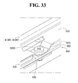
- the sixth part 550 of each of the horizontal top cases 410 H 1 and 410 H 2 may have a seventh hole H 7
- the back cover 450 may have a sixth hole H 6 corresponding to the seventh hole H 7
- the upward part 452 of the back cover 450 may have the sixth hole H 6 .
- a predetermined third fastening member S 300 may pass through the seventh hole H 7 and the sixth hole H 6 and may fasten the horizontal top cases 410 H 1 and 410 H 2 to the back cover 450 . More specifically, as shown in FIG. 33 , the third fastening member S 300 may fasten the horizontal top cases 410 H 1 and 410 H 2 to the back cover 450 through the path 930 of the side wall 910 of the guide panel 430 .
- the horizontal top cases 410 H 1 and 410 H 2 , the vertical top cases 410 V 1 and 410 V 2 , and the back cover 450 may be connected to one another.
- the back cover 450 may have an eighth hole H 8 .
- the upward part 452 of the back cover 450 may have the eighth hole H 8 .
- the first fastening member S 100 may pass through the first holes H 1 of the horizontal top cases 410 H 1 and 410 H 2 , the second holes H 2 of the vertical top cases 410 V 1 and 410 V 2 , and the eighth hole H 8 of the back cover 450 and may fasten the horizontal top cases 410 H 1 and 410 H 2 , the vertical top cases 410 V 1 and 410 V 2 , and the back cover 450 .
- the horizontal top cases 410 H 1 and 410 H 2 , the vertical top cases 410 V 1 and 410 V 2 , and the back cover 450 may be fastened by the first fastening member S 100 .
- the guide panel 430 may include protrusions 1300 and 1310 extending from the side wall 910 in the horizontal direction (i.e., the first direction DR 1 and/or the second direction DR 2 ). More specifically, the protrusions 1300 and 1310 may extend from the external surface EXS of the side wall 910 of the guide panel 430 in the horizontal direction (i.e., the first direction DR 1 and/or the second direction DR 2 ).
- the protrusions 1300 and 1310 may include a first protrusion 1300 and a second protrusion 1310 which are separated from each other by a predetermined distance D 1 in the direction parallel to the long side LS of the display panel 420 , i.e., in the first direction DR 1 of the horizontal direction (i.e., the first direction DR 1 and/or the second direction DR 2 ).
- the sixth part 550 of each of the horizontal top cases 410 H 1 and 410 H 2 may have a first opening OP 1 corresponding to the first protrusion 1300 and a second opening OP 2 corresponding to the second protrusion 1310 .
- the first protrusion 1300 of the guide panel 430 may be inserted into the first opening OP 1 of each of the horizontal top cases 410 H 1 and 410 H 2
- the second protrusion 1310 of the guide panel 430 may be inserted into the second opening OP 2 .
- a distance D 2 between the third part 520 of each of the horizontal top cases 410 H 1 and 410 H 2 and the first protrusion 1300 in the vertical direction may be different from a distance D 3 between the third part 520 and the second protrusion 1310 .
- the distance D 2 between the third part 520 of each of the horizontal top cases 410 H 1 and 410 H 2 and the first protrusion 1300 in the vertical direction i.e., the third direction DR 3
- the end of the back cabinet 460 may be positioned between the third part 520 and the first protrusion 1300 or between the third part 520 and the second protrusion 1310 .
- an end EP 1 of the back cabinet 460 may be positioned between the third part 520 and the first protrusion 1300 .
- the wall thickness of the back cabinet 460 may be a third wall thickness T 3 which is relatively small.
- the end of the back cabinet 460 may at least contain a metal material.
- the back cabinet 460 When the back cabinet 460 is formed of the metal material, the back cabinet 460 may be manufactured using the press working method. Hence, the wall thickness T 3 of the back cabinet 460 may be relatively small.
- the end EP 1 of the back cabinet 460 positioned in the rear of the display module 100 M may hang on a protrusion extending from the side of the display module 100 M in the horizontal direction (i.e., the first direction DR 1 and/or the second direction DR 2 ).
- an end EP 2 of the back cabinet 460 may be positioned between the third part 520 and the second protrusion 1310 .
- the wall thickness of the back cabinet 460 may be a fourth wall thickness T 4 greater than the third wall thickness T 3 .
- the end of the back cabinet 460 may at least contain a plastic material.
- the back cabinet 460 When the back cabinet 460 is formed of the plastic material, the back cabinet 460 may be manufactured using the mold working method. Hence, the wall thickness T 4 of the back cabinet 460 may be relatively large.
- the back cabinet 460 has another protrusion 1400 at its end, so as to insert the back cabinet 460 having the relatively large wall thickness T 4 between the third part 520 and the second protrusion 1310 .
- the protrusion 1400 may protrude from the end of the back cabinet 460 in the first direction DR 1 .
- At least one of the horizontal top cases 410 H 1 and 410 H 2 and the vertical top cases 410 V 1 and 410 V 2 may be exposed at the corner of the display device 100 .
- (B) is a cross-sectional view of the display device 100 taken along line B 1 -B 2 of (A). Configuration shown in (B) of FIG. 43 was described in detail above.
- FIG. 44 (A) is a cross-sectional view of the display device 100 taken along line B 3 -B 4 of (B) on the first long side LS 1 of the display device 100 . Configuration shown in (A) of FIG. 44 was described in detail above.
- FIG. 44 is a cross-sectional view of the display device 100 taken along line B 3 -B 4 of (B) on the second long side LS 2 of the display device 100 .
- a structure 1500 for the support may be disposed between the back cover 450 and the back cabinet 460 on the second long side LS 2 of the display device 100 .
- a driving board (for example, a printed circuit board) 1510 and a flexible substrate 1520 may be disposed between the back cover 450 and the back cabinet 460 on the second long side LS 2 of the display device 100 .
- the flexible substrate 1520 may transmit a driving signal received from the driving board 1510 to the display panel 420 .
- a lower cover 1600 may be disposed between the back cover 450 and the back cabinet 460 on the second long side LS 2 of the display device 100 .
- one end of the lower cover 1600 may be disposed between the second horizontal top case and 410 H 2 and the guide panel 430 .
- the sixth part 550 of the second horizontal top case and 410 H 2 may have an eighth hole H 8 .
- the guide panel 430 may have a second hook HK 2 inserted into the eighth hole H 8 of the second horizontal top case and 410 H 2 .
- the guide panel 430 may further have a third hook HK 3 for firmly fixing the lower cover 1600 at an end of its side wall 910 .
- the adhesive layer 1000 for attaching the guide panel 430 to the back surface of the display panel 420 may include a base layer 1010 , a first layer 1020 which is formed on a first surface FS of the base layer 1010 and has the adhesion, and a second layer 1030 which is formed on a second surface RS of the base layer 1010 and has the adhesion.
- the base layer 1010 may be formed of a material having elasticity.
- the base layer 1010 may be formed of urethane foam.
- the adhesive layer 1000 having the above-described configuration may have the elasticity and the flexibility as well as the adhesion. Hence, the adhesive layer 1000 may prevent an external force from being applied to the guide panel 430 and thus may prevent the external force from being transferred to the display panel 420 .
- the adhesive layer 1000 having the above-described configuration may be referred to as a foam pad.
- a display device which may include a display panel, a back cabinet disposed in the rear of the display panel, and a top case configured to cover an edge of a front surface of the display panel, wherein the top case includes a horizontal top case covering an edge of the front surface of the display panel on a long side of the display panel and a vertical top case covering an edge of the front surface of the display panel on a short side of the display panel, wherein the horizontal top case and the vertical top case are connected to each other on the corner of the display panel, wherein the horizontal top case and the vertical top case are formed of different materials.
- the horizontal top case may contain a metal material
- the vertical top case may contain a plastic material.
- the horizontal top case may include a first part configured to extend in a horizontal direction, the first part including a portion covering the edge of the front surface of the display panel on the long side of the display panel, a second part configured to extend from a first end of the first part, the second part including a portion positioned on the side of the display panel on the long side of the display panel, and a third part configured to extend from an end of the second part in the horizontal direction.
- the vertical top case may include a horizontal part configured to extend in the horizontal direction, the horizontal part including a portion covering the edge of the front surface of the display panel on the short side of the display panel, and a vertical part configured to extend from the horizontal part, the vertical part including a portion positioned on the side of the display panel on the short side of the display panel.
- the horizontal top case may further include a fourth part which extends from a second end opposite the first end of the first part in a vertical direction and is positioned on the front surface of the display panel on the long side of the display panel, and a fifth part which extends from the fourth part in the horizontal direction and is covered by the horizontal part of the vertical top case.
- the horizontal top case may further include a sixth part configured to extend from the third part in the vertical direction, and the sixth part of the horizontal top case may have a first hole, through which a fastening member passes.
- the vertical part of the vertical top case may include an extension extending further than the horizontal part in the horizontal direction.
- the vertical top case may further include an overlap part which extends from the extension in the horizontal direction and is covered by the horizontal top case.
- the overlap part of the vertical top case may include a connection part which extends in the vertical direction and has a second hole corresponding to the first hole.
- the display device may further comprise a back cover positioned between the back cabinet and the display panel.
- the back cabinet may be connected to the back cover.
- At least one of the horizontal top case and the vertical top case may extend further than the back cabinet in the horizontal direction.
- the third part of the horizontal top case may be separated from the back cabinet by a predetermined distance in the vertical direction. Moreover, a paint or a tape may be applied to a surface of at least one of the horizontal part and the vertical part of the vertical top case.
- the embodiments of the disclosure can reduce the material unnecessarily consumed and thus can reduce the manufacturing cost of the display device.
- any reference in this specification to “one embodiment,” “an embodiment,” “example embodiment,” etc. means that a particular feature, structure, or characteristic described in connection with the embodiment is included in at least one embodiment of the invention.
- the appearances of such phrases in various places in the specification are not necessarily all referring to the same embodiment.
Landscapes
- Engineering & Computer Science (AREA)
- Microelectronics & Electronic Packaging (AREA)
- Theoretical Computer Science (AREA)
- General Engineering & Computer Science (AREA)
- Physics & Mathematics (AREA)
- General Physics & Mathematics (AREA)
- Computer Hardware Design (AREA)
- Human Computer Interaction (AREA)
- Chemical & Material Sciences (AREA)
- Crystallography & Structural Chemistry (AREA)
- Devices For Indicating Variable Information By Combining Individual Elements (AREA)
- Liquid Crystal (AREA)
Priority Applications (3)
| Application Number | Priority Date | Filing Date | Title |
|---|---|---|---|
| US15/352,742 US10064294B2 (en) | 2014-01-22 | 2016-11-16 | Display device having display panel and a case that covers an edge of the display panel |
| US15/655,467 US10194542B2 (en) | 2014-01-22 | 2017-07-20 | Display device having display panel and a case that covers an edge of the display panel |
| US16/018,341 US10681825B2 (en) | 2014-01-22 | 2018-06-26 | Display device having display panel and a case that covers an edge of the display panel |
Applications Claiming Priority (2)
| Application Number | Priority Date | Filing Date | Title |
|---|---|---|---|
| KR10-2014-0008003 | 2014-01-22 | ||
| KR1020140008003A KR102145892B1 (ko) | 2014-01-22 | 2014-01-22 | 디스플레이 장치 |
Related Child Applications (1)
| Application Number | Title | Priority Date | Filing Date |
|---|---|---|---|
| US15/352,742 Continuation US10064294B2 (en) | 2014-01-22 | 2016-11-16 | Display device having display panel and a case that covers an edge of the display panel |
Publications (2)
| Publication Number | Publication Date |
|---|---|
| US20150208523A1 US20150208523A1 (en) | 2015-07-23 |
| US9521763B2 true US9521763B2 (en) | 2016-12-13 |
Family
ID=52003594
Family Applications (4)
| Application Number | Title | Priority Date | Filing Date |
|---|---|---|---|
| US14/537,358 Active 2035-01-08 US9521763B2 (en) | 2014-01-22 | 2014-11-10 | Display device having display panel and a case that covers an edge of the display panel |
| US15/352,742 Active US10064294B2 (en) | 2014-01-22 | 2016-11-16 | Display device having display panel and a case that covers an edge of the display panel |
| US15/655,467 Active US10194542B2 (en) | 2014-01-22 | 2017-07-20 | Display device having display panel and a case that covers an edge of the display panel |
| US16/018,341 Active US10681825B2 (en) | 2014-01-22 | 2018-06-26 | Display device having display panel and a case that covers an edge of the display panel |
Family Applications After (3)
| Application Number | Title | Priority Date | Filing Date |
|---|---|---|---|
| US15/352,742 Active US10064294B2 (en) | 2014-01-22 | 2016-11-16 | Display device having display panel and a case that covers an edge of the display panel |
| US15/655,467 Active US10194542B2 (en) | 2014-01-22 | 2017-07-20 | Display device having display panel and a case that covers an edge of the display panel |
| US16/018,341 Active US10681825B2 (en) | 2014-01-22 | 2018-06-26 | Display device having display panel and a case that covers an edge of the display panel |
Country Status (4)
| Country | Link |
|---|---|
| US (4) | US9521763B2 (fr) |
| EP (6) | EP4271147B1 (fr) |
| KR (1) | KR102145892B1 (fr) |
| CN (2) | CN104794992B (fr) |
Cited By (2)
| Publication number | Priority date | Publication date | Assignee | Title |
|---|---|---|---|---|
| US20180138669A1 (en) * | 2016-01-22 | 2018-05-17 | Eaton Corporation | Enclosure, and window assembly and assembling method therefor |
| US20190179193A1 (en) * | 2017-12-11 | 2019-06-13 | Lg Display Co., Ltd. | Back Cover and Display Device Including the Same |
Families Citing this family (28)
| Publication number | Priority date | Publication date | Assignee | Title |
|---|---|---|---|---|
| WO2015140865A1 (fr) * | 2014-03-19 | 2015-09-24 | 株式会社Joled | Appareil d'affichage et procédé de fabrication d'un appareil d'affichage |
| EP3133907A1 (fr) * | 2014-04-14 | 2017-02-22 | Mitsubishi Electric Corporation | Boîtier |
| US20160174398A1 (en) * | 2014-12-16 | 2016-06-16 | Kabushiki Kaisha Toshiba | Electronic apparatus |
| CN104820305B (zh) * | 2015-05-19 | 2018-12-11 | 深圳市华星光电技术有限公司 | 显示装置 |
| JP6215867B2 (ja) * | 2015-05-22 | 2017-10-18 | ミネベアミツミ株式会社 | 面状照明装置 |
| KR102562961B1 (ko) * | 2015-12-08 | 2023-08-02 | 엘지디스플레이 주식회사 | 디스플레이 패널용 케이스 및 이를 포함하는 디스플레이 장치 |
| KR101718141B1 (ko) * | 2016-02-16 | 2017-03-21 | 제이에스엘씨디(주) | 프레임 어셈블리를 구비한 디스플레이 장치 |
| KR20170117307A (ko) * | 2016-03-18 | 2017-10-23 | 르 홀딩스(베이징)씨오., 엘티디. | 베젤, 디스플레이 모듈 및 디스플레이 디바이스 |
| CN105842892A (zh) * | 2016-03-18 | 2016-08-10 | 乐视致新电子科技(天津)有限公司 | 一种前框、显示模组及显示设备 |
| KR102504803B1 (ko) | 2016-04-06 | 2023-02-28 | 엘지전자 주식회사 | 디스플레이 디바이스 |
| CN205880454U (zh) * | 2016-08-04 | 2017-01-11 | 扬升照明股份有限公司 | 背光模组及显示装置 |
| US10459266B2 (en) * | 2016-08-04 | 2019-10-29 | Boe Technology Group Co., Ltd. | Display module, display apparatus having the same, and fabricating method thereof |
| KR102575466B1 (ko) * | 2016-12-13 | 2023-09-06 | 엘지디스플레이 주식회사 | 표시장치 |
| DE102017204600A1 (de) * | 2017-03-20 | 2018-09-20 | Robert Bosch Gmbh | Verbinder zum Verbinden von zwei Gehäuseteilen und Gehäuse umfassend zwei Gehäuseteile und mindestens einen Verbinder |
| KR102370820B1 (ko) | 2017-08-22 | 2022-03-07 | 엘지전자 주식회사 | 디스플레이 디바이스 |
| KR20190049987A (ko) * | 2017-11-01 | 2019-05-10 | 삼성디스플레이 주식회사 | 표시 장치 |
| CN208283685U (zh) * | 2018-04-04 | 2018-12-25 | 京东方科技集团股份有限公司 | 一种显示设备的前框组装结构及显示设备 |
| CN110880274B (zh) * | 2018-09-06 | 2021-09-21 | 纬联电子科技(中山)有限公司 | 薄型窄框的显示器以及其外框件 |
| CN109257554B (zh) * | 2018-10-30 | 2021-06-15 | 泰洋光电(惠州)有限公司 | 一种液晶电视机一体式金属背板拼接结构 |
| US11683893B2 (en) * | 2018-12-27 | 2023-06-20 | Saturn Licensing Llc | Display apparatus |
| CN109887426A (zh) * | 2019-01-25 | 2019-06-14 | 南京巨鲨显示科技有限公司 | 一种医用便携式显示器信号线接口固定结构 |
| CN109629478B (zh) * | 2019-02-02 | 2024-12-20 | 湖南湘旭交安光电高科技股份有限公司 | 一种可组合的用于道路交通标志的框架型材 |
| US10835035B1 (en) * | 2019-09-10 | 2020-11-17 | Chen-Source Inc. | Accommodation cabinet with handtoollessly assembled frame body |
| KR102680252B1 (ko) * | 2019-12-31 | 2024-07-01 | 엘지디스플레이 주식회사 | 표시장치 |
| CN111182747B (zh) * | 2020-01-02 | 2021-10-08 | 高创(苏州)电子有限公司 | 后壳安装结构及显示设备 |
| JP7457573B2 (ja) * | 2020-05-20 | 2024-03-28 | シャープ株式会社 | 表示装置 |
| CN112346546A (zh) * | 2020-11-03 | 2021-02-09 | 武汉东湖学院 | 一种计算机用防护装置 |
| JP7792596B2 (ja) * | 2022-07-14 | 2025-12-26 | パナソニックIpマネジメント株式会社 | 電子機器 |
Citations (10)
| Publication number | Priority date | Publication date | Assignee | Title |
|---|---|---|---|---|
| US6181390B1 (en) | 1999-01-27 | 2001-01-30 | Compal Electronics, Inc. | Display holder with multiple side frames |
| US20050162583A1 (en) * | 2002-09-03 | 2005-07-28 | Bloomberg Lp | Bezel-less electronic display |
| US20070090247A1 (en) | 2005-09-30 | 2007-04-26 | Hon Hai Precision Industry Co., Ltd. | Lcd panel mounting apparatus |
| US20070097330A1 (en) * | 2005-11-02 | 2007-05-03 | Lg Electronics, Inc. | Display device, cabinet assembly for the display device and method of assembling the display device |
| US20100296022A1 (en) * | 2009-05-25 | 2010-11-25 | Satoshi Ando | Liquid crystal module |
| WO2013153941A1 (fr) | 2012-04-11 | 2013-10-17 | シャープ株式会社 | Dispositif d'affichage et téléviseur |
| US20130313017A1 (en) * | 2012-05-25 | 2013-11-28 | Fih (Hong Kong) Limited | Housing and electronic device using the housing |
| US20140254192A1 (en) * | 2013-03-08 | 2014-09-11 | Honghae DO | Display device |
| US20150015793A1 (en) * | 2011-12-27 | 2015-01-15 | Sharp Kabushiki Kaisha | Display device and television receiver |
| US20150373857A1 (en) * | 2012-06-25 | 2015-12-24 | Sharp Kabushiki Kaisha | Display apparatus and television receiver |
Family Cites Families (28)
| Publication number | Priority date | Publication date | Assignee | Title |
|---|---|---|---|---|
| TW445386B (en) * | 1998-03-16 | 2001-07-11 | Hitachi Ltd | Thin-type display |
| JP5061277B2 (ja) | 2005-11-21 | 2012-10-31 | 株式会社ジャパンディスプレイイースト | 表示装置 |
| KR101195227B1 (ko) * | 2005-12-14 | 2012-10-29 | 삼성디스플레이 주식회사 | 액정 표시 장치 |
| JP4896619B2 (ja) | 2006-08-07 | 2012-03-14 | 株式会社 日立ディスプレイズ | 表示装置 |
| JP5142586B2 (ja) | 2007-05-11 | 2013-02-13 | 三菱電機株式会社 | 表示装置 |
| CN101952643B (zh) * | 2008-02-19 | 2012-09-05 | 夏普株式会社 | 照明装置、显示装置和电视接收装置 |
| CN101833185A (zh) * | 2009-03-11 | 2010-09-15 | 华映视讯(吴江)有限公司 | 光学触控式液晶显示装置 |
| WO2012042797A1 (fr) * | 2010-09-28 | 2012-04-05 | パナソニック株式会社 | Dispositif d'affichage |
| US8851695B2 (en) | 2010-10-27 | 2014-10-07 | Lg Electronics Inc. | Display apparatus |
| US9235240B2 (en) | 2010-11-11 | 2016-01-12 | Apple Inc. | Insert molding around glass members for portable electronic devices |
| WO2013018398A1 (fr) | 2011-08-01 | 2013-02-07 | シャープ株式会社 | Dispositif d'affichage mince |
| US9621838B2 (en) | 2011-10-25 | 2017-04-11 | Funai Electric Co., Ltd. | Display device and television apparatus |
| CN102692741B (zh) * | 2012-06-08 | 2015-09-09 | 深圳市华星光电技术有限公司 | 一种液晶显示模组及液晶显示装置 |
| JP5567174B2 (ja) * | 2012-06-22 | 2014-08-06 | シャープ株式会社 | 表示装置及びテレビジョン受信機 |
| KR20140008003A (ko) | 2012-07-10 | 2014-01-21 | 주식회사 네오위즈인터넷 | 카드 게임을 제공하는 방법, 서버 및 장치 |
| CN102830544B (zh) | 2012-08-28 | 2015-09-30 | 深圳市华星光电技术有限公司 | 液晶显示装置及其背光模组和框架单元 |
| WO2014034487A1 (fr) * | 2012-08-28 | 2014-03-06 | シャープ株式会社 | Appareil d'éclairage, appareil d'affichage, et récepteur de télévision |
| CN102819131B (zh) * | 2012-08-31 | 2015-04-22 | 深圳市华星光电技术有限公司 | 一种液晶显示模组及液晶显示装置 |
| CN202916557U (zh) | 2012-08-31 | 2013-05-01 | 深圳市华星光电技术有限公司 | 液晶显示模组及液晶显示装置 |
| US9030642B2 (en) | 2012-09-11 | 2015-05-12 | Shenzhen China Star Optoelectronics Technology Co., Ltd. | Liquid crystal display device |
| US20140139778A1 (en) | 2012-11-22 | 2014-05-22 | Shenzhen China Star Optoelectronics Technology Co.,Ltd. | Middle Frame and Liquid Crystal Display Device |
| CN103018935B (zh) | 2012-12-12 | 2015-07-15 | 京东方科技集团股份有限公司 | 一种边框组件及液晶显示装置 |
| EP3064988A1 (fr) | 2012-12-20 | 2016-09-07 | LG Electronics, Inc. | Dispositif d'affichage |
| TWI534505B (zh) | 2012-12-24 | 2016-05-21 | Lg顯示器股份有限公司 | 液晶顯示裝置 |
| JP2014154931A (ja) | 2013-02-05 | 2014-08-25 | Funai Electric Co Ltd | 表示装置 |
| CN103235427B (zh) * | 2013-05-06 | 2016-11-23 | 深圳市华星光电技术有限公司 | 一种液晶显示器及其窄边框结构 |
| US20140333869A1 (en) | 2013-05-09 | 2014-11-13 | Shenzhen China Star Optoelectronics Technology Co. Ltd. | Structure For Adjusting Gap Between Liquid Crystal Module and Middle Frame, And Liquid Crystal Display Device |
| JP6163875B2 (ja) * | 2013-05-23 | 2017-07-19 | 船井電機株式会社 | 表示装置 |
-
2014
- 2014-01-22 KR KR1020140008003A patent/KR102145892B1/ko active Active
- 2014-11-10 US US14/537,358 patent/US9521763B2/en active Active
- 2014-11-26 EP EP23177278.1A patent/EP4271147B1/fr active Active
- 2014-11-26 EP EP21192924.5A patent/EP3933493B1/fr active Active
- 2014-11-26 EP EP17190750.4A patent/EP3276403B1/fr active Active
- 2014-11-26 EP EP24183797.0A patent/EP4412413B1/fr active Active
- 2014-11-26 EP EP19168131.1A patent/EP3540502B1/fr active Active
- 2014-11-26 EP EP14194869.5A patent/EP2899586B1/fr active Active
-
2015
- 2015-01-08 CN CN201510007941.2A patent/CN104794992B/zh active Active
- 2015-01-08 CN CN201710846418.8A patent/CN107705726B/zh active Active
-
2016
- 2016-11-16 US US15/352,742 patent/US10064294B2/en active Active
-
2017
- 2017-07-20 US US15/655,467 patent/US10194542B2/en active Active
-
2018
- 2018-06-26 US US16/018,341 patent/US10681825B2/en active Active
Patent Citations (12)
| Publication number | Priority date | Publication date | Assignee | Title |
|---|---|---|---|---|
| US6181390B1 (en) | 1999-01-27 | 2001-01-30 | Compal Electronics, Inc. | Display holder with multiple side frames |
| US20050162583A1 (en) * | 2002-09-03 | 2005-07-28 | Bloomberg Lp | Bezel-less electronic display |
| US20070090247A1 (en) | 2005-09-30 | 2007-04-26 | Hon Hai Precision Industry Co., Ltd. | Lcd panel mounting apparatus |
| US20070097330A1 (en) * | 2005-11-02 | 2007-05-03 | Lg Electronics, Inc. | Display device, cabinet assembly for the display device and method of assembling the display device |
| EP1783583A1 (fr) | 2005-11-02 | 2007-05-09 | LG Electronics Inc. | Boîtier pour un affichage à cristaux liquides de grand dimension et procédé d'assemblage associé |
| US20100296022A1 (en) * | 2009-05-25 | 2010-11-25 | Satoshi Ando | Liquid crystal module |
| EP2256539A2 (fr) | 2009-05-25 | 2010-12-01 | Funai Electric Co., Ltd. | Module à cristaux liquides |
| US20150015793A1 (en) * | 2011-12-27 | 2015-01-15 | Sharp Kabushiki Kaisha | Display device and television receiver |
| WO2013153941A1 (fr) | 2012-04-11 | 2013-10-17 | シャープ株式会社 | Dispositif d'affichage et téléviseur |
| US20130313017A1 (en) * | 2012-05-25 | 2013-11-28 | Fih (Hong Kong) Limited | Housing and electronic device using the housing |
| US20150373857A1 (en) * | 2012-06-25 | 2015-12-24 | Sharp Kabushiki Kaisha | Display apparatus and television receiver |
| US20140254192A1 (en) * | 2013-03-08 | 2014-09-11 | Honghae DO | Display device |
Non-Patent Citations (1)
| Title |
|---|
| European Search Report issued in Application No. 14194869.5 dated Jun. 8, 2015. |
Cited By (4)
| Publication number | Priority date | Publication date | Assignee | Title |
|---|---|---|---|---|
| US20180138669A1 (en) * | 2016-01-22 | 2018-05-17 | Eaton Corporation | Enclosure, and window assembly and assembling method therefor |
| US10170896B2 (en) * | 2016-01-22 | 2019-01-01 | Eaton Intelligent Power Limited | Enclosure, and window assembly and assembling method therefor |
| US20190179193A1 (en) * | 2017-12-11 | 2019-06-13 | Lg Display Co., Ltd. | Back Cover and Display Device Including the Same |
| US10564457B2 (en) * | 2017-12-11 | 2020-02-18 | Lg Display Co., Ltd. | Back cover and display device including the same |
Also Published As
| Publication number | Publication date |
|---|---|
| EP4412413C0 (fr) | 2025-11-05 |
| EP4412413B1 (fr) | 2025-11-05 |
| EP4412413A3 (fr) | 2024-10-23 |
| EP4271147B1 (fr) | 2024-08-21 |
| CN107705726B (zh) | 2020-09-08 |
| EP4271147C0 (fr) | 2024-08-21 |
| EP2899586B1 (fr) | 2017-09-27 |
| US10681825B2 (en) | 2020-06-09 |
| US20180302996A1 (en) | 2018-10-18 |
| US20150208523A1 (en) | 2015-07-23 |
| EP3933493B1 (fr) | 2023-06-07 |
| EP3276403A3 (fr) | 2018-05-09 |
| EP3276403A2 (fr) | 2018-01-31 |
| EP3276403B1 (fr) | 2019-05-22 |
| US10194542B2 (en) | 2019-01-29 |
| EP4412413A2 (fr) | 2024-08-07 |
| CN107705726A (zh) | 2018-02-16 |
| US20170071065A1 (en) | 2017-03-09 |
| EP2899586A1 (fr) | 2015-07-29 |
| EP4271147A3 (fr) | 2024-01-03 |
| EP3540502A2 (fr) | 2019-09-18 |
| EP3933493A1 (fr) | 2022-01-05 |
| EP3540502A3 (fr) | 2019-11-13 |
| CN104794992B (zh) | 2017-10-24 |
| US10064294B2 (en) | 2018-08-28 |
| EP3540502B1 (fr) | 2021-11-17 |
| EP4271147A2 (fr) | 2023-11-01 |
| US20170318695A1 (en) | 2017-11-02 |
| CN104794992A (zh) | 2015-07-22 |
| KR20150087739A (ko) | 2015-07-30 |
| EP3933493C0 (fr) | 2023-06-07 |
| KR102145892B1 (ko) | 2020-08-19 |
Similar Documents
| Publication | Publication Date | Title |
|---|---|---|
| US10681825B2 (en) | Display device having display panel and a case that covers an edge of the display panel | |
| US20220104379A1 (en) | Display apparatus | |
| US9516771B2 (en) | Display device comprising a film part which covers a display module | |
| US9655258B2 (en) | Display device | |
| US20120182700A1 (en) | Display apparatus | |
| KR102163702B1 (ko) | 디스플레이 장치 | |
| JP2010134004A (ja) | 表示装置 | |
| US20170227808A1 (en) | Display device | |
| EP2607946B1 (fr) | Appareil d'affichage | |
| US9658649B2 (en) | Display device and laptop computer | |
| US20140078413A1 (en) | Liquid crystal display structure | |
| KR102218037B1 (ko) | 디스플레이 장치 |
Legal Events
| Date | Code | Title | Description |
|---|---|---|---|
| AS | Assignment |
Owner name: LG ELECTRONICS INC., KOREA, REPUBLIC OF Free format text: ASSIGNMENT OF ASSIGNORS INTEREST;ASSIGNORS:LEE, JEIN;KANG, SEUNGGYU;LEE, JAEHUN;AND OTHERS;REEL/FRAME:034138/0266 Effective date: 20141106 |
|
| STCF | Information on status: patent grant |
Free format text: PATENTED CASE |
|
| FEPP | Fee payment procedure |
Free format text: PAYOR NUMBER ASSIGNED (ORIGINAL EVENT CODE: ASPN); ENTITY STATUS OF PATENT OWNER: LARGE ENTITY |
|
| MAFP | Maintenance fee payment |
Free format text: PAYMENT OF MAINTENANCE FEE, 4TH YEAR, LARGE ENTITY (ORIGINAL EVENT CODE: M1551); ENTITY STATUS OF PATENT OWNER: LARGE ENTITY Year of fee payment: 4 |
|
| MAFP | Maintenance fee payment |
Free format text: PAYMENT OF MAINTENANCE FEE, 8TH YEAR, LARGE ENTITY (ORIGINAL EVENT CODE: M1552); ENTITY STATUS OF PATENT OWNER: LARGE ENTITY Year of fee payment: 8 |