US9613986B2 - Array substrate and its manufacturing method, display device - Google Patents
Array substrate and its manufacturing method, display device Download PDFInfo
- Publication number
- US9613986B2 US9613986B2 US14/388,182 US201314388182A US9613986B2 US 9613986 B2 US9613986 B2 US 9613986B2 US 201314388182 A US201314388182 A US 201314388182A US 9613986 B2 US9613986 B2 US 9613986B2
- Authority
- US
- United States
- Prior art keywords
- layer
- pattern
- gate
- electrode
- data
- Prior art date
- Legal status (The legal status is an assumption and is not a legal conclusion. Google has not performed a legal analysis and makes no representation as to the accuracy of the status listed.)
- Expired - Fee Related, expires
Links
Images


Classifications
-
- H01L27/124—
-
- H01L27/1222—
-
- H01L27/1288—
-
- H01L29/78642—
-
- H—ELECTRICITY
- H10—SEMICONDUCTOR DEVICES; ELECTRIC SOLID-STATE DEVICES NOT OTHERWISE PROVIDED FOR
- H10D—INORGANIC ELECTRIC SEMICONDUCTOR DEVICES
- H10D30/00—Field-effect transistors [FET]
- H10D30/60—Insulated-gate field-effect transistors [IGFET]
- H10D30/67—Thin-film transistors [TFT]
- H10D30/6728—Vertical TFTs
-
- H—ELECTRICITY
- H10—SEMICONDUCTOR DEVICES; ELECTRIC SOLID-STATE DEVICES NOT OTHERWISE PROVIDED FOR
- H10D—INORGANIC ELECTRIC SEMICONDUCTOR DEVICES
- H10D30/00—Field-effect transistors [FET]
- H10D30/60—Insulated-gate field-effect transistors [IGFET]
- H10D30/67—Thin-film transistors [TFT]
- H10D30/6729—Thin-film transistors [TFT] characterised by the electrodes
- H10D30/673—Thin-film transistors [TFT] characterised by the electrodes characterised by the shapes, relative sizes or dispositions of the gate electrodes
-
- H—ELECTRICITY
- H10—SEMICONDUCTOR DEVICES; ELECTRIC SOLID-STATE DEVICES NOT OTHERWISE PROVIDED FOR
- H10D—INORGANIC ELECTRIC SEMICONDUCTOR DEVICES
- H10D86/00—Integrated devices formed in or on insulating or conducting substrates, e.g. formed in silicon-on-insulator [SOI] substrates or on stainless steel or glass substrates
- H10D86/01—Manufacture or treatment
- H10D86/021—Manufacture or treatment of multiple TFTs
- H10D86/0231—Manufacture or treatment of multiple TFTs using masks, e.g. half-tone masks
-
- H—ELECTRICITY
- H10—SEMICONDUCTOR DEVICES; ELECTRIC SOLID-STATE DEVICES NOT OTHERWISE PROVIDED FOR
- H10D—INORGANIC ELECTRIC SEMICONDUCTOR DEVICES
- H10D86/00—Integrated devices formed in or on insulating or conducting substrates, e.g. formed in silicon-on-insulator [SOI] substrates or on stainless steel or glass substrates
- H10D86/40—Integrated devices formed in or on insulating or conducting substrates, e.g. formed in silicon-on-insulator [SOI] substrates or on stainless steel or glass substrates characterised by multiple TFTs
- H10D86/421—Integrated devices formed in or on insulating or conducting substrates, e.g. formed in silicon-on-insulator [SOI] substrates or on stainless steel or glass substrates characterised by multiple TFTs having a particular composition, shape or crystalline structure of the active layer
-
- H—ELECTRICITY
- H10—SEMICONDUCTOR DEVICES; ELECTRIC SOLID-STATE DEVICES NOT OTHERWISE PROVIDED FOR
- H10D—INORGANIC ELECTRIC SEMICONDUCTOR DEVICES
- H10D86/00—Integrated devices formed in or on insulating or conducting substrates, e.g. formed in silicon-on-insulator [SOI] substrates or on stainless steel or glass substrates
- H10D86/40—Integrated devices formed in or on insulating or conducting substrates, e.g. formed in silicon-on-insulator [SOI] substrates or on stainless steel or glass substrates characterised by multiple TFTs
- H10D86/441—Interconnections, e.g. scanning lines
-
- H—ELECTRICITY
- H10—SEMICONDUCTOR DEVICES; ELECTRIC SOLID-STATE DEVICES NOT OTHERWISE PROVIDED FOR
- H10D—INORGANIC ELECTRIC SEMICONDUCTOR DEVICES
- H10D86/00—Integrated devices formed in or on insulating or conducting substrates, e.g. formed in silicon-on-insulator [SOI] substrates or on stainless steel or glass substrates
- H10D86/40—Integrated devices formed in or on insulating or conducting substrates, e.g. formed in silicon-on-insulator [SOI] substrates or on stainless steel or glass substrates characterised by multiple TFTs
- H10D86/60—Integrated devices formed in or on insulating or conducting substrates, e.g. formed in silicon-on-insulator [SOI] substrates or on stainless steel or glass substrates characterised by multiple TFTs wherein the TFTs are in active matrices
-
- G—PHYSICS
- G02—OPTICS
- G02F—OPTICAL DEVICES OR ARRANGEMENTS FOR THE CONTROL OF LIGHT BY MODIFICATION OF THE OPTICAL PROPERTIES OF THE MEDIA OF THE ELEMENTS INVOLVED THEREIN; NON-LINEAR OPTICS; FREQUENCY-CHANGING OF LIGHT; OPTICAL LOGIC ELEMENTS; OPTICAL ANALOGUE/DIGITAL CONVERTERS
- G02F1/00—Devices or arrangements for the control of the intensity, colour, phase, polarisation or direction of light arriving from an independent light source, e.g. switching, gating or modulating; Non-linear optics
- G02F1/01—Devices or arrangements for the control of the intensity, colour, phase, polarisation or direction of light arriving from an independent light source, e.g. switching, gating or modulating; Non-linear optics for the control of the intensity, phase, polarisation or colour
- G02F1/13—Devices or arrangements for the control of the intensity, colour, phase, polarisation or direction of light arriving from an independent light source, e.g. switching, gating or modulating; Non-linear optics for the control of the intensity, phase, polarisation or colour based on liquid crystals, e.g. single liquid crystal display cells
- G02F1/133—Constructional arrangements; Operation of liquid crystal cells; Circuit arrangements
- G02F1/1333—Constructional arrangements; Manufacturing methods
- G02F1/1343—Electrodes
- G02F1/134309—Electrodes characterised by their geometrical arrangement
- G02F1/134372—Electrodes characterised by their geometrical arrangement for fringe field switching [FFS] where the common electrode is not patterned
-
- G—PHYSICS
- G02—OPTICS
- G02F—OPTICAL DEVICES OR ARRANGEMENTS FOR THE CONTROL OF LIGHT BY MODIFICATION OF THE OPTICAL PROPERTIES OF THE MEDIA OF THE ELEMENTS INVOLVED THEREIN; NON-LINEAR OPTICS; FREQUENCY-CHANGING OF LIGHT; OPTICAL LOGIC ELEMENTS; OPTICAL ANALOGUE/DIGITAL CONVERTERS
- G02F1/00—Devices or arrangements for the control of the intensity, colour, phase, polarisation or direction of light arriving from an independent light source, e.g. switching, gating or modulating; Non-linear optics
- G02F1/01—Devices or arrangements for the control of the intensity, colour, phase, polarisation or direction of light arriving from an independent light source, e.g. switching, gating or modulating; Non-linear optics for the control of the intensity, phase, polarisation or colour
- G02F1/13—Devices or arrangements for the control of the intensity, colour, phase, polarisation or direction of light arriving from an independent light source, e.g. switching, gating or modulating; Non-linear optics for the control of the intensity, phase, polarisation or colour based on liquid crystals, e.g. single liquid crystal display cells
- G02F1/133—Constructional arrangements; Operation of liquid crystal cells; Circuit arrangements
- G02F1/136—Liquid crystal cells structurally associated with a semi-conducting layer or substrate, e.g. cells forming part of an integrated circuit
- G02F1/1362—Active matrix addressed cells
- G02F1/136286—Wiring, e.g. gate line, drain line
-
- G—PHYSICS
- G02—OPTICS
- G02F—OPTICAL DEVICES OR ARRANGEMENTS FOR THE CONTROL OF LIGHT BY MODIFICATION OF THE OPTICAL PROPERTIES OF THE MEDIA OF THE ELEMENTS INVOLVED THEREIN; NON-LINEAR OPTICS; FREQUENCY-CHANGING OF LIGHT; OPTICAL LOGIC ELEMENTS; OPTICAL ANALOGUE/DIGITAL CONVERTERS
- G02F1/00—Devices or arrangements for the control of the intensity, colour, phase, polarisation or direction of light arriving from an independent light source, e.g. switching, gating or modulating; Non-linear optics
- G02F1/01—Devices or arrangements for the control of the intensity, colour, phase, polarisation or direction of light arriving from an independent light source, e.g. switching, gating or modulating; Non-linear optics for the control of the intensity, phase, polarisation or colour
- G02F1/13—Devices or arrangements for the control of the intensity, colour, phase, polarisation or direction of light arriving from an independent light source, e.g. switching, gating or modulating; Non-linear optics for the control of the intensity, phase, polarisation or colour based on liquid crystals, e.g. single liquid crystal display cells
- G02F1/133—Constructional arrangements; Operation of liquid crystal cells; Circuit arrangements
- G02F1/136—Liquid crystal cells structurally associated with a semi-conducting layer or substrate, e.g. cells forming part of an integrated circuit
- G02F1/1362—Active matrix addressed cells
- G02F1/1368—Active matrix addressed cells in which the switching element is a three-electrode device
-
- G02F2001/134372—
Definitions
- Embodiments of the present invention relate to an array substrate and its manufacturing method, and a display device.
- a thin film transistor liquid crystal display (TFT-LCD) has the advantages such as small size, low power consumption, free of radiation, and so on, and plays a leading role in the flat panel display area.
- LCDs can be divided into various types according to different electric field forms.
- An advanced-super dimension switch (short for ADS) type TFT-LCD has wide viewing angle, high aperture ratio, high transmittance and the like advantages and thus is widely applied.
- An ADS type is a planar electric-field wide-viewing-angle technology, and its core technology properties are described as below: a multi-dimensional electric field is formed by an electric field generated at edges of slit electrodes that are in a same plane and an electric field generated between a slit electrode layer and a plate-like electrode layer, so that the liquid crystal molecules at all orientation between the slit electrodes and over the electrodes in a liquid crystal cell rotate can be subjected to rotations, and thus the work efficiency of liquid crystal and the light transmittance are increased.
- An ADS type switching technology can increase the picture quality of a TFT-LCD product, and has the advantages of high resolution ratio, high transmittance, low power consumption, wide viewing angle, high aperture ratio, low color difference, free of push mura, and so on.
- the improvements in the ADS technology comprise high transmittance I-ADS technology, high aperture ratio H-ADS, high resolution ratio S-ADS technology, and so on.
- Embodiments of the present invention provide an array substrate and its manufacturing method, and a display device.
- the array substrate reduces the channel length of the conducting channel of a thin film transistor unit, and meanwhile increases the aperture ratio of a pixel; and the manufacturing method can reduce the manufacturing difficulty of an array substrate, decrease the manufacturing costs, and increase the yield.
- An aspect of the present invention provides an array substrate, which comprises: a base substrate and a thin film transistor unit provided on the base substrate.
- the thin film transistor unit comprises: a first gate electrode provided on the base substrate, a gate insulating layer provided on the first gate electrode, a source electrode disposed in a same layer as the first gate electrode, an active layer provided on the source electrode, a drain electrode provided on the active layer, and the gate insulating layer is disposed between the first gate electrode and the source electrode.
- the array substrate can further comprise: a data line and a gate line that are provided on the base substrate and cross with each other vertically and horizontally.
- the data line comprises a plurality of first data regions disposed in a same as the gate lines and insulated from the gate lines and a second data region provided on the first data regions and connected to adjacent first data regions, and the second data region and the gate line are partially overlapped with each other in an orthographic projection direction.
- the gate insulating layer is disposed on the first data regions and the gate line, first via holes are disposed in a portion of the gate insulating layer corresponding to the first data regions, and the second data region is provided on the gate insulating layer and electrically connected to the adjacent first data regions through the first via holes.
- the source electrode, the first gate electrode, the gate line and the first data regions of the data line are disposed in a same layer, and the source electrode and the second data region are provided in a same pattern layer.
- the array substrate can further comprise: a first transparent conducting layer that is disposed on the thin film transistor unit, and the first transparent conducting layer and the drain electrode are integrally formed or electrically connected with each other.
- a passivation layer is disposed on the drain electrode and the first transparent conducting layer
- a second transparent conducting layer is disposed on the passivation layer
- the first transparent conducting layer comprises at least a portion that overlaps the second transparent conducting layer
- the array substrate can further comprise: a gate driver on array (GOA) unit provided on the base substrate.
- the GOA unit comprises: a second gate electrode provided on the base substrate, and a conducting leading wire provided on the second gate electrode; the first gate electrode and the second gate electrode are disposed in a same layer, and the conducting leading wire and the drain electrode are provided in a same pattern layer.
- a second via hole is disposed in a portion of the passivation layer corresponding to the conducting leading wire, and the second transparent conducting layer is electrically connected to the conducting leading wire through the second via hole.
- the first transparent conducting layer comprises a plate-like or a slit electrode
- the second transparent conducting layer comprises a slit electrode
- the channel length of the conducting channel is the thickness of the active layer, and by reducing the thickness of the active layer, the channel length can be decreased, thus the on-state current can be increased, a high aperture ratio of a pixel can be guaranteed in the meantime, and the display effect of a display device can be improved.
- a third aspect of the present invention provides a manufacturing method of an array substrate; the array substrate comprises a thin film transistor unit, and the thin film transistor unit comprises a first gate electrode, a gate insulating layer, an active layer, a source electrode and a drain electrode; and the method comprises: forming a pattern that comprises the first gate electrode and the source electrode on a base substrate, and the first gate electrode and the source electrode being formed in a same layer; forming a pattern that comprises the gate insulating layer on the pattern that comprises the first gate electrode and the source electrode, and forming a pattern that comprises the active layer on the source electrode, and the gate insulating layer being formed on the first gate electrode and between the first gate electrode and the source electrode; and forming a pattern that comprises the drain electrode on the active layer.
- the array substrate comprises a gate line and a data line that cross with each other vertically and horizontally, and the data line comprises adjacent first data regions spaced by the gate line and a second data regions electrically connected to adjacent first data regions.
- a pattern that comprises the first gate electrode, the source electrode, the gate line, and the first data regions of the data line is formed in a same layer on the base substrate; after a pattern that comprises the active layer is formed on the source electrode, a pattern of first via holes is formed in the gate insulating layer corresponding to the first data regions; and a pattern that comprises the drain electrode, the second data region of the data line is formed on the active layer, and the second data region is electrically connected to the adjacent first data region through the first via holes.
- a pattern that comprises the drain electrode and a first transparent conducting layer is formed in a same layer on the active layer.
- the manufacturing method can further comprise: forming a pattern that comprises a passivation layer and a pattern of a second transparent conducting layer on a pattern of the drain electrode sequentially.
- the array substrate can further comprise forming a gate driver on array (GOA) unit, and the GOA unit comprise a second gate electrode and a conducting leading wire; accordingly, the manufacturing method can further comprise: forming a pattern that comprises the first gate electrode, the source electrode, the gate line, the first data regions of the data line, and the second gate electrode in a same layer on the base substrate; and forming a pattern that comprises the drain electrode, the first transparent conducting layer, the second data region of the data line and the conducting leading wire on the active layer.
- GOA gate driver on array
- a second via hole is disposed in a portion of the passivation layer corresponding to the conducting leading wire, and the second transparent conducting layer is electrically connected to the conducting leading wire through the second via hole.
- the above-mentioned manufacturing method can use five masking processes to complete, and the manufacturing method can comprise: a metal thin film and a semiconductor thin film are sequentially formed on the base substrate, a pattern that comprises the first gate electrode of the thin film transistor unit, the source electrode and the active layer, the gate line, first data regions of a data line and a second gate electrode of the gate driver on array (GOA) unit is etched and formed through a first masking process; a first insulating thin film is formed, a pattern that comprises the gate insulating layer is formed through a second masking process, and a pattern of first via holes is formed in the gate insulating layer corresponding to the first data region; a first transparent thin film is formed, a pattern that comprises the drain electrode of the thin film transistor unit and a first transparent conducting layer, a second data region of the data line and a conducting leading wire of the gate driver on array unit is etched and formed on the active layer through a third masking process, and the second data region and adjacent first data regions are electrically connected
- FIG. 1 is a first schematic view illustrating a structure of an array substrate in an embodiment of the present invention
- FIG. 2 is a plane view schematically illustrating an array substrate in an embodiment of the present invention
- FIG. 3 is a schematic cross-sectional view of FIG. 2 taken along AA in an embodiment of the present invention
- FIG. 4 is a second schematic view illustrating a structure of an array substrate in an embodiment of the present invention.
- FIGS. 5 a ⁇ 5 b are schematic view illustrating a manufacturing process of an array substrate structure in an embodiment of the present invention.
- FIG. 6 is a third schematic view illustrating a structure of an array substrate in an embodiment of the present invention.
- FIG. 7 is a fourth schematic view illustrating a structure of an array substrate in an embodiment of the present invention.
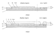
- FIG. 8 is a fifth schematic view illustrating a structure of an array substrate in an embodiment of the present invention.
- FIG. 9 is a sixth schematic view illustrating a structure of an array substrate in an embodiment of the present invention.
- the inventors found that the channel length of the conducting channel of a TFT in a conventional ADS type liquid crystal panel is larger due to the limitations of process factors, which not only reduces the value of the on-state current, but also indirectly limits the increase in the aperture ratio of a pixel; and in general, only if seven masking processes are used, the array substrate of the conventional ADS type liquid crystal panel can be manufactured, so the manufacturing difficulty and costs become higher, and the yield rate is lowered.
- Embodiments of the present invention provide an array substrate and its manufacturing method, and a display device; the array substrate reduces the channel length of the conducting channel of a thin film transistor unit, and meanwhile increases the aperture ratio of a pixel; and the manufacturing method can reduce the manufacturing difficulty of an array substrate, decrease the manufacturing costs, and increase the yield rate.
- the on-state current I on of the thin film transistor unit 2 of each pixel should be large enough and greater than 10 ⁇ 6 A generally.
- the channel length L is the thickness of the active layer 24 ; as long as the thickness of the active layer 24 is reduced, the channel length L can be decreased, to increase the on-state current I on , guarantee a high aperture ratio of the pixel in the meantime, and improve the display effect of a display device.
- the embodiment provides an array substrate, and the array substrate comprises a thin film transistor unit.
- the channel length of a conducting channel is the thickness of an active layer; as long as the thickness of the active layer is reduced, the channel length can be decreased, and thus to increase the on-state current, guarantee a high aperture ratio of a pixel in the meantime, and improve the display effect of a display device.
- the base substrate 1 can be made of a common transparent material such as glass, quartz or the like; the first gate electrode 21 or the source electrode 23 can have a thickness of from 100 nm to 500 nm, for example, can be made of a single-layer metal such as one of molybdenum, aluminum, tungsten, titanium and copper or any of their alloys, and can also be made of a multi-layer combination of the above-mentioned metals.
- the first gate electrode 21 and the source electrode 23 can further be made of a same material.
- the active layer 24 can be formed of a commonly used semiconductor material such as amorphous silicon, poly-silicon, indium gallium zinc oxide (IGZO) or the like, the thickness of which can be from 100 nm to 300 nm.
- the drain electrode 25 can comprise a common transparent conducting material such as tin indium oxide, indium zinc oxide or the like, the thickness of which can be from 50 nm to 500 nm.
- the display region further comprises a data line 3 and a gate line 4 that are provided on the base substrate and cross with each other vertically and horizontally. Generally a plurality of the data lines 3 and the gate lines 4 can be included; as illustrated in FIG.
- each data line 3 can comprise: a plurality of first data regions 31 disposed in a same layer as the gate lines 4 and insulated from the gate lines 4 and second data regions 32 provided on the first data regions 31 and connected to adjacent first data regions 31 , and the second data regions 32 and the gate lines 4 are partially overlapped with each other in an orthographic projection direction.
- a gate insulating layer 22 is disposed on the first data regions 31 and the gate line 4 ; first via holes 5 are each disposed in a portion of the gate insulating layer 22 corresponding to the first data region 31 ; and the second data region 32 is provided on the gate insulating layer 22 and electrically connected to the adjacent first data regions through the first via holes 5 .
- two first via holes 5 are provided, and respectively provided in portions of the adjacent two first data regions 31 close to the gate line 4 , symmetrical with respect to the gate line 4 .
- the gate line 4 and the data line 3 have to be insulated from each other. But as illustrated in FIG. 2 , in the display region, there's an overlapping portion between the gate line 4 and the data line 3 in the orthographic projection direction.
- the source electrode 23 and the first gate electrode 21 are disposed in a same layer; it's required that the gate line 4 and the first gate electrode 21 are disposed in a same layer and integrally formed without increasing the number of used masks, and it's also required that the data line 3 and the source electrode 23 are disposed in a same layer and integrally formed.
- the data line is divided into two kinds of regions: the first data regions 31 and the second data regions 32 .
- the first data regions 31 and the gate line 4 are disposed in a same layer, separated and insulated from each other.
- each thin film transistor unit 2 corresponds to one first data region 31 ;
- the second data regions 32 are provided on the gate insulating layer 22 ; and through the first via holes 5 that are disposed in the gate insulating layer 22 and correspond to the first data regions 31 , the first data regions 31 that are insulated from each other and correspond to two adjacent thin film transistor units 2 are electrically connected, to realize the normal transmission of data signals over the data line 3 .
- the second data region 32 and the drain electrode 25 can be disposed in a same layer and provided in a same pattern layer, namely, the second data regions 32 are formed at the time when the drain electrode 25 is formed through a patterning process.
- the second data region 32 can adopt a common transparent conducting material such as tin indium oxide, indium zinc oxide or the like, the thickness of which can be from 50 nm to 500 nm.
- the source electrode 23 , the first gate electrode 21 , the gate line 4 , the first data regions 31 of the data line 3 are disposed in a same layer, and the drain electrode 25 and the second data region 32 are provided in a same pattern layer.
- the first gate electrode 21 and the gate line 4 are integrally formed. In order to increase the control ability of the first gate electrode 21 for the conducting channel of the active layer 24 , the first gate electrode 21 is protruded from the gate line 4 .
- a first transparent conducting layer 6 is disposed on the thin film transistor unit 2 , and the first transparent conducting layer 6 and the drain electrode 25 can be integrally formed and electrically connected with each other.
- a passivation layer 7 is disposed on the drain electrode 25 and the first transparent conducting layer 6 .
- a passivation layer process can not only increase the resistance ability to a harsh environment for a display device, but also is helpful to improve the photoelectric performance parameters of a TFT.
- a second transparent conducting layer 8 is disposed on the passivation layer 7 , and at least a portion of the first transparent conducting layer 6 overlaps the second transparent conducting layer 8 .
- the first transparent conducting layer 6 and the drain electrode 25 are integrally formed, which means the connection between the first transparent conducting layer 6 and the drain electrode 25 , and here, the first transparent conducting layer 6 can be called as a pixel electrode; accordingly, the second transparent conducting layer 8 can be called as a common electrode.
- the first transparent conducting layer 6 and the second transparent conducting layer 8 cooperate to generate an electric field parallel to the base substrate 1 , and to drive the liquid crystal of an ADS type liquid crystal panel to rotate.
- the first transparent conducting layer 6 can be a plate-like electrode or a slit electrode
- the second transparent conducting layer 8 is a slit electrode
- the second transparent conducting layer 8 can be a common transparent conducting material such as tin indium oxide, indium zinc oxide or the like, and for example, the thickness can be from 50 nm to 500 nm.
- the drain electrode 25 can also be made of a single-layer metal such as one of molybdenum, aluminum, tungsten, titanium and copper or any of their alloys, or be made of a multi-layer combination of the above-mentioned metals.
- the first transparent conducting layer 6 is still made of the common transparent conducting material such as tin indium oxide, indium zinc oxide or the like.
- the first transparent conducting layer 6 can partially disposed on the drain electrode 25 , to realize the electrical connection between the two, as illustrated in FIG. 4 .
- a conventional technology generally uses a method of minimizing the process margin to the limit to manufacture a display with a narrow bezel, and one very important technology is the gate driver on array (GOA) technology.
- GOA gate driver on array
- a gate switch circuit is integrated on the array substrate of the display panel of a display device by using the GOA technology to realize the scan drive for the display panel, and thus the gate driving integrated circuit part can be omitted, the production costs can be reduced from both aspects of material cost and preparation process, and the display device can realize an attractive design in symmetrical sides and a narrow bezel.
- the array substrate can further comprise: a gate driver on array (GOA) unit 9 provided on the base substrate 1 , and the GOA unit 9 is provided in the GOA region of the array substrate.
- the GOA unit 9 comprises: a second gate electrode 91 provided on the base substrate 1 and a conducting leading wire 92 provided on the second gate electrode 91 .
- the first gate electrode 21 and the second gate electrode 91 of the thin film transistor unit 2 are disposed in a same layer, and the conducting leading wire 92 and the drain electrode 25 are provided in a same pattern layer.
- the second transparent conducting layer 8 in the GOA region is used for connecting a gate driver circuit and receiving the electrical signals from the gate driver circuit; after passing through the conducting leading wire 92 and the second gate electrode 91 , the electrical signals are transferred to the first gate electrode 21 of the thin film transistor unit 2 through the gate line on the array substrate to drive the thin film transistor unit 2 to work.
- a second via hole 10 is disposed in a portion of the passivation layer 7 corresponding to the conducting leading wire 92 , and the second transparent conducting layer 8 can be electrically connected to the conducting leading wire 92 through the second via hole 10 , and thus realize the connection to the gate line 4 and first gate electrode 21 through the second gate electrode 91 .
- Such a connection way needs a simple processing technology and has stable connection effect.
- the gate line 4 and the first gate electrode 21 can be disposed in a same layer and be integrally formed.
- An embodiment of the present invention further provides a display device, which comprises any of the above-mentioned array substrates.
- the display device can be any product or component that has a display function, such as a liquid crystal panel, an electronic paper, an organic light-emitting diode (OELD) display panel, a mobile phone, a tablet computer, a television, a display, a laptop computer, a digital photo-frame, a navigating instrument or the like.
- a display function such as a liquid crystal panel, an electronic paper, an organic light-emitting diode (OELD) display panel, a mobile phone, a tablet computer, a television, a display, a laptop computer, a digital photo-frame, a navigating instrument or the like.
- OELD organic light-emitting diode
- the embodiment of the present invention provides a manufacturing method of an array substrate as illustrated in FIG. 1 , and the method comprises the following process of forming a thin film transistor unit:
- Step S 11 a pattern that comprises a first gate electrode and a source electrode is formed on a base substrate, and the first gate electrode and the source electrode is formed in a same layer.
- Step S 12 a pattern that comprises a gate insulating layer is formed on the pattern formed in step S 11 , and a pattern that comprises an active layer is formed on the source electrode.
- the gate insulating layer is formed on the first gate electrode, and between the patterns of the first gate electrode and the source electrode.
- Step S 13 a pattern that comprises a drain electrode is formed on the active layer formed in the step S 12 .
- the manufacturing method of an array substrate provided by the embodiment can further comprise the following process of forming a data line and a gate line: in the step S 11 , a pattern that comprises the first gate electrode, the source electrode, the gate line, the first data regions of the data line is formed in a same layer on the base substrate; in the step S 12 , first via holes are formed in the gate insulating layer corresponding to the first data region; and in the step S 13 , a pattern that comprises the drain electrode and a second data region of the data line is formed in a same layer, and the second data region electrically connects an adjacent first data regions through the first via holes.
- a pattern that comprises the drain electrode and a first transparent conducting layer can be formed in a same layer in the step S 13 .
- the embodiment can further comprise:
- Step S 14 a pattern that comprises a passivation layer and a pattern that comprises a second transparent conducting layer are sequentially formed on the pattern formed in the step S 13 .
- the manufacturing method of an array substrate provided by the embodiment can further comprise a process of forming a gate driver on array unit, which comprises: in the step S 11 , a pattern that comprises the first gate electrode, the source electrode, the gate line, the first data regions of the data line, and the second gate electrode is formed in a same layer on the base substrate; in the step S 13 , a pattern that comprises the drain electrode, the first transparent conducting layer, the second data region of the data line, and the conducting leading wire is formed in a same layer.
- Different structures disposed in a same layer can be formed in a same patterning process, and can also be formed in a plurality of patterning processes respectively, and there are no limitations in the embodiment.
- a second via hole is disposed in a portion of the passivation layer corresponding to the conducting leading wire, and the second transparent conducting layer electrically connects the conducting leading wire through the second via hole.
- the source electrode, the first gate electrode and the gate line of the array substrate manufactured in the above-mentioned manufacturing method of an array substrate are formed in a same layer, and can be formed together in a same patterning process; similarly, the first gate electrode and the first data regions are formed in a same layer.
- the first transparent conducting layer 6 can be a plate-like electrode or a slit electrode
- the second transparent conducting layer 8 is a slit electrode
- Step S 101 a metal thin film and a semiconductor thin film are sequentially formed on a base substrate; a pattern that comprises the first gate electrode of the thin film transistor unit, the source electrode and the active layer, the gate line, the first data regions of the data line and the second gate electrode of the gate driver on array unit is etched and formed through a first masking process.
- a metal thin film 11 is formed on the base substrate 1 by using a magnetron sputtering, a thermal evaporation or the like method, followed by depositing a semiconductor thin film 12 through a plasma enhanced chemical vapor deposition (PECVD) method.
- PECVD plasma enhanced chemical vapor deposition
- the gate line 4 and the first gate electrode 21 , the second gate electrode 91 are integrally formed, the first data regions 31 and the source electrode 23 are integrally formed, and this not only strengthens the connection between them, but also reduces processes, and in the meantime, simplifies the layer structure of the array substrate.
- photoresist 13 is coated on the semiconductor thin film 12 ; a two-tone mask, for example, a half-tone or a gray-tone mask is used to perform an exposure, so that the photoresist forms a complete-exposed region, an unexposed region and a partially-exposed region; a pattern of the photoresist 13 is obtained after development for the photoresist during the developing process, as illustrated in FIG. 5 a .
- a two-tone mask for example, a half-tone or a gray-tone mask is used to perform an exposure, so that the photoresist forms a complete-exposed region, an unexposed region and a partially-exposed region
- a pattern of the photoresist 13 is obtained after development for the photoresist during the developing process, as illustrated in FIG. 5 a .
- the semiconductor thin film 12 and the metal thin film 11 that correspond to the complete-exposed region are etched by using the pattern of the photoresist 13 through an etching process, to form a pattern that comprises the source electrode 23 , the first gate electrode 21 , the first data regions 31 (not shown in the drawing), the gate line 4 (not shown in the drawing) and the second gate electrode 92 ; the photoresist 13 in the partially-exposed region are removed through an ashing process, to expose the semiconductor thin film 12 that corresponds to the partially-exposed region; and the exposed semiconductor thin film 12 is completely etched through an etching process to form a pattern that comprises the active layer 24 of thin film transistor unit 2 , as illustrated in FIG. 5 b ; and finally, the rest photoresist 13 is stripped to form the array substrate illustrated in FIG. 6 .
- the material of the base substrate 1 is generally glass or quartz;
- the metal thin film 11 can be made of a single-layer metal such as one of molybdenum, aluminum, tungsten, titanium and copper or any of their alloys, and can also be made of a multi-layer combination of the above-mentioned metals, with a thickness of from 50 nm to 500 nm;
- the semiconductor thin film 12 can be formed of a semiconductor material such as amorphous silicon, poly-silicon, indium gallium zinc oxide or the like, with a thickness of from 100 nm to 300 nm.
- Step S 102 a first insulating thin film is formed, a pattern that comprises the gate insulating layer is etched and formed through a second masking process, and the first via holes are formed in the gate insulating layer corresponding to the first data regions.
- a layer of the first insulating thin film is deposited by using a PECVD method; in the second masking process, patterns of the gate insulating layer 22 , exposing the active layer 24 and of the second gate electrode 91 of the GOA unit 9 , are formed by using a common mask through a patterning process, as illustrated in FIG. 7 .
- the gate insulating layer 22 is provided on the first gate electrode 21 , and the gate insulating layer 22 (this part of the gate insulating layer 22 is provided on the base substrate 1 ) is provided between the first gate electrode 21 and the source electrode 23 .
- both the gate line 4 and the first data regions 31 are covered with the gate insulating layer 22 thereon, and in order to guarantee the insulation between the gate line 4 and the data line 3 , the gate insulating layer 22 (this part of the gate insulating layer 22 is provided on the base substrate 1 ) is provided between the gate line 4 and the first data regions 31 .
- the formed pattern of the gate insulating layer 22 further comprises first via holes 5 corresponding to the first data regions 31 .
- the gate insulating layer 22 comprises silicon oxide as an insulating material, preferably; in the meantime, it can also use silicon nitride, hafnium oxide or the like insulating material, and can also be of a multi-layer combination of the above-mentioned insulating materials, with a thickness of from 100 nm to 300 nm.
- Step S 103 a first transparent thin film is formed, a pattern that comprises the drain electrode of the thin film transistor unit and the first transparent conducting layer, the second data region of the data line and the conducting leading wire of a GOA is etched and formed through a third masking process, and the second data region electrically connects the adjacent first data regions through the first via holes.
- a layer of the first transparent thin film is formed by using a magnetron sputtering, a thermal evaporation or the like method, and the first transparent thin film can adopt tin indium oxide, indium zinc oxide or the similar material, with a thickness of from 50 nm to 500 nm; a pattern that comprises the drain electrode 25 and the first transparent conducting layer 6 is formed using a common mask through a patterning process in the display region, and the first transparent conducting layer 6 and the drain electrode 25 are integrally formed, which increases the transmission reliability of signals between the drain electrode 25 and the first transparent conducting layer 6 .
- a pattern that comprises the second data region 32 can be further formed, and the second data region 32 can electrically connect the adjacent first data regions 31 through the first via holes 5 in the gate insulating layer 22 ; two first data regions 31 that are insulated from each other can be connected to form a data line 3 , as illustrated in FIG. 3 .
- a pattern that comprises the conducting leading wire 92 in the GOA region can further be formed using the first transparent thin film, to form the structure of the array substrate illustrated in FIG. 8 .
- Step S 104 a second insulating thin film is formed, a pattern that comprises a passivation layer is etched and formed through a fourth masking process, and a second via hole is disposed in a portion of the passivation layer corresponding to the conducting leading wire.
- a layer of the second insulating thin film is deposited by using a PECVD method, and similarly, the second insulating thin film can adopt a same material as the gate insulating layer 22 , with a thickness of from 100 nm to 300 nm.
- the second insulating thin film is etched by using a common mask through a patterning process, to form a pattern that comprises the passivation layer 7 , and the second via hole 10 is disposed in a portion of the passivation layer 7 corresponding to the conducting leading wire 92 , as illustrated in FIG. 9 .
- Step S 105 a second transparent conducting thin film is formed, a pattern that comprises the second transparent conducting layer is etched and formed through a fifth masking process, and the second transparent conducting layer and the conducting leading wire are electrically connected through the second via hole.
- a layer of the second transparent conducting thin film is formed by using a magnetron sputtering, a thermal evaporation or the like method, and the second transparent conducting thin film can adopt tin indium oxide, indium zinc oxide or the like material, with a thickness of from 50 nm to 500 nm.
- a pattern that comprises the second transparent conducting layer 8 is formed by using a common mask through a patterning process, and the electrical connection between the second transparent conducting layer 8 and the conducting leading wire 92 is realized through the second via hole 10 .
- the array substrate illustrated in FIG. 1 can be obtained.
- the second transparent conducting layer 8 is a slit electrode.
- the second transparent conducting layer 8 in the GOA region is used for connecting a gate driver circuit and receiving the electrical signals from the gate driver circuit, and the electrical signals is transferred to the thin film transistor unit 2 of the array substrate after passing through the conducting leading wire 92 and the gate line 4 , to drive the thin film transistor unit 2 to work.
- the above-mentioned example use five masking processes only to realize the manufacture of an array substrate, and as compared with a conventional technology, can reduce two masking processes, decrease the manufacturing difficulty and manufacturing costs, and increase the yield rate of the manufactured array substrate.
- the drain electrode 25 and the first transparent conducting layer 6 are integrally formed using the first transparent thin film in a same patterning process.
- the metal can be of a single-layer metal such as one of molybdenum, aluminum, tungsten, titanium, copper or any of their alloys, and can also be of a multi-layer combination of the above-mentioned metals.
- the first transparent conducting layer 6 and the drain electrode 25 are unable to be integrally fainted with a metal material similarly, and thus two patterning processes are required to manufacture and form the drain electrode 25 and the first transparent conducting layer 6 that is disposed in a same layer as the drain electrode 25 and connects the same, which is equivalent to the realization of manufacture of the array substrate with six masking processes.
- the first transparent conducting layer 6 can partially disposed on the drain electrode 25 , namely, partially overlap on the drain electrode 25 , as illustrated in FIG. 4 .
- the patterning process may only comprise a photolithography process, or comprise the photolithography process and an etching step, and may also comprise printing, ink-jet or other similar processes used for faulting a predetermined pattern;
- the photolithography process refers to a process including film-forming, exposing, developing, and the like process and using photoresist, a mask, an exposure machine and the like to form a pattern.
- the corresponding patterning process can be chosen according to the formed structure in the embodiments of the present invention.
- the five or six masking processes denoted in the embodiments of the present invention refer to that five or six masks are used; the photolithography process, etching step or the other processes may also be used; the term masking process is used for comparing with the conventional seven mask processes, but it does not represent that the process of the embodiments of the present invention only comprises this process using a mask; and the rest processes can be selected according to the need.
- the common mask in the embodiments of the present invention is called compared with a two-tone mask, and when a single-tone mask or a common mask is used, it's required to make corresponding modifications according to the different formed patterns.
Landscapes
- Liquid Crystal (AREA)
- Thin Film Transistor (AREA)
- Devices For Indicating Variable Information By Combining Individual Elements (AREA)
- Chemical & Material Sciences (AREA)
- Crystallography & Structural Chemistry (AREA)
Applications Claiming Priority (4)
| Application Number | Priority Date | Filing Date | Title |
|---|---|---|---|
| CN201310314225.XA CN103413812B (zh) | 2013-07-24 | 2013-07-24 | 阵列基板及其制备方法、显示装置 |
| CN201310314225.X | 2013-07-24 | ||
| CN201310314225 | 2013-07-24 | ||
| PCT/CN2013/086376 WO2015010384A1 (fr) | 2013-07-24 | 2013-10-31 | Substrat de réseau, son procédé de préparation, et dispositif d'affichage |
Publications (2)
| Publication Number | Publication Date |
|---|---|
| US20160247821A1 US20160247821A1 (en) | 2016-08-25 |
| US9613986B2 true US9613986B2 (en) | 2017-04-04 |
Family
ID=49606810
Family Applications (1)
| Application Number | Title | Priority Date | Filing Date |
|---|---|---|---|
| US14/388,182 Expired - Fee Related US9613986B2 (en) | 2013-07-24 | 2013-10-31 | Array substrate and its manufacturing method, display device |
Country Status (3)
| Country | Link |
|---|---|
| US (1) | US9613986B2 (fr) |
| CN (1) | CN103413812B (fr) |
| WO (1) | WO2015010384A1 (fr) |
Cited By (2)
| Publication number | Priority date | Publication date | Assignee | Title |
|---|---|---|---|---|
| US20170017130A1 (en) * | 2014-12-24 | 2017-01-19 | Boe Technology Group Co., Ltd. | Goa circuit module, method for testing the same, display panel and display apparatus |
| US10224406B2 (en) * | 2016-08-31 | 2019-03-05 | Shenzhen China Star Optoelectronics Technology Co., Ltd. | Array substrate including vertical TFT, and manufacturing method thereof |
Families Citing this family (13)
| Publication number | Priority date | Publication date | Assignee | Title |
|---|---|---|---|---|
| CN104090442A (zh) * | 2014-07-15 | 2014-10-08 | 京东方科技集团股份有限公司 | 阵列基板、液晶显示装置和阵列基板的制作方法 |
| CN104465669A (zh) * | 2014-12-04 | 2015-03-25 | 京东方科技集团股份有限公司 | 阵列基板及其制作方法、显示装置 |
| CN104617102B (zh) * | 2014-12-31 | 2017-11-03 | 深圳市华星光电技术有限公司 | 阵列基板及阵列基板制造方法 |
| CN104810375B (zh) * | 2015-04-28 | 2018-09-04 | 合肥鑫晟光电科技有限公司 | 一种阵列基板及其制作方法和一种显示装置 |
| CN204964955U (zh) * | 2015-07-28 | 2016-01-13 | 合肥鑫晟光电科技有限公司 | 电连接结构、阵列基板和显示装置 |
| CN105093748A (zh) * | 2015-08-13 | 2015-11-25 | 武汉华星光电技术有限公司 | 液晶面板及其阵列基板 |
| CN105629614A (zh) | 2016-03-29 | 2016-06-01 | 京东方科技集团股份有限公司 | 阵列基板及其制造方法、显示面板和显示装置 |
| CN106684037B (zh) * | 2017-03-22 | 2019-09-24 | 深圳市华星光电半导体显示技术有限公司 | 优化4m制程的tft阵列制备方法 |
| CN113724667B (zh) * | 2020-04-10 | 2023-04-07 | 京东方科技集团股份有限公司 | 显示基板及其制作方法、显示装置 |
| CN111584523B (zh) * | 2020-05-25 | 2023-09-12 | 成都京东方显示科技有限公司 | 阵列基板、显示面板以及阵列基板的制作方法 |
| CN111584520B (zh) * | 2020-05-25 | 2023-09-12 | 成都京东方显示科技有限公司 | 阵列基板、显示面板以及阵列基板的制作方法 |
| CN115398523B (zh) | 2021-01-27 | 2025-08-05 | 京东方科技集团股份有限公司 | 像素驱动电路及其驱动方法、显示基板、显示装置 |
| CN114743994B (zh) * | 2022-05-11 | 2025-10-24 | 武汉华星光电技术有限公司 | 阵列基板、显示面板及显示终端 |
Citations (7)
| Publication number | Priority date | Publication date | Assignee | Title |
|---|---|---|---|---|
| US6320221B1 (en) | 1998-12-30 | 2001-11-20 | Hyundai Electronics Industries Co., Ltd. | TFT-LCD having a vertical thin film transistor |
| JP2007043137A (ja) | 2005-07-05 | 2007-02-15 | Advanced Lcd Technologies Development Center Co Ltd | nチャネル型薄膜トランジスタ、nチャネル型薄膜トランジスタの製造方法および表示装置 |
| JP2010045240A (ja) | 2008-08-14 | 2010-02-25 | Citizen Watch Co Ltd | 縦型mosfet |
| US20110101338A1 (en) * | 2009-10-30 | 2011-05-05 | Semiconductor Energy Laboratory Co., Ltd. | Non-linear element, display device including non-linear element, and electronic device including display device |
| CN103018991A (zh) | 2012-12-24 | 2013-04-03 | 京东方科技集团股份有限公司 | 一种阵列基板及其制造方法、显示装置 |
| CN103309105A (zh) | 2013-07-05 | 2013-09-18 | 北京京东方光电科技有限公司 | 阵列基板及其制备方法、显示装置 |
| CN203455564U (zh) | 2013-07-24 | 2014-02-26 | 北京京东方光电科技有限公司 | 阵列基板及显示装置 |
Family Cites Families (1)
| Publication number | Priority date | Publication date | Assignee | Title |
|---|---|---|---|---|
| CN202601619U (zh) * | 2012-01-09 | 2012-12-12 | 京东方科技集团股份有限公司 | 一种薄膜晶体管、阵列基板和显示器 |
-
2013
- 2013-07-24 CN CN201310314225.XA patent/CN103413812B/zh not_active Expired - Fee Related
- 2013-10-31 US US14/388,182 patent/US9613986B2/en not_active Expired - Fee Related
- 2013-10-31 WO PCT/CN2013/086376 patent/WO2015010384A1/fr not_active Ceased
Patent Citations (8)
| Publication number | Priority date | Publication date | Assignee | Title |
|---|---|---|---|---|
| US6320221B1 (en) | 1998-12-30 | 2001-11-20 | Hyundai Electronics Industries Co., Ltd. | TFT-LCD having a vertical thin film transistor |
| JP2007043137A (ja) | 2005-07-05 | 2007-02-15 | Advanced Lcd Technologies Development Center Co Ltd | nチャネル型薄膜トランジスタ、nチャネル型薄膜トランジスタの製造方法および表示装置 |
| JP2010045240A (ja) | 2008-08-14 | 2010-02-25 | Citizen Watch Co Ltd | 縦型mosfet |
| US20110101338A1 (en) * | 2009-10-30 | 2011-05-05 | Semiconductor Energy Laboratory Co., Ltd. | Non-linear element, display device including non-linear element, and electronic device including display device |
| CN103018991A (zh) | 2012-12-24 | 2013-04-03 | 京东方科技集团股份有限公司 | 一种阵列基板及其制造方法、显示装置 |
| US20140175446A1 (en) | 2012-12-24 | 2014-06-26 | Boe Technology Group Co., Ltd. | Array substrate, method for manufacturing the same, and display device |
| CN103309105A (zh) | 2013-07-05 | 2013-09-18 | 北京京东方光电科技有限公司 | 阵列基板及其制备方法、显示装置 |
| CN203455564U (zh) | 2013-07-24 | 2014-02-26 | 北京京东方光电科技有限公司 | 阵列基板及显示装置 |
Non-Patent Citations (3)
| Title |
|---|
| First Chinese Office Action Appln. No. 201310314225.X; Dated Jun. 8, 2015. |
| International Preliminary Report on Patentability Appln. No. PCT/CN2013/086376; Dated Jan. 26, 2016. |
| International Search Report Appln. No. PCt/CN2013/086376; Dated Apr. 16, 2014. |
Cited By (3)
| Publication number | Priority date | Publication date | Assignee | Title |
|---|---|---|---|---|
| US20170017130A1 (en) * | 2014-12-24 | 2017-01-19 | Boe Technology Group Co., Ltd. | Goa circuit module, method for testing the same, display panel and display apparatus |
| US9983450B2 (en) * | 2014-12-24 | 2018-05-29 | Boe Technology Group Co., Ltd. | GOA circuit module, method for testing the same, display panel and display apparatus |
| US10224406B2 (en) * | 2016-08-31 | 2019-03-05 | Shenzhen China Star Optoelectronics Technology Co., Ltd. | Array substrate including vertical TFT, and manufacturing method thereof |
Also Published As
| Publication number | Publication date |
|---|---|
| WO2015010384A1 (fr) | 2015-01-29 |
| US20160247821A1 (en) | 2016-08-25 |
| CN103413812B (zh) | 2016-08-17 |
| CN103413812A (zh) | 2013-11-27 |
Similar Documents
| Publication | Publication Date | Title |
|---|---|---|
| US9613986B2 (en) | Array substrate and its manufacturing method, display device | |
| US11049975B2 (en) | Dual-gate thin film transistor, manufacturing method thereof, array substrate and display device | |
| CN105097947B (zh) | 薄膜晶体管阵列基板及其制造方法 | |
| CN103456742B (zh) | 一种阵列基板及其制作方法、显示装置 | |
| CN103383945B (zh) | 一种阵列基板、显示装置及阵列基板的制造方法 | |
| US9881942B2 (en) | Array substrate, manufacturing method thereof and display device | |
| CN102881688B (zh) | 一种阵列基板、显示面板及阵列基板的制造方法 | |
| WO2018099052A1 (fr) | Procédé de fabrication de substrat de réseau, substrat de réseau et appareil d'affichage | |
| US20150214253A1 (en) | Array substrate, manufacturing method thereof and display device | |
| US9711544B2 (en) | Thin film transistor and manufacturing method thereof, array substrate and manufacturing method thereof, display device | |
| US9484364B2 (en) | Array substrate and method for manufacturing the same, display device | |
| US8895334B2 (en) | Thin film transistor array substrate and method for manufacturing the same and electronic device | |
| US9761617B2 (en) | Method for manufacturing array substrate, array substrate and display device | |
| CN106783737B (zh) | 阵列基板及其制造方法、显示面板、显示装置 | |
| US20160254275A1 (en) | Array substrate and manufacturing method thereof, and display device | |
| US20140048826A1 (en) | Array substrate and its manufacturing method | |
| US20160181278A1 (en) | Array substrate, method for manufacturing the same, and display device | |
| WO2017140058A1 (fr) | Substrat de matrice, son procédé de fabrication, écran d'affichage et appareil d'affichage | |
| US9490270B2 (en) | Array substrate and manufacturing method thereof, and display device including the array substrate | |
| CN102709328B (zh) | 一种阵列基板、其制造方法、显示面板及显示装置 | |
| WO2016000363A1 (fr) | Substrat de matrice de transistors à couches minces au polysilicium basse température et son procédé de fabrication, et dispositif d'affichage | |
| CN203445120U (zh) | 一种阵列基板及显示装置 | |
| CN204029807U (zh) | 一种低温多晶硅薄膜晶体管阵列基板、显示装置 | |
| KR101338739B1 (ko) | 액정 표시 장치용 박막 트랜지스터 기판 및 이의 제조 방법 |
Legal Events
| Date | Code | Title | Description |
|---|---|---|---|
| AS | Assignment |
Owner name: BEIJING BOE OPTOELECTRONICS TECHNOLOGY CO., LTD., Free format text: ASSIGNMENT OF ASSIGNORS INTEREST;ASSIGNORS:LI, JING;LIU, FANG;REEL/FRAME:033824/0973 Effective date: 20140912 Owner name: BOE TECHNOLOGY GROUP CO., LTD., CHINA Free format text: ASSIGNMENT OF ASSIGNORS INTEREST;ASSIGNORS:LI, JING;LIU, FANG;REEL/FRAME:033824/0973 Effective date: 20140912 |
|
| STCF | Information on status: patent grant |
Free format text: PATENTED CASE |
|
| MAFP | Maintenance fee payment |
Free format text: PAYMENT OF MAINTENANCE FEE, 4TH YEAR, LARGE ENTITY (ORIGINAL EVENT CODE: M1551); ENTITY STATUS OF PATENT OWNER: LARGE ENTITY Year of fee payment: 4 |
|
| FEPP | Fee payment procedure |
Free format text: MAINTENANCE FEE REMINDER MAILED (ORIGINAL EVENT CODE: REM.); ENTITY STATUS OF PATENT OWNER: LARGE ENTITY |
|
| LAPS | Lapse for failure to pay maintenance fees |
Free format text: PATENT EXPIRED FOR FAILURE TO PAY MAINTENANCE FEES (ORIGINAL EVENT CODE: EXP.); ENTITY STATUS OF PATENT OWNER: LARGE ENTITY |
|
| STCH | Information on status: patent discontinuation |
Free format text: PATENT EXPIRED DUE TO NONPAYMENT OF MAINTENANCE FEES UNDER 37 CFR 1.362 |
|
| FP | Lapsed due to failure to pay maintenance fee |
Effective date: 20250404 |