US9722121B2 - Nanostructured units formed inside a silicon material and the manufacturing process to perform them therein - Google Patents
Nanostructured units formed inside a silicon material and the manufacturing process to perform them therein Download PDFInfo
- Publication number
- US9722121B2 US9722121B2 US14/890,603 US201414890603A US9722121B2 US 9722121 B2 US9722121 B2 US 9722121B2 US 201414890603 A US201414890603 A US 201414890603A US 9722121 B2 US9722121 B2 US 9722121B2
- Authority
- US
- United States
- Prior art keywords
- silicon
- crystalline
- elementary
- set forth
- crystalline silicon
- Prior art date
- Legal status (The legal status is an assumption and is not a legal conclusion. Google has not performed a legal analysis and makes no representation as to the accuracy of the status listed.)
- Active
Links
- 238000004519 manufacturing process Methods 0.000 title abstract description 22
- 239000002210 silicon-based material Substances 0.000 title abstract description 4
- XUIMIQQOPSSXEZ-UHFFFAOYSA-N Silicon Chemical compound [Si] XUIMIQQOPSSXEZ-UHFFFAOYSA-N 0.000 claims abstract description 142
- 229910052710 silicon Inorganic materials 0.000 claims abstract description 107
- 239000010703 silicon Substances 0.000 claims abstract description 105
- 238000006243 chemical reaction Methods 0.000 claims abstract description 36
- 239000004065 semiconductor Substances 0.000 claims abstract description 25
- 238000005468 ion implantation Methods 0.000 claims abstract description 20
- 238000007669 thermal treatment Methods 0.000 claims abstract description 12
- 229910021419 crystalline silicon Inorganic materials 0.000 claims description 136
- 229910021417 amorphous silicon Inorganic materials 0.000 claims description 44
- 238000000034 method Methods 0.000 claims description 34
- 150000002500 ions Chemical class 0.000 claims description 24
- 238000002513 implantation Methods 0.000 claims description 20
- 230000007704 transition Effects 0.000 claims description 19
- 238000000137 annealing Methods 0.000 claims description 15
- 230000003750 conditioning effect Effects 0.000 claims description 15
- 238000010521 absorption reaction Methods 0.000 claims description 11
- 239000002784 hot electron Substances 0.000 claims description 11
- 238000005286 illumination Methods 0.000 claims description 11
- 230000005684 electric field Effects 0.000 claims description 8
- 230000008569 process Effects 0.000 claims description 7
- BHEPBYXIRTUNPN-UHFFFAOYSA-N hydridophosphorus(.) (triplet) Chemical compound [PH] BHEPBYXIRTUNPN-UHFFFAOYSA-N 0.000 claims description 6
- 238000010884 ion-beam technique Methods 0.000 claims description 6
- 238000010894 electron beam technology Methods 0.000 claims description 5
- ZOXJGFHDIHLPTG-UHFFFAOYSA-N Boron Chemical compound [B] ZOXJGFHDIHLPTG-UHFFFAOYSA-N 0.000 claims description 3
- 229910052796 boron Inorganic materials 0.000 claims description 3
- 238000011161 development Methods 0.000 claims description 3
- -1 phosphorous ions Chemical class 0.000 claims 4
- 230000003213 activating effect Effects 0.000 claims 2
- 239000000463 material Substances 0.000 abstract description 36
- 230000009466 transformation Effects 0.000 abstract description 22
- 238000001228 spectrum Methods 0.000 abstract description 14
- 238000000844 transformation Methods 0.000 abstract description 11
- 238000006073 displacement reaction Methods 0.000 abstract description 5
- 239000013078 crystal Substances 0.000 abstract description 4
- 230000005611 electricity Effects 0.000 abstract description 4
- 238000000151 deposition Methods 0.000 abstract description 3
- 230000008021 deposition Effects 0.000 abstract description 3
- 230000000704 physical effect Effects 0.000 abstract description 3
- 238000012545 processing Methods 0.000 description 25
- 230000007246 mechanism Effects 0.000 description 15
- 238000009826 distribution Methods 0.000 description 14
- 230000007547 defect Effects 0.000 description 12
- 230000001143 conditioned effect Effects 0.000 description 11
- 238000005280 amorphization Methods 0.000 description 9
- 239000012535 impurity Substances 0.000 description 9
- 230000003993 interaction Effects 0.000 description 9
- 230000000694 effects Effects 0.000 description 8
- 238000000605 extraction Methods 0.000 description 8
- 239000002052 molecular layer Substances 0.000 description 8
- 239000002159 nanocrystal Substances 0.000 description 8
- 238000009792 diffusion process Methods 0.000 description 6
- 238000001953 recrystallisation Methods 0.000 description 6
- 239000000969 carrier Substances 0.000 description 5
- 230000008929 regeneration Effects 0.000 description 5
- 238000011069 regeneration method Methods 0.000 description 5
- 239000007787 solid Substances 0.000 description 5
- VYPSYNLAJGMNEJ-UHFFFAOYSA-N Silicium dioxide Chemical compound O=[Si]=O VYPSYNLAJGMNEJ-UHFFFAOYSA-N 0.000 description 4
- 238000000407 epitaxy Methods 0.000 description 4
- 238000003780 insertion Methods 0.000 description 4
- 230000037431 insertion Effects 0.000 description 4
- 230000005693 optoelectronics Effects 0.000 description 4
- 238000007493 shaping process Methods 0.000 description 4
- 238000009825 accumulation Methods 0.000 description 3
- 230000004913 activation Effects 0.000 description 3
- 230000000295 complement effect Effects 0.000 description 3
- 238000013461 design Methods 0.000 description 3
- 238000005516 engineering process Methods 0.000 description 3
- 230000006872 improvement Effects 0.000 description 3
- 238000002347 injection Methods 0.000 description 3
- 239000007924 injection Substances 0.000 description 3
- 230000004807 localization Effects 0.000 description 3
- 239000011159 matrix material Substances 0.000 description 3
- 230000002035 prolonged effect Effects 0.000 description 3
- 230000005855 radiation Effects 0.000 description 3
- 230000006798 recombination Effects 0.000 description 3
- 238000005215 recombination Methods 0.000 description 3
- 238000004435 EPR spectroscopy Methods 0.000 description 2
- 238000003917 TEM image Methods 0.000 description 2
- 239000012237 artificial material Substances 0.000 description 2
- 238000012512 characterization method Methods 0.000 description 2
- 229910052681 coesite Inorganic materials 0.000 description 2
- 229910052906 cristobalite Inorganic materials 0.000 description 2
- 230000006378 damage Effects 0.000 description 2
- 230000014509 gene expression Effects 0.000 description 2
- 238000010438 heat treatment Methods 0.000 description 2
- 238000001465 metallisation Methods 0.000 description 2
- 238000012986 modification Methods 0.000 description 2
- 230000004048 modification Effects 0.000 description 2
- 239000002086 nanomaterial Substances 0.000 description 2
- 238000002161 passivation Methods 0.000 description 2
- 230000008521 reorganization Effects 0.000 description 2
- 238000000926 separation method Methods 0.000 description 2
- 239000000377 silicon dioxide Substances 0.000 description 2
- 229910052682 stishovite Inorganic materials 0.000 description 2
- 230000002123 temporal effect Effects 0.000 description 2
- 230000007723 transport mechanism Effects 0.000 description 2
- 229910052905 tridymite Inorganic materials 0.000 description 2
- 229910001218 Gallium arsenide Inorganic materials 0.000 description 1
- 230000001133 acceleration Effects 0.000 description 1
- 230000009471 action Effects 0.000 description 1
- 230000006978 adaptation Effects 0.000 description 1
- 230000004888 barrier function Effects 0.000 description 1
- JJWKPURADFRFRB-UHFFFAOYSA-N carbonyl sulfide Chemical compound O=C=S JJWKPURADFRFRB-UHFFFAOYSA-N 0.000 description 1
- 230000008859 change Effects 0.000 description 1
- 239000011248 coating agent Substances 0.000 description 1
- 238000000576 coating method Methods 0.000 description 1
- 230000002301 combined effect Effects 0.000 description 1
- 239000002178 crystalline material Substances 0.000 description 1
- 230000003247 decreasing effect Effects 0.000 description 1
- 230000018109 developmental process Effects 0.000 description 1
- 238000010586 diagram Methods 0.000 description 1
- 238000007599 discharging Methods 0.000 description 1
- 238000004090 dissolution Methods 0.000 description 1
- 230000007613 environmental effect Effects 0.000 description 1
- 238000005530 etching Methods 0.000 description 1
- 239000003574 free electron Substances 0.000 description 1
- 238000009499 grossing Methods 0.000 description 1
- 238000000265 homogenisation Methods 0.000 description 1
- 238000010348 incorporation Methods 0.000 description 1
- 230000031700 light absorption Effects 0.000 description 1
- 238000013507 mapping Methods 0.000 description 1
- 230000000873 masking effect Effects 0.000 description 1
- 239000012528 membrane Substances 0.000 description 1
- 239000002105 nanoparticle Substances 0.000 description 1
- 230000003287 optical effect Effects 0.000 description 1
- 230000008520 organization Effects 0.000 description 1
- 230000001151 other effect Effects 0.000 description 1
- 230000035515 penetration Effects 0.000 description 1
- 230000010399 physical interaction Effects 0.000 description 1
- 238000002203 pretreatment Methods 0.000 description 1
- 238000004064 recycling Methods 0.000 description 1
- 238000002310 reflectometry Methods 0.000 description 1
- 238000011160 research Methods 0.000 description 1
- 238000012216 screening Methods 0.000 description 1
- 230000003595 spectral effect Effects 0.000 description 1
- 230000007847 structural defect Effects 0.000 description 1
- 230000001988 toxicity Effects 0.000 description 1
- 231100000419 toxicity Toxicity 0.000 description 1
- 238000011282 treatment Methods 0.000 description 1
- 230000001960 triggered effect Effects 0.000 description 1
Images


Classifications
-
- H—ELECTRICITY
- H10—SEMICONDUCTOR DEVICES; ELECTRIC SOLID-STATE DEVICES NOT OTHERWISE PROVIDED FOR
- H10F—INORGANIC SEMICONDUCTOR DEVICES SENSITIVE TO INFRARED RADIATION, LIGHT, ELECTROMAGNETIC RADIATION OF SHORTER WAVELENGTH OR CORPUSCULAR RADIATION
- H10F10/00—Individual photovoltaic cells, e.g. solar cells
- H10F10/10—Individual photovoltaic cells, e.g. solar cells having potential barriers
- H10F10/13—Photovoltaic cells having absorbing layers comprising graded bandgaps
-
- H01L31/065—
-
- H01L31/0288—
-
- H01L31/0352—
-
- H01L31/035236—
-
- H01L31/036—
-
- H01L31/03682—
-
- H01L31/03762—
-
- H01L31/068—
-
- H01L31/1804—
-
- H01L31/1864—
-
- H01L31/202—
-
- H—ELECTRICITY
- H10—SEMICONDUCTOR DEVICES; ELECTRIC SOLID-STATE DEVICES NOT OTHERWISE PROVIDED FOR
- H10F—INORGANIC SEMICONDUCTOR DEVICES SENSITIVE TO INFRARED RADIATION, LIGHT, ELECTROMAGNETIC RADIATION OF SHORTER WAVELENGTH OR CORPUSCULAR RADIATION
- H10F10/00—Individual photovoltaic cells, e.g. solar cells
- H10F10/10—Individual photovoltaic cells, e.g. solar cells having potential barriers
- H10F10/14—Photovoltaic cells having only PN homojunction potential barriers
-
- H—ELECTRICITY
- H10—SEMICONDUCTOR DEVICES; ELECTRIC SOLID-STATE DEVICES NOT OTHERWISE PROVIDED FOR
- H10F—INORGANIC SEMICONDUCTOR DEVICES SENSITIVE TO INFRARED RADIATION, LIGHT, ELECTROMAGNETIC RADIATION OF SHORTER WAVELENGTH OR CORPUSCULAR RADIATION
- H10F71/00—Manufacture or treatment of devices covered by this subclass
- H10F71/10—Manufacture or treatment of devices covered by this subclass the devices comprising amorphous semiconductor material
- H10F71/103—Manufacture or treatment of devices covered by this subclass the devices comprising amorphous semiconductor material including only Group IV materials
-
- H—ELECTRICITY
- H10—SEMICONDUCTOR DEVICES; ELECTRIC SOLID-STATE DEVICES NOT OTHERWISE PROVIDED FOR
- H10F—INORGANIC SEMICONDUCTOR DEVICES SENSITIVE TO INFRARED RADIATION, LIGHT, ELECTROMAGNETIC RADIATION OF SHORTER WAVELENGTH OR CORPUSCULAR RADIATION
- H10F71/00—Manufacture or treatment of devices covered by this subclass
- H10F71/121—The active layers comprising only Group IV materials
-
- H—ELECTRICITY
- H10—SEMICONDUCTOR DEVICES; ELECTRIC SOLID-STATE DEVICES NOT OTHERWISE PROVIDED FOR
- H10F—INORGANIC SEMICONDUCTOR DEVICES SENSITIVE TO INFRARED RADIATION, LIGHT, ELECTROMAGNETIC RADIATION OF SHORTER WAVELENGTH OR CORPUSCULAR RADIATION
- H10F71/00—Manufacture or treatment of devices covered by this subclass
- H10F71/128—Annealing
-
- H—ELECTRICITY
- H10—SEMICONDUCTOR DEVICES; ELECTRIC SOLID-STATE DEVICES NOT OTHERWISE PROVIDED FOR
- H10F—INORGANIC SEMICONDUCTOR DEVICES SENSITIVE TO INFRARED RADIATION, LIGHT, ELECTROMAGNETIC RADIATION OF SHORTER WAVELENGTH OR CORPUSCULAR RADIATION
- H10F77/00—Constructional details of devices covered by this subclass
- H10F77/10—Semiconductor bodies
- H10F77/12—Active materials
- H10F77/122—Active materials comprising only Group IV materials
- H10F77/1223—Active materials comprising only Group IV materials characterised by the dopants
-
- H—ELECTRICITY
- H10—SEMICONDUCTOR DEVICES; ELECTRIC SOLID-STATE DEVICES NOT OTHERWISE PROVIDED FOR
- H10F—INORGANIC SEMICONDUCTOR DEVICES SENSITIVE TO INFRARED RADIATION, LIGHT, ELECTROMAGNETIC RADIATION OF SHORTER WAVELENGTH OR CORPUSCULAR RADIATION
- H10F77/00—Constructional details of devices covered by this subclass
- H10F77/10—Semiconductor bodies
- H10F77/14—Shape of semiconductor bodies; Shapes, relative sizes or dispositions of semiconductor regions within semiconductor bodies
-
- H—ELECTRICITY
- H10—SEMICONDUCTOR DEVICES; ELECTRIC SOLID-STATE DEVICES NOT OTHERWISE PROVIDED FOR
- H10F—INORGANIC SEMICONDUCTOR DEVICES SENSITIVE TO INFRARED RADIATION, LIGHT, ELECTROMAGNETIC RADIATION OF SHORTER WAVELENGTH OR CORPUSCULAR RADIATION
- H10F77/00—Constructional details of devices covered by this subclass
- H10F77/10—Semiconductor bodies
- H10F77/14—Shape of semiconductor bodies; Shapes, relative sizes or dispositions of semiconductor regions within semiconductor bodies
- H10F77/146—Superlattices; Multiple quantum well structures
-
- H—ELECTRICITY
- H10—SEMICONDUCTOR DEVICES; ELECTRIC SOLID-STATE DEVICES NOT OTHERWISE PROVIDED FOR
- H10F—INORGANIC SEMICONDUCTOR DEVICES SENSITIVE TO INFRARED RADIATION, LIGHT, ELECTROMAGNETIC RADIATION OF SHORTER WAVELENGTH OR CORPUSCULAR RADIATION
- H10F77/00—Constructional details of devices covered by this subclass
- H10F77/10—Semiconductor bodies
- H10F77/16—Material structures, e.g. crystalline structures, film structures or crystal plane orientations
-
- H—ELECTRICITY
- H10—SEMICONDUCTOR DEVICES; ELECTRIC SOLID-STATE DEVICES NOT OTHERWISE PROVIDED FOR
- H10F—INORGANIC SEMICONDUCTOR DEVICES SENSITIVE TO INFRARED RADIATION, LIGHT, ELECTROMAGNETIC RADIATION OF SHORTER WAVELENGTH OR CORPUSCULAR RADIATION
- H10F77/00—Constructional details of devices covered by this subclass
- H10F77/10—Semiconductor bodies
- H10F77/16—Material structures, e.g. crystalline structures, film structures or crystal plane orientations
- H10F77/162—Non-monocrystalline materials, e.g. semiconductor particles embedded in insulating materials
- H10F77/164—Polycrystalline semiconductors
- H10F77/1642—Polycrystalline semiconductors including only Group IV materials
-
- H—ELECTRICITY
- H10—SEMICONDUCTOR DEVICES; ELECTRIC SOLID-STATE DEVICES NOT OTHERWISE PROVIDED FOR
- H10F—INORGANIC SEMICONDUCTOR DEVICES SENSITIVE TO INFRARED RADIATION, LIGHT, ELECTROMAGNETIC RADIATION OF SHORTER WAVELENGTH OR CORPUSCULAR RADIATION
- H10F77/00—Constructional details of devices covered by this subclass
- H10F77/10—Semiconductor bodies
- H10F77/16—Material structures, e.g. crystalline structures, film structures or crystal plane orientations
- H10F77/162—Non-monocrystalline materials, e.g. semiconductor particles embedded in insulating materials
- H10F77/166—Amorphous semiconductors
- H10F77/1662—Amorphous semiconductors including only Group IV materials
-
- Y—GENERAL TAGGING OF NEW TECHNOLOGICAL DEVELOPMENTS; GENERAL TAGGING OF CROSS-SECTIONAL TECHNOLOGIES SPANNING OVER SEVERAL SECTIONS OF THE IPC; TECHNICAL SUBJECTS COVERED BY FORMER USPC CROSS-REFERENCE ART COLLECTIONS [XRACs] AND DIGESTS
- Y02—TECHNOLOGIES OR APPLICATIONS FOR MITIGATION OR ADAPTATION AGAINST CLIMATE CHANGE
- Y02E—REDUCTION OF GREENHOUSE GAS [GHG] EMISSIONS, RELATED TO ENERGY GENERATION, TRANSMISSION OR DISTRIBUTION
- Y02E10/00—Energy generation through renewable energy sources
- Y02E10/50—Photovoltaic [PV] energy
- Y02E10/546—Polycrystalline silicon PV cells
-
- Y—GENERAL TAGGING OF NEW TECHNOLOGICAL DEVELOPMENTS; GENERAL TAGGING OF CROSS-SECTIONAL TECHNOLOGIES SPANNING OVER SEVERAL SECTIONS OF THE IPC; TECHNICAL SUBJECTS COVERED BY FORMER USPC CROSS-REFERENCE ART COLLECTIONS [XRACs] AND DIGESTS
- Y02—TECHNOLOGIES OR APPLICATIONS FOR MITIGATION OR ADAPTATION AGAINST CLIMATE CHANGE
- Y02E—REDUCTION OF GREENHOUSE GAS [GHG] EMISSIONS, RELATED TO ENERGY GENERATION, TRANSMISSION OR DISTRIBUTION
- Y02E10/00—Energy generation through renewable energy sources
- Y02E10/50—Photovoltaic [PV] energy
- Y02E10/547—Monocrystalline silicon PV cells
-
- Y—GENERAL TAGGING OF NEW TECHNOLOGICAL DEVELOPMENTS; GENERAL TAGGING OF CROSS-SECTIONAL TECHNOLOGIES SPANNING OVER SEVERAL SECTIONS OF THE IPC; TECHNICAL SUBJECTS COVERED BY FORMER USPC CROSS-REFERENCE ART COLLECTIONS [XRACs] AND DIGESTS
- Y02—TECHNOLOGIES OR APPLICATIONS FOR MITIGATION OR ADAPTATION AGAINST CLIMATE CHANGE
- Y02E—REDUCTION OF GREENHOUSE GAS [GHG] EMISSIONS, RELATED TO ENERGY GENERATION, TRANSMISSION OR DISTRIBUTION
- Y02E10/00—Energy generation through renewable energy sources
- Y02E10/50—Photovoltaic [PV] energy
- Y02E10/548—Amorphous silicon PV cells
-
- Y—GENERAL TAGGING OF NEW TECHNOLOGICAL DEVELOPMENTS; GENERAL TAGGING OF CROSS-SECTIONAL TECHNOLOGIES SPANNING OVER SEVERAL SECTIONS OF THE IPC; TECHNICAL SUBJECTS COVERED BY FORMER USPC CROSS-REFERENCE ART COLLECTIONS [XRACs] AND DIGESTS
- Y02—TECHNOLOGIES OR APPLICATIONS FOR MITIGATION OR ADAPTATION AGAINST CLIMATE CHANGE
- Y02P—CLIMATE CHANGE MITIGATION TECHNOLOGIES IN THE PRODUCTION OR PROCESSING OF GOODS
- Y02P70/00—Climate change mitigation technologies in the production process for final industrial or consumer products
- Y02P70/50—Manufacturing or production processes characterised by the final manufactured product
-
- Y02P70/521—
Definitions
- This invention is a nanoscale unit for a low-energy secondary electron generation in a silicon material for use especially in all-silicon light-to-electricity converters and the manufacturing process to create them in such a material.
- the process is a nanoscale transformation of the crystalline matter inside an elemental crystal unit, to get an unusual functionality by focusing in it a specific physical effect as is a highly useful additional set of electron energy levels that is optimized for the solar spectrum conversion to electricity.
- the adjustment of the light-to-electricity converter to the solar spectrum is complicated by on the one hand, the quantum mechanical operation being efficient or optimal in a very narrow spectral sub-range very close to the band gap and on the other hand, by the wide spread of the solar spectrum which is too large for efficient operation using single junction device.
- the invention relates to a method for improving the secondary low-energy generation and resulting multiplication cycle of collectable additional carriers in the light-to-electricity converter in general and particularly in the all-silicon converters of the solar radiation due to sub-regions, sub-systems or substructures as, for example, a buried nanoscale layered system containing silicon metamaterial.
- the specific field or domain of the invention is the light-to-electricity conversion photovoltaic cells.
- An effective improvement has to pass through new, preferentially artificial materials, new mechanisms or new light-to-electricity conversion processing.
- An artificial material component is a nano object representing a building block of the buried nanoscale substructure. This unit is called hereby segton. Each segton represents an elementary silicon crystal unit minus two silicon atoms, displaced outside, that is in strictly determined, doubly-negative electric-charge state and is advantageously and necessarily coupled to their strictly conditioned physical surrounding.
- Segtons provide the converter in a new set of electron energy levels allowing new generation mechanism, e.g. the secondary electron generation that is characterized by a particularly low specific energy.
- Segtons contain weakly bonded electrons that can be easily released during collisions with hot electrons leading to an electron multiplication cycle when a suitable electron dynamics, electron extraction and segton recharging, becomes possible. In this way, the additional kinetic energy of hot electrons resulting from the primary generation coming from absorption, is itransformed into an additional near-equilibrium electron population.
- hot or warm electrons can result from light irradiation, electric field acceleration or other effect as carrier injection.
- Such a structural nano object is built on the base of a divacancy that is intensely conditioned by its physical environment.
- the transformation of the useless, normally harmful, divacancies into useful segtons becomes possible by the fulfillment of a number of requirements regarding their electrical state and their distribution within the host converter material.
- the purely physical nano object is turned into a nano object highly useful in technical applications.
- Segtons behave like molecular matter functioning as ideal building blocks and contain ordering on two different length scales: atomic interaction level and nanoscale organization level.
- the segtons remain the analogy with silicon nanocrystals.
- a set of electron energy levels is artificially tuned to efficient interaction with, for example, the solar spectrum.
- the single primary electron-hole generation due to absorption of energetic photon is transformed into multiexciton generation; the effect that can lead further to a free carrier multiplication.
- nanocrystals Two types of silicon modifications then appear when shaping in silicon. nanocrystals:
- seg-matter The segton alone, being necessary, is insufficient to increase the conversion performance. It has to be built-in in a metamaterial called seg-matter.
- the specific combined set of electron energy levels of the c-Si crystalline silicon phase i.e., energy band system and of the silicon segton, i.e. extrinsic energy levels within the band gap, is well adjusted energetically for the solar spectrum and allows an optimized light-to-electricity conversion.
- the secondary electron population results from a collisional liberalization of weakly bonded electrons by hot or warm primary electrons.
- This invention is of particular importance because as silicon largely dominates the photovoltaic industry, it presents no problems regarding abundance and accessibility within the Earth's crust, and poses no significant environmental problems regarding toxicity and recycling.
- This invention bears on elementary nanoscale units nanostructured-formed-embedded inside a host semiconductor material or matrix and the manufacturing process to implement them. Due to strictly imposed structural and optoelectronic conditions a localized nanoscale transformation of the crystalline matter get an unusual functionality by focusing in it a specific physical effect as is a highly useful additional set of electron energy levels that is optimized for the solar spectrum conversion to electricity. An adjusted energetically system allows a low-energy secondary electron generation in a semiconductor, preferentially silicon material.
- the creation or manufacturing process to produce such transformations in a semiconductor material is based on a local energy deposition by an irradiation that can be no focalized as by cosmic rays, or more or less focalized as by ⁇ rays, X rays, electron beam or ion implantation, as well as, following suitable thermal treatment and is industrially easily available.
- the elementary nanoscale units according to the invention and called segtons are advantageously coupled to their physical surrounding that is strictly physically and technically conditioned and are usefully placed within the converter from the viewpoint of the incident light radiation and absorption.
- Segton allows the analogy with a nanocrystal that is able to tune energy levels being available for electrons.
- the ultra-fast segton dynamics allows continuous and sufficiently rapid conversion cycle in semiconductor silicon based converters. Contrary to nanocrystals that are usually embedded in a dielectric, the heavily doped semiconductor environment, in which the segton is totally plunged, assumes an excellent conductivity.
- An artificial nanoscale component should be able to complement the conventional conversion process by several new additional mechanisms allowing an optimized adaptation of the silicon semiconductor converter to the solar spectrum
- Segton is constituted of an elementary unit based on divacancy.
- divacancy is known as a physical object, but has generally been looked at, up to the present invention, as being totally useless in electronic and optoelectronic applications.
- Such a divacancy was even usually described, up to the filing date, as harmful structural defect that is to be repaired or cured or gettered.
- the point defects or divacancies are distributed randomly and sparsely after an irradiation such as simply irradiation of electron or ion beam, or ⁇ and X ray beams.
- this elementary unit has to be conditioned during a suitable specific technological processing assuming, by the way, an optimized nanoobject distribution and density.
- An artificial component of new material combines advantageously useful effects and processing to fulfill the desired functionality, which was normally unachievable.
- Two of the most specific features of said segton concern its near permanent electric charge-state, i.e., the ultra-fast regeneration of the charge-state.
- the double charge-state must allow a new and unique conversion mechanism, i.e. the neverending low-energy generation, to fully function.
- the dynamics of the secondary generation based on segtons concerns:
- the required functionality results from two types of combined effects: those that are intimately related to the nano objects as matter structures, i.e., segtons themselves, and those that are related to physical fields triggered at the nanoscale by the neighborhood as, for example, semiconductor interfaces with their transition zones.
- the invention is dedicated to an enhancement of the light-to-electricity conversion. This is realizable due to a useful transformation of the additional electron kinetic energy resulting from absorption of energetic photons, today totally lost due to the thermalization, into an additional electron population that is collectable in the external circuit. Such a conversion becomes possible due to nanoscale units for secondary electron generation tuned on nanoscale called segtons.
- Technically useful segtons fulfill several conditions such as to be sufficiently numerous and well distributed, placed in a well-defined nanospace, and have to permanently conserve their useful electric-charge state. All this leads to the following improvements and remedies:
- FIG. 1 is one of the known representations of the elemental silicon cell with arrows indicating atoms shifted out to form a segton;
- FIG. 2 is a model of the divacancy deduced from EPR (Electron Paramagnetic Resonance) studies
- FIG. 3 is a free schematic representation of a segton on the background of the ordered superlattice, i.e., their segton distribution inside the metamaterial nanolayer;
- FIG. 4 is an example of scheme of the ordered superlattice of segtons with their closest environment i.e. numerous segtons as the result of suitable and complex defects conditioning;
- FIG. 5 is a schematic sectional view representation of the upper part of the emitter where the metamaterial is inserted
- FIG. 6 is a general sectional view of a converter in which all different component parts, more or less complicated architecture, are present;
- FIGS. 7 and 8 are schematic representations in bloc type's style of a multilayer structure of a device respectively without and with free-carrier accumulation;
- FIG. 9 is a cross section TEM image of the planar multi-interface substructure realized by a controlled recrystallization of the amorphized phase buried by ion-implantation and post-implantation processing within a crystalline silicon; details are explained in the right graph illustrating 2D nanoscale sub-structure;
- FIG. 10 is a schematic illustration of transformations of the electron energy band and electron energy level set in a schematic table in three diagrams:
- FIG. 11 is a schematic illustration of the electron energy set and of the additional light-to-electricity conversion mechanisms possible due to this set; the low-energy impact ionization of segtons with the photon energy hv>1.1+n ⁇ 0,274 eV, where n which is an integer number represents the multiplication order of:
- FIG. 12 is a comparison table of stair-like theoretical orders of electron multiplication determined on the basis of three mechanisms:
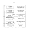
- FIGS. 13 a -13 b are effectivaly flow charts showing the different steps of a process to create segtons grouped within one or several nanolayers forming the seg-matter according to the parallel invention.
- the nanoscale unit according to the present invention is an elemental unity that is constituted and conditioned around the elemental unity of crystalline silicon lattice containing a structural point defect called divacancy.
- These nanoscale units called segtons are advantageously and necessarily coupled to their physical surrounding that is strictly physically conditioned and are usefully placed within the converter from the viewpoint of the incident light radiation and absorption.
- Segton is constituted on the basis of the divacancy being quasi-permanently in a doubly negative charge state and is conditioned by its physical neighborhood.
- the usually harmful defect can be advantageously transformed into a useful nanoobject that has an electron energy-level set adjusted to the low-energy secondary generation and multiplication in silicon converters.
- the segton is able to provide its host material or matrix into a set of specific electron energy levels that distribution and dynamics allow continuous and sufficiently ultra-rapid conversion cycle.
- Segton results from a displacement of two atoms outside the crystalline, preferentially, silicon elementary unit that introduces prolonged electron bonds going through vacancy sites that are able to capture and localize free electrons occupying extrinsic energy levels, especially weakly bonded electrons.
- This displacement may be realized by an energy beam focused and deposited inside the semiconductor matter or lattice or matrix such as electron beam, ion beam, and other suitable irradiations.
- Segton contains short and long electron bonds such as dangling bonds of the molecular-like type that have to be permanently occupied by captured electrons in working converter. This corresponds to a specific permanent doubly negative electric-charge state that has to be assumed by segton immediate environment tailored to the nanoscale.
- the segton dynamics is extremely fast that is characterized by extremely short time constants. That signifies first of all an extremely fast dynamics of segton charging and discharging.
- the segton Being embedded in a given host material such as a semiconductor and preferentially the silicon, the segton allows the analogy with a nanocrystal that is able to tune energy levels being available for electrons.
- the ability of extraction and collection of electrons from segtons predestinates their technical applications.
- the unique segton feature i.e., combining the specific set of electron energy levels with an excellent electron conduction or transport distinguishes segton from other nanoscale transformations known up to nowadays.
- the preferred method of segton manufacture is based on buried amorphizatons nanovolumes that are wrapped around by a nanolayer grafted with divacancies during the process.
- a method of nanoscale transformation being able to fulfill several required conditions is based on a local amorphization of a previously crystalline semiconductor, preferentially silicon, using, for example, an ion beam.
- This processing allow a good localization of the point defects in the device space and can lead to a self-organization in an ordered superlattice due to the built-in strain field that is induced by dilatation forces at the c-Si/a-Si interface.
- the strain field governs the segton distribution during the thermal treatment.
- the amorphization produces rough or rugged a-Si/c-Si heterointerfaces and small a-Si inclusions in c-Si and c-Si inlusions in a-Si.
- the subsequent annealing cycle preferentially at about 500-550° C. takes the form of a solid state epitaxy and leads to clear, atom scale separation of both silicon phases (crystalline and amorphized) as well as to sharp planar a-Si/c-Si heterointerfaces.
- the same annealing cycle leads to the creation of more or less planar nanolayers that are smoothly wrapping the each amorphized grain.
- the said nanolayers of 3-5-10 nm thick are uniform, without any faults and inequalities and contains numerous and ordered segtons forming together a seg-matter which is silicon based metamaterial MTM.
- the limited displacement of Si atoms inside the elementary unit requires relatively very low energies per displaced atom (about 2.5 eV/atom). Such displacement of two atoms leads introduces prolonged electron bonds that can capture and localize electrons. To become technically useful the divacancy has to contain permanently 4 captured electrons where one of them is weakly bonded. This is possible, for example, in a heavily n-type doped material, e.g., provided with the high phosphorous doping (Si:P).
- insertions/substructures substructures implantation providing the converter in fine in reservoirs of segtons and seg-matter appropriate processing—one beam or more beams, energies, doses, angle(s) of the incidence, species, the order, looking for interactions, conditions, for example, target temperature, shaping with respect of further processing by eventual superposition of successive treatments, balance of overall processing, previous and further processing steps, specific conditions structure the cycle(s) of thermal treatment has(ve): at first place, to figure the two neighboring areas on both sides of the c-Si/a-Si heterointerface to order their extreme mismatch just after the amorphization to dissolve or restructure inclusions of opposite phases that is a-Si in c-Si and c-Si in a-Si to release the crystalline ⁇ c-Si> phase stuffed with numerous point defects and to uniform the distribution of the crystalline ⁇ c-Si> phase that has surround homogeneously
- segtons have to be sufficiently numerous and well distributed, placed in a well-defined nanospace, permanently conserve their useful charge state, allow temperature processing during device manufacturing without threat of their erasing or transformation. Contrary to divacances that are normally spread sparsely and randomly in the semiconductor, preferentially silicon, material, segtons representing technical objects, are concentrated in a well delimited nanolayer nanospace.
- the recrystallized material has a dominant crystalline behavior but contains numerous displaced atoms that are distributed rather uniformly.
- the controlled recrystallization has to respect several conditions concerning the recrystallization or the solid state epitaxy rate, temperature, delay to conserve numerous displaced atoms in their new positions and to avoid additional harmful structural damages resulting, for example, from too violent atom movements.
- This processing allows a good localization of the transformed material from the absorption viewpoint.
- the a-Si/c-Si heterointerface transition zone gathers numerous segtons, up to the density of about 10 20 cm ⁇ 3 , which are trapped within the dilatation or tensile strain field.
- This tensile field plays, at least, four roles:
- the ion implantation and subsequent processing allows fulfillment of other requirements as the permanent double negative charge state, the spatial disposition, the electron transport etc . . . . All these transformations lead to metamaterial build from segtons.
- the segton double negative charge state allows a low-energy electron transition/release between the divacancy/segton energy level in the upper half of the indirect Si band gap and the conduction band.
- the concentration of doping impurity for n-type semiconductor has to be large enough such as 10 18 to 10 21 atoms cm ⁇ 3 , to charge and recharge all numerous divacances.
- the technically useful double negative charge state has to be instantaneously renewable just after an electron emission and extraction.
- FIGS. 1 and 2 bear on the specific model of the segton based on a divacancy conditioned by physical fields symbolized by triple arrows ( FIG. 3 ), which are at least: doping impurities, a built-in electric field and a built-in stress field. Segtons result from suitable and complex defects conditioning.
- atom engineering elemental crystalline unit of silicon
- a weak bond is indicated by a solid black line appearing between b-b′ atoms ( FIG. 2 ). This line goes through c-c′ vacancies. There are three equivalent weak bonds through c-c′ vacancies: a-a′, b-b′ and d-d′.
- a Jahn-Teller distortion appears in the metamaterial Symbols in figures: Cartesian coordinates (x, y, z), [1,0,0] crystalline axis orientations, and vector P, angle ⁇ .
- FIG. 3 Four other segtons ( FIG. 3 ) symbolize the background of the ordered segton superlattice, i.e., their distribution inside the metamaterial MTM nanolayer.
- the segtons result from suitable and complex defects conditioning.
- the scheme of a divacancy conditioned by physical fields is symbolized by the triple arrows:
- FIG. 4 is a mere general and schematic view of a model of an example of a metamaterial MTM nanolayer with smoothly varying density of segtons; the higher density is closer to the realizing amorphous phase decreasing in the crystalline phase.
- FIGS. 5 to 8 show scheme of a nanoscale Si-layered system containing a metamaterial ( ⁇ c-Si> nanolayers) of nanostructured silicon which has been obtained by doping, ion implantation and adequate thermal treatment (drawing not to scale).
- FIG. 6 shows an example of a device with a planar architecture containing one of the possible combinations exploiting the nanoscale Si-layered systems with a Si metamaterial.
- the presented device is provided in a back surface field (BSF).
- BSF back surface field
- FIGS. 7 and 8 schematize a top of a crystalline Si wafer containing a buried substructure being able to combine optoelectronic features (not to scale).
- Simplest nanoscale transformations lead to the superposition of several specific layers and especially a silicon metamaterial; three nanolayers denoted ⁇ c-Si>; one at the SiO 2 /Si interface and two at a-Si/c-Si interfaces that are labeled in the figure as top/and lower active nanostructures.
- One of the specific effects i.e. the surface free-carrier reservoir, results from the carrier collection limit (CCL) which appears at the upper a-Si/c-Si interface.
- CCL carrier collection limit
- FIG. 9 is a cross section TEM image presenting an example of the planar multi-interface substructure realized by controlled recrystallization of the amorphized phase that is buried by ion-implantation and post-implantation processing within a crystalline Si. Details are explained on the right graph illustrating 2D nanoscale Si-layered system.
- FIG. 10 is a schematic illustration of the electron energy band and electron energy level sets of:
- the heavily doped n-type strained crystalline nanolayers denoted ⁇ c-Si> which are two at active a-Si/c-Si heterointerfaces and one at the superficial SiO 2 /Si heterointerface, contain a Si metamaterial
- FIG. 11 is a schematic illustration of the electron energy set with an additional light-to-electricity conversion mechanism possible due to this set: low-energy (0.274 eV) impact ionization of segtons with the photon energy >1.1+n ⁇ 0.274 eV, where n (an integer number) represents the multiplication order with specific energy of 0.274 eV.
- FIG. 12 illustrates the comparison of theoretical orders electron multiplication determined on the basis of
- FIG. 13 presents step by step the whole process to create segtons and the grouping of segtons to form one or several nanolayers of segtons.
Landscapes
- Photovoltaic Devices (AREA)
- Chemical & Material Sciences (AREA)
- Crystallography & Structural Chemistry (AREA)
- Life Sciences & Earth Sciences (AREA)
- Sustainable Development (AREA)
- Silicon Compounds (AREA)
Priority Applications (1)
| Application Number | Priority Date | Filing Date | Title |
|---|---|---|---|
| US14/890,603 US9722121B2 (en) | 2013-05-14 | 2014-05-13 | Nanostructured units formed inside a silicon material and the manufacturing process to perform them therein |
Applications Claiming Priority (3)
| Application Number | Priority Date | Filing Date | Title |
|---|---|---|---|
| US201361855343P | 2013-05-14 | 2013-05-14 | |
| US14/890,603 US9722121B2 (en) | 2013-05-14 | 2014-05-13 | Nanostructured units formed inside a silicon material and the manufacturing process to perform them therein |
| PCT/IB2014/001973 WO2014203080A2 (en) | 2013-05-14 | 2014-05-13 | Nanostructured units formed inside a silicon material and the manufacturing process to perform them therein |
Publications (2)
| Publication Number | Publication Date |
|---|---|
| US20160099368A1 US20160099368A1 (en) | 2016-04-07 |
| US9722121B2 true US9722121B2 (en) | 2017-08-01 |
Family
ID=51862633
Family Applications (1)
| Application Number | Title | Priority Date | Filing Date |
|---|---|---|---|
| US14/890,603 Active US9722121B2 (en) | 2013-05-14 | 2014-05-13 | Nanostructured units formed inside a silicon material and the manufacturing process to perform them therein |
Country Status (7)
| Country | Link |
|---|---|
| US (1) | US9722121B2 (da) |
| EP (1) | EP2997604B1 (da) |
| CN (1) | CN105229799B (da) |
| DK (1) | DK2997604T3 (da) |
| FR (1) | FR3005790A1 (da) |
| PL (1) | PL2997604T3 (da) |
| WO (1) | WO2014203080A2 (da) |
Cited By (3)
| Publication number | Priority date | Publication date | Assignee | Title |
|---|---|---|---|---|
| US20160155869A1 (en) * | 2013-07-19 | 2016-06-02 | Segton Adt Sas | System of architecture and related built-in nanomembranes for the emitter of a light-to-electricity all-silicon converter for the giant photocnversion and the method of its manufacture |
| US10886422B2 (en) | 2013-05-14 | 2021-01-05 | Segton Advanced Technology | Grouped nanostructured units system forming a metamaterial |
| US11437532B2 (en) | 2017-06-01 | 2022-09-06 | Segton Advanced Technology | Method for the production of a light-to-electricity converter made entirely from silicon for a giant photoconversion |
Citations (3)
| Publication number | Priority date | Publication date | Assignee | Title |
|---|---|---|---|---|
| WO2010089624A1 (en) | 2009-02-06 | 2010-08-12 | Kuznicki Zbigniew T | Methods for producing photovoltaic material and device able to exploit high energy photons |
| WO2012131496A2 (en) | 2011-03-25 | 2012-10-04 | Kuznicki Zbigniew | Improved emitter structure based on silicone components to be used in a photovoltaic converter and a method for production of the photovoltaic device |
| US20160155869A1 (en) * | 2013-07-19 | 2016-06-02 | Segton Adt Sas | System of architecture and related built-in nanomembranes for the emitter of a light-to-electricity all-silicon converter for the giant photocnversion and the method of its manufacture |
-
2014
- 2014-05-13 DK DK14795861.5T patent/DK2997604T3/da active
- 2014-05-13 CN CN201480028263.1A patent/CN105229799B/zh not_active Expired - Fee Related
- 2014-05-13 PL PL14795861T patent/PL2997604T3/pl unknown
- 2014-05-13 EP EP14795861.5A patent/EP2997604B1/en active Active
- 2014-05-13 US US14/890,603 patent/US9722121B2/en active Active
- 2014-05-13 WO PCT/IB2014/001973 patent/WO2014203080A2/en not_active Ceased
- 2014-05-13 FR FR1401072A patent/FR3005790A1/fr not_active Withdrawn
Patent Citations (5)
| Publication number | Priority date | Publication date | Assignee | Title |
|---|---|---|---|---|
| WO2010089624A1 (en) | 2009-02-06 | 2010-08-12 | Kuznicki Zbigniew T | Methods for producing photovoltaic material and device able to exploit high energy photons |
| US20110162700A1 (en) * | 2009-02-06 | 2011-07-07 | Kuznicki Zbigniew T | Methods for producing photovolaic material and device able to exploit high energy photons |
| WO2012131496A2 (en) | 2011-03-25 | 2012-10-04 | Kuznicki Zbigniew | Improved emitter structure based on silicone components to be used in a photovoltaic converter and a method for production of the photovoltaic device |
| US20130340819A1 (en) * | 2011-03-25 | 2013-12-26 | Zbigniew Kuznicki | Emitter structure based on silicon components to be used in a photovoltaic converter and a method for production of the photovoltaic device |
| US20160155869A1 (en) * | 2013-07-19 | 2016-06-02 | Segton Adt Sas | System of architecture and related built-in nanomembranes for the emitter of a light-to-electricity all-silicon converter for the giant photocnversion and the method of its manufacture |
Cited By (4)
| Publication number | Priority date | Publication date | Assignee | Title |
|---|---|---|---|---|
| US10886422B2 (en) | 2013-05-14 | 2021-01-05 | Segton Advanced Technology | Grouped nanostructured units system forming a metamaterial |
| US20160155869A1 (en) * | 2013-07-19 | 2016-06-02 | Segton Adt Sas | System of architecture and related built-in nanomembranes for the emitter of a light-to-electricity all-silicon converter for the giant photocnversion and the method of its manufacture |
| US10020408B2 (en) * | 2013-07-19 | 2018-07-10 | Segton Advanced Technology | System of architecture and related built-in nanomembranes for the emitter of a light-to-electricity all-silicon converter for the giant photoconversion and the method of its manufacture |
| US11437532B2 (en) | 2017-06-01 | 2022-09-06 | Segton Advanced Technology | Method for the production of a light-to-electricity converter made entirely from silicon for a giant photoconversion |
Also Published As
| Publication number | Publication date |
|---|---|
| PL2997604T3 (pl) | 2020-11-30 |
| WO2014203080A4 (en) | 2015-06-25 |
| US20160099368A1 (en) | 2016-04-07 |
| EP2997604B1 (en) | 2020-07-08 |
| DK2997604T3 (da) | 2020-09-14 |
| FR3005790A1 (fr) | 2014-11-21 |
| WO2014203080A3 (en) | 2015-04-16 |
| CN105229799A (zh) | 2016-01-06 |
| WO2014203080A2 (en) | 2014-12-24 |
| CN105229799B (zh) | 2019-06-14 |
| EP2997604A2 (en) | 2016-03-23 |
Similar Documents
| Publication | Publication Date | Title |
|---|---|---|
| TWI474494B (zh) | 多晶矽發射極太陽能電池所用的圖案化摻雜 | |
| US10886422B2 (en) | Grouped nanostructured units system forming a metamaterial | |
| EP2394308B1 (en) | Methods for producing photovoltaic material able to exploit high energy photons | |
| EP2997604B1 (en) | Nanostructured units formed inside a silicon material and the manufacturing process to perform them therein | |
| TW201519289A (zh) | 矽內的高濃度摻雜 | |
| CN103503158A (zh) | 用于光伏转换器的基于有机硅成份的改进的发射极结构以及制造所述光伏装置的方法 | |
| CN104900733A (zh) | 一种基于GaSb的In1-xGaxSb/GaSb应变量子阱中间能带热光伏电池及其制备方法 | |
| EP3022776B1 (en) | System of architecture and related built-in nanomembranes for the emitter of a light-to-electricity all-silicon converter for the giant photoconversion and the method of its manufacture | |
| US11329180B2 (en) | Entire solar spectrum multiplying converting platform unit for an optimal light to electricity conversion | |
| US11437532B2 (en) | Method for the production of a light-to-electricity converter made entirely from silicon for a giant photoconversion | |
| Kuznicki | Multi-interface novel devices: model with a continuous substructure | |
| US20120322192A1 (en) | Method of defect reduction in ion implanted solar cell structures | |
| Nakamura et al. | Selective emitter N-pert solar cell using NON mass separatION type ION implantatION | |
| KUZNICKI et al. | Buried in Single-Crystal Si by Implantation Processing |
Legal Events
| Date | Code | Title | Description |
|---|---|---|---|
| AS | Assignment |
Owner name: SEGTON ADVANCED TECHNOLOGY, FRANCE Free format text: ASSIGNMENT OF ASSIGNORS INTEREST;ASSIGNORS:KUZNICKI, ZBIGNIEW;MEYRUEIS, PATRICK;REEL/FRAME:037154/0044 Effective date: 20151106 |
|
| STCF | Information on status: patent grant |
Free format text: PATENTED CASE |
|
| FEPP | Fee payment procedure |
Free format text: ENTITY STATUS SET TO UNDISCOUNTED (ORIGINAL EVENT CODE: BIG.); ENTITY STATUS OF PATENT OWNER: LARGE ENTITY |
|
| MAFP | Maintenance fee payment |
Free format text: PAYMENT OF MAINTENANCE FEE, 4TH YR, SMALL ENTITY (ORIGINAL EVENT CODE: M2551); ENTITY STATUS OF PATENT OWNER: SMALL ENTITY Year of fee payment: 4 |
|
| FEPP | Fee payment procedure |
Free format text: PETITION RELATED TO MAINTENANCE FEES GRANTED (ORIGINAL EVENT CODE: PTGR); ENTITY STATUS OF PATENT OWNER: LARGE ENTITY |
|
| FEPP | Fee payment procedure |
Free format text: PETITION RELATED TO MAINTENANCE FEES GRANTED (ORIGINAL EVENT CODE: PTGR); ENTITY STATUS OF PATENT OWNER: LARGE ENTITY |
|
| MAFP | Maintenance fee payment |
Free format text: PAYMENT OF MAINTENANCE FEE UNDER 1.28(C) (ORIGINAL EVENT CODE: M1559); ENTITY STATUS OF PATENT OWNER: LARGE ENTITY |
|
| FEPP | Fee payment procedure |
Free format text: PETITION RELATED TO MAINTENANCE FEES GRANTED (ORIGINAL EVENT CODE: PTGR); ENTITY STATUS OF PATENT OWNER: LARGE ENTITY |
|
| MAFP | Maintenance fee payment |
Free format text: PAYMENT OF MAINTENANCE FEE, 8TH YEAR, LARGE ENTITY (ORIGINAL EVENT CODE: M1552); ENTITY STATUS OF PATENT OWNER: LARGE ENTITY Year of fee payment: 8 |