US9797965B2 - Fast hall effect measurement system - Google Patents
Fast hall effect measurement system Download PDFInfo
- Publication number
- US9797965B2 US9797965B2 US14/996,719 US201614996719A US9797965B2 US 9797965 B2 US9797965 B2 US 9797965B2 US 201614996719 A US201614996719 A US 201614996719A US 9797965 B2 US9797965 B2 US 9797965B2
- Authority
- US
- United States
- Prior art keywords
- test
- frequency
- voltage
- excitation
- magnetic field
- Prior art date
- Legal status (The legal status is an assumption and is not a legal conclusion. Google has not performed a legal analysis and makes no representation as to the accuracy of the status listed.)
- Active
Links
Images


Classifications
-
- G—PHYSICS
- G01—MEASURING; TESTING
- G01R—MEASURING ELECTRIC VARIABLES; MEASURING MAGNETIC VARIABLES
- G01R33/00—Arrangements or instruments for measuring magnetic variables
- G01R33/12—Measuring magnetic properties of articles or specimens of solids or fluids
-
- G—PHYSICS
- G01—MEASURING; TESTING
- G01R—MEASURING ELECTRIC VARIABLES; MEASURING MAGNETIC VARIABLES
- G01R33/00—Arrangements or instruments for measuring magnetic variables
- G01R33/02—Measuring direction or magnitude of magnetic fields or magnetic flux
- G01R33/06—Measuring direction or magnitude of magnetic fields or magnetic flux using galvano-magnetic devices
- G01R33/07—Hall effect devices
- G01R33/072—Constructional adaptation of the sensor to specific applications
Definitions
- the present invention relates generally to a method for measuring materials properties, and more particularly to a method for measuring Hall effect voltage.
- Hall voltage is proportional to the magnetic field and current, and depends inversely on the thickness of the material.
- the proportionality constant is called the Hall coefficient.
- the Hall coefficient and resistivity of the material can be related to the material properties carrier density and carrier mobility.
- the sign of the Hall voltage is the same as the sign of the charge of the carriers and thus provides a determination of carrier type (holes or electrons).
- the measured Hall voltage is zero when the applied magnetic field is zero.
- the voltage measured in a practical experiment is typically not zero, and includes a misalignment voltage and a thermal electric voltage.
- the misalignment voltage is proportional to the resistivity of the material, the current, and a factor that depends on the geometry. This factor converts resistivity to resistance between two Hall voltage probes.
- the thermal electric voltage arises from contacts between two different materials and is dependent on the thermal gradients present.
- One method for measuring Hall effect involves application of a DC magnetic field to piece of material.
- the effects of the thermal electric voltage can be removed by changing the direction of the current applied across the material and measuring the voltage for both current directions.
- Thermal electric voltage does not depend on current.
- the effect of the thermal electric voltage is removed by subtracting the measured voltage at the two different currents.
- misalignment voltage can be removed by changing the direction of the magnetic field and measuring the voltage for both field directions. Misalignment voltage does not depend on magnetic field. Thus, the effect of the misalignment voltage is removed by subtracting the measured voltage at the two different currents.
- the DC-field method may be advantageous for high-mobility materials, it often fails to provide accurate measurements for low-mobility materials, i.e., materials with a mobility less than 1 cm 2 /Vs.
- low-mobility materials the difference between the voltage measurements at each field direction becomes much smaller compared to the misalignment voltage. As a result, noise in the system can dominate the measurement and produce inaccurate results. Accordingly, Hall measurements using the DC-field method on low-mobility materials often give inconsistent values and carrier signs.
- Another method of measuring Hall effect uses an AC magnetic field. Because the misalignment voltage is not dependent on the magnetic field, it will remain a DC voltage while the Hall voltage is an AC voltage. A DC current is still used in this method, meaning that the thermal electric voltage also remains a DC voltage. A lock-in amplifier can then be used to easily separate the AC and DC voltages and thus the misalignment voltage from the Hall voltage.
- the AC-field method solves some of the problems inherent in the DC-field method. Particularly, the separation of voltages in frequency space allows for much easier detection of smaller voltage differences, for example when measuring low-mobility carriers.
- the AC-field method suffers from a large drawback: in actual use it can be slow.
- the speed is determined by the frequency of the magnetic field.
- the highest operating frequency can be approximately 0.1 Hz (10 seconds per cycle), as determined by the inductance of the magnet.
- a lock-in amplifier uses 6 cycles of input for best averaging of the output signal.
- a single Hall voltage measurement may take 60 seconds.
- adding current reversal, which is required to remove the thermal electric voltages and phase errors a total of 6 measurements are required, making the time to measure a Hall voltage 6 minutes. In practice, this Hall measurement is repeated from 10 to 100 times to get average values and an estimation of statistical variations. In sum, full measurement of a single material can take up to 10 hours under this method.
- the Hall voltage will be small. To measure such materials, increasing the current will increase the Hall voltage. However, when the current is increased, self-heating can cause the temperature of the material to change. Specifically, the sample and contacts will have some resistance and power will be dissipated in the sample. This power will heat up the sample.
- the misalignment voltage is proportional to the resistivity of the material. As the temperature of the sample changes, the resistance changes and hence the misalignment voltage changes. In effect, a term that was a DC signal becomes a time dependent signal that will be detected by the lock-in amplifier in addition to the Hall voltage. The slowly-changing misalignment voltage will look like noise in the measurement. Additional noise comes from the Johnson-Nyquist noise due to material resistance. These two noise contributions to the measurements limit the ability of the AC field Hall method to measure small Hall voltages.
- a system and method is needed for more quickly and accurately measuring Hall voltages, particularly for low-mobility materials.
- Embodiments of the present invention comprise systems and methods of measuring the Hall effect voltage of a material.
- a first test state is provided alternating a first test parameter at a first frequency.
- a second test state is provided alternating a second test parameter at a second frequency.
- the first test parameter is one of a test excitation, a location of the test excitation, a direction of a magnetic field and a location of the magnetic field
- the second test parameter is another of the test excitation, the location of the test excitation, the direction of a magnetic field and the location of the magnetic field.
- a system for measuring the Hall effect voltage of a material includes a magnet, test excitation mechanism, a voltage measuring device and a control configured to provide a first test state alternating a first test parameter at a first frequency and a second test state alternating a second test parameter at a second frequency.
- the first test parameter is one of a test excitation, a location of the test excitation, a direction of a magnetic field and a location of the magnetic field
- the second test parameter is another of the test excitation, the location of the test excitation, the direction of a magnetic field or the location of the magnetic field.
- FIGS. 1 a -1 h are exemplary schematic diagrams of several different states of a Hall measurement device according to the present invention.
- FIG. 2 is a signal output from a first exemplary Hall measurement device for a high-mobility material
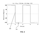
- FIG. 3 is a signal output from the first exemplary Hall measurement device for a low-mobility material
- FIG. 4 is a signal output from a second exemplary Hall measurement device for a low-mobility material according to the present invention.
- FIG. 5 is the signal output of FIG. 4 after exemplary conditioning according to the present invention.
- FIG. 6 is a flow chart illustrating a method of measuring a Hall voltage according to the present invention.
- FIG. 7 is an exemplary system for measuring a Hall voltage according to the present invention.
- FIGS. 8 a and 8 b are schematic diagrams of exemplary material shapes measured by a Hall sensing device according to the present invention.
- FIGS. 1 a -1 h illustrate several states of two exemplary systems for detecting Hall voltage in an exemplary piece of material 100 .
- a resulting Hall voltage V H dependent on the material's Hall factor R H can be measured perpendicular to the plane created by the current and magnetic field.
- Reference axes 101 and 103 illustrate the physical relationship between these elements in two different configurations.
- the actual measured voltage V m includes other voltage components.
- a misalignment voltage V ma may appear based on the resistivity ⁇ , and geometrical factor ⁇ of the piece of material
- the measurement may include a thermal-electric voltage V te . With those components added, the measured voltage should be equal to:
- V m I ⁇ R H ⁇ B t + I ⁇ ⁇ t + V te
- the exemplary piece of material 100 of FIGS. 1 a -1 d is substantially square in shape, though as explained more fully herein, other shapes may be used.
- the piece of material 100 includes four contact points, 102 , 104 , 106 and 108 , arranged around outer edges of the material 100 , creating two pairs of generally opposite contact points.
- the piece of material may be any material for which Hall measurement is desired. Generally the thickness of the material may be any size but for practical measurements the thickness should be less than 2 mm. Smaller thickness will increase the Hall voltage, but will also increase the misalignment voltage.
- a current flow I 110 runs in the direction indicated by the arrow.
- a magnetic field B (not shown except in axes 101 ) is directed perpendicular to the surface area of the piece of material 100 .
- FIG. 1 a illustrates a first measuring state 120 .
- the current I 110 runs from contact point 106 , through the material 100 , to contact point 102 .
- a first voltage V m 1 130 is measured across contact points 104 and 108 and may be defined as follows:
- V m 1 I ⁇ R H ⁇ B t + I ⁇ ⁇ t + V te 1
- FIG. 1 b illustrates a second measuring state 122 .
- state 122 the same current I 110 now runs from contact point 108 , through the material 100 , to contact point 104 and a second voltage V m 2 132 is measured across contact points 106 and 102 .
- the Onsager relationship and H. H. Sample (Sample, H. H. and Bruno, W. J. and Sample, S. B. and Sichel, E. K., Journal of Applied Physics, 61, 1079-1084 (1987)) teaches us that the change in position of the current flow I 110 relative to the magnetic field B causes the above equation for V m 1 to change such that B is replaced with ⁇ B. Also, because the voltage leads are on different contact points, the thermal voltage V te 2 will be different, leading to the following equation:
- V m 2 - I ⁇ R H ⁇ B t + I ⁇ ⁇ t + V te 2
- FIG. 1 c illustrates a third measuring state 124 .
- state 124 the same current I 110 now runs from contact point 102 , through the material 100 , to contact point 106 and a third voltage V m 3 134 is measured across contact points 104 and 108 .
- the reversal of current flow I 110 relative to the first state 120 will cause the current I 110 to be negative in the equation, but because the same contact points are used, the thermal electric voltage will be the same V te 1 as in state 120 .
- the following equation defines state 124 :
- V m 3 - I ⁇ R H ⁇ B t - I ⁇ ⁇ t + V te 1
- FIG. 1 d illustrates a fourth measuring state 126 .
- state 126 the same current I 110 now runs from contact point 104 , through the material 100 , to contact point 108 and a fourth voltage V m 4 136 is measured across contact points 102 and 106 .
- the reversal of current flow I 110 relative to the second state 122 will again cause the current I 110 to be negative in the equation, but because the same contact points are used, the thermal electric voltage will be the same V te 2 as in that state.
- the change in position of the current flow I 110 relative to the magnetic field B causes the equation to change such that B is replaced with ⁇ B:
- V m 4 I ⁇ R H ⁇ B t - I ⁇ ⁇ t + V te 2
- the Hall voltage for the piece of material 100 can then be calculated from the above equations as V m 1 ⁇ V m 2 ⁇ V m 3 +V m 4 , which will remove the misalignment and thermal-electric voltages from the equation.
- Switching between states 120 , 122 , 124 and 126 requires only switching contact points for voltage measurement and current flow. Because no field reversal is necessary, the time for polarity reversal of large magnets is no longer an issue.
- FIGS. 1 e -1 h illustrate this alternate embodiment wherein a specific voltage 142 a , 144 a , 146 a and 148 a is applied with resulting currents 142 b , 144 b , 146 b and 148 b generated, and resulting voltages V m 140 are measured.
- the above method may still fail to accurately measure Hall voltage in low-mobility carriers with high misalignment voltage.
- Hall voltage and misalignment voltage will change at the same frequency, but with a phase shift between the two.
- the misalignment voltage is the same order of magnitude or smaller than the Hall voltage.
- the separation in phase space is sufficient to get a measurement of Hall voltage without contribution from the misalignment voltage.
- An exemplary voltage measurement for a high-mobility carrier is shown in FIG. 2 .
- the misalignment voltage seen as the change in amplitude at point 200 and similar points of the signal, is easily separable from the Hall voltage, which is seen as the large change in amplitude at 202 and similar points.
- the misalignment voltage is typically very large compared to the Hall voltage. Accordingly, it may be difficult, if not impossible, to separate the Hall voltage from the misalignment voltage, as both occur at the same frequency.
- An exemplary voltage measurement is shown in FIG. 3 . As can be seen, the misalignment voltage, seen as the change in amplitude at point 300 and similar points of the signal, dominates the square wave. By contrast, the Hall voltage, the tiny change in amplitude at 302 and similar points, will be very difficult to measure.
- the above problem in measuring Hall voltage for low-mobility carriers can be overcome by modifying the above method to vary the frequency between the misalignment voltage and Hall voltage.
- the misalignment voltage which does not depend on the magnetic field, remains constant between states 120 and 122 and between states 124 and 126 , while at the same time the Hall Voltage, which does depend on the magnetic field, reverses sign.
- non-sequential switching techniques create different frequencies between the misalignment voltage and Hall voltage.
- the Hall voltage and misalignment voltage are set to differing frequencies.
- FIG. 4 shows an exemplary voltage measurement technique using an exemplary switching pattern as described above. While this misalignment voltage 400 is still very large compared to the Hall voltage 402 , the Hall voltage 402 is now toggled at a different frequency than the misalignment voltage 400 . A demodulation may then be used, for example a double demodulation, on the signal to separate out the Hall voltage, followed by an amplifier, e.g., an AC-coupled amplifier, to measure the Hall voltage. An amplified version of the demodulated Hall voltage from FIG. 4 is shown in FIG. 5 . As can be seen, the Hall voltage is now easily measurable.
- a demodulation may then be used, for example a double demodulation, on the signal to separate out the Hall voltage, followed by an amplifier, e.g., an AC-coupled amplifier, to measure the Hall voltage.
- An amplified version of the demodulated Hall voltage from FIG. 4 is shown in FIG. 5 . As can be seen, the Hall voltage is now easily measurable.
- the different measurements are more easily discernible from the voltage measurement of FIG. 4 .
- the switching between first and seconds states occurs over the period 410 (or n cycles as used below) and the switching between third and fourth states occurs over the period 412 (or m cycles as used below).
- the entire period of the measurement 414 corresponds to the total number of cycles (p, as used below) for the measurement.
- step 610 voltage is measured in a first state, with a current flowing in a first direction across the material and a voltage signal measured across a perpendicular direction.
- step 620 voltage is measured in a second state where the current is switched to flow perpendicular to its previous direction and the voltage signal is measured perpendicular to the new current direction.
- Steps 610 and 620 are repeated n times at step 630 before moving to step 640 .
- the repetition count n may be any number of times, for example in the range of 1-10 times, but may be greater.
- Step 640 the current is switched to flow in the opposite direction as in step 610 , with the voltage signal again measured in this third state across a perpendicular direction.
- step 650 voltage is measured in a fourth state where the current is switched to flow perpendicular to its previous direction and opposite the current of step 620 .
- the voltage signal is measured perpendicular to the new current direction.
- Steps 640 and 650 are repeated m times at step 660 .
- the repetition count m may be any number of times, for example in the range of 1-10 times, but may be greater.
- the method then returns to step 610 and steps 610 - 660 are repeated as described above p times at step 670 , until the desired quantity of measurement has been completed.
- the repetition count p may be any number of times, for example in the range of 1-10 times, but may be greater.
- exemplary corresponding states are shown.
- a measurement can toggle between states 120 and 122 n times, then toggle between states 124 and 126 m times, repeating the process for a total of p times.
- n and m may be equal, resulting in two frequencies, one each for Hall voltage and misalignment voltage, or n and m may be different, creating two frequencies each for the two voltages.
- the totality of measurements p may not be much larger than each of the individual sets of cycles n and m, and in other cases p may be much larger than n and m, providing for a larger measurement sample.
- the individual measurements at each state are recorded in time to create a continuous voltage-measurement signal.
- step 670 the method moves to step 680 where the measured signal is demodulated, e.g., by double demodulation.
- step 690 the demodulated signal is amplified, e.g., by AC-coupled amplification.
- FIG. 6 shows steps 610 and 620 being repeated n times.
- the number of repeated cycles n can be any number sufficient to effectuate practical demodulation.
- FIG. 6 shows steps 640 and 650 being repeated a different number of times, i.e., m times, it is contemplated that the number of cycles repeated between steps 640 and 650 may be the same as the number of cycles repeated between steps 610 and 620 , i.e., n times.
- FIG. 7 shows a schematic diagram of an exemplary system 700 according to the present invention used to measure the Hall voltage of a piece of material 702 .
- the system 700 includes a magnet 704 for creating a magnetic field.
- the magnet 704 can be any suitable magnet, with the understanding that more powerful magnets may be necessary to induce a measurable Hall voltage in heavily doped materials. For example, magnets capable of generating a 1 T or greater field, and for some applications, superconducting magnets of 9 T or greater may be necessary.
- magnets capable of generating a 1 T or greater field, and for some applications, superconducting magnets of 9 T or greater may be necessary.
- typical values for the n cycle times would be 0.5 to 5 seconds and typical values for the m cycle times would also be 0.5 to 5 seconds, though other values are contemplated, such as, but not limited to, 0.5 seconds each for n and m cycle times, 1 second each for m and n cycle times, 5 seconds each for n and m cycle times or 0.5 seconds for n cycle times and 1.5 seconds for m cycle times.
- the value of n and m for these cycle times might be on the order of 100. This provides a high quality Hall voltage measurement in 10 seconds or less. This time should be compared to the approximately 1 hour that a similar-quality Hall measurement using the AC field method would require. This is a factor of over 300 improvement in the measurement time of the sample.
- the exemplary system 700 also includes current source 706 , which can be any standard DC current source, [for example Keithley 6220].
- the system 700 further includes a voltage-measuring device 708 capable of measuring a voltage signal, [such as Signal Recovery 7230 lock in amplifiers].
- the current source 706 and voltage-measuring device 708 are connected to a controller 710 .
- the controller 710 may be, for example, an array of switches.
- the controller 710 is in turn connected to four contact points, 720 , 722 , 724 , and 726 of material 702 .
- the controller 710 is configured to change which of the contact points 720 , 722 , 724 , and 726 are connected to the current source 706 and which are connected to the voltage measuring device 708 at any given time, facilitating fast switching of the states of the above-described methods.
- the method described herein uses a current source as the excitation for the measurement.
- a current source such as a Keysight B2987A electrometer
- a current meter such as a Keithley 6485
- FIGS. 8 a and 8 b depict two exemplary shapes for a piece of material measured according to the present invention.
- FIG. 8 a depicts a piece of material in a hall bar shape having contact points 802 , 804 , 806 , and 808 .
- FIG. 8 b depicts a piece of material in a Greek cross shape, having contact points 812 , 814 , 816 , and 818 .
Landscapes
- Physics & Mathematics (AREA)
- Condensed Matter Physics & Semiconductors (AREA)
- General Physics & Mathematics (AREA)
- Measuring Magnetic Variables (AREA)
- Hall/Mr Elements (AREA)
- Measurement Of Current Or Voltage (AREA)
- Investigating Or Analyzing Materials By The Use Of Magnetic Means (AREA)
- Investigating Or Analyzing Materials By The Use Of Electric Means (AREA)
Priority Applications (9)
| Application Number | Priority Date | Filing Date | Title |
|---|---|---|---|
| US14/996,719 US9797965B2 (en) | 2016-01-15 | 2016-01-15 | Fast hall effect measurement system |
| EP22172028.7A EP4060333B1 (fr) | 2016-01-15 | 2016-12-09 | Système de mesure d'effet hall rapide |
| KR1020187023520A KR102521705B1 (ko) | 2016-01-15 | 2016-12-09 | 고속 홀 효과 측정 시스템 |
| JP2018536502A JP6757038B2 (ja) | 2016-01-15 | 2016-12-09 | 高速ホール効果測定システム |
| EP16885412.3A EP3403083B1 (fr) | 2016-01-15 | 2016-12-09 | Système de mesure d'effet hall rapide |
| CN201680082029.6A CN108700554B (zh) | 2016-01-15 | 2016-12-09 | 快速霍尔效应测量系统 |
| PCT/US2016/065747 WO2017123353A1 (fr) | 2016-01-15 | 2016-12-09 | Système de mesure d'effet hall rapide |
| TW105143270A TWI736569B (zh) | 2016-01-15 | 2016-12-27 | 快速霍爾效應量測系統 |
| US15/782,067 US10073151B2 (en) | 2016-01-15 | 2017-10-12 | Fast hall effect measurement system |
Applications Claiming Priority (1)
| Application Number | Priority Date | Filing Date | Title |
|---|---|---|---|
| US14/996,719 US9797965B2 (en) | 2016-01-15 | 2016-01-15 | Fast hall effect measurement system |
Related Child Applications (1)
| Application Number | Title | Priority Date | Filing Date |
|---|---|---|---|
| US15/782,067 Continuation US10073151B2 (en) | 2016-01-15 | 2017-10-12 | Fast hall effect measurement system |
Publications (2)
| Publication Number | Publication Date |
|---|---|
| US20170205475A1 US20170205475A1 (en) | 2017-07-20 |
| US9797965B2 true US9797965B2 (en) | 2017-10-24 |
Family
ID=59311541
Family Applications (2)
| Application Number | Title | Priority Date | Filing Date |
|---|---|---|---|
| US14/996,719 Active US9797965B2 (en) | 2016-01-15 | 2016-01-15 | Fast hall effect measurement system |
| US15/782,067 Active US10073151B2 (en) | 2016-01-15 | 2017-10-12 | Fast hall effect measurement system |
Family Applications After (1)
| Application Number | Title | Priority Date | Filing Date |
|---|---|---|---|
| US15/782,067 Active US10073151B2 (en) | 2016-01-15 | 2017-10-12 | Fast hall effect measurement system |
Country Status (7)
| Country | Link |
|---|---|
| US (2) | US9797965B2 (fr) |
| EP (2) | EP3403083B1 (fr) |
| JP (1) | JP6757038B2 (fr) |
| KR (1) | KR102521705B1 (fr) |
| CN (1) | CN108700554B (fr) |
| TW (1) | TWI736569B (fr) |
| WO (1) | WO2017123353A1 (fr) |
Cited By (1)
| Publication number | Priority date | Publication date | Assignee | Title |
|---|---|---|---|---|
| US20180031648A1 (en) * | 2016-01-15 | 2018-02-01 | Lake Shore Cryotronics, Inc. | Fast hall effect measurement system |
Families Citing this family (4)
| Publication number | Priority date | Publication date | Assignee | Title |
|---|---|---|---|---|
| EP3415902B1 (fr) * | 2017-06-14 | 2023-12-27 | Rolls-Royce Corporation | Système de profilage de contrainte résiduelle non destructif utilisant une détection inductive |
| US11605778B2 (en) | 2019-02-07 | 2023-03-14 | Lake Shore Cryotronics, Inc. | Hall effect sensor with low offset and high level of stability |
| KR102210577B1 (ko) | 2019-07-26 | 2021-02-02 | 이종욱 | 에어컨 냉매 배관의 메쉬 감지방법 |
| CN111474456B (zh) * | 2020-04-14 | 2021-03-05 | 新磊半导体科技(苏州)有限公司 | 一种霍尔效应电压确定方法及霍尔测试系统 |
Citations (8)
| Publication number | Priority date | Publication date | Assignee | Title |
|---|---|---|---|---|
| US5424561A (en) | 1993-05-14 | 1995-06-13 | Kobe Steel Usa Inc. | Magnetic sensor element using highly-oriented diamond film and magnetic detector |
| US5604433A (en) | 1994-09-06 | 1997-02-18 | Deutsche Itt Industries Gmbh | Offset compensation for magnetic-field sensor with Hall effect device |
| US6064202A (en) | 1997-09-09 | 2000-05-16 | Physical Electronics Laboratory | Spinning current method of reducing the offset voltage of a hall device |
| US20010050557A1 (en) | 2000-05-03 | 2001-12-13 | Volker Kempe | Method for compensating mechanical stresses in measuring the magnetic field strength by hall sensors |
| US20020175679A1 (en) | 2000-12-04 | 2002-11-28 | Hoon Kim | Apparatus and method for measuring Hall effect |
| US20090045807A1 (en) | 2005-12-16 | 2009-02-19 | Asahi Kasei Emd Corporation | Position detection apparatus |
| US20140070796A1 (en) | 2012-09-07 | 2014-03-13 | Serge Reymond | Hall-effect-based angular orientation sensor and corresponding methods and devices |
| US20160061912A1 (en) * | 2012-09-27 | 2016-03-03 | Texas Instruments Deutschland Gmbh | Hall sensor excitation system |
Family Cites Families (11)
| Publication number | Priority date | Publication date | Assignee | Title |
|---|---|---|---|---|
| DE10032530C2 (de) * | 2000-07-05 | 2002-10-24 | Infineon Technologies Ag | Verstärkerschaltung mit Offsetkompensation |
| JP3285342B2 (ja) | 2000-08-02 | 2002-05-27 | 株式会社東陽テクニカ | ホール効果測定装置及びその方法 |
| KR100419005B1 (ko) * | 2000-12-04 | 2004-02-14 | 상록코리아 (주) | 홀 효과 측정장치 및 측정방법 |
| NL1024114C1 (nl) * | 2003-08-15 | 2005-02-16 | Systematic Design Holding B V | Werkwijze en inrichting voor het verrichten van metingen aan magnetische velden met gebruik van een hall-sensor. |
| GB0620307D0 (en) * | 2006-10-16 | 2006-11-22 | Ami Semiconductor Belgium Bvba | Auto-calibration of magnetic sensor |
| KR100937504B1 (ko) | 2008-11-12 | 2010-01-19 | 에코피아 주식회사 | 홀 효과 측정장치 |
| JP5314619B2 (ja) | 2010-02-19 | 2013-10-16 | 旭化成エレクトロニクス株式会社 | ホール起電力信号検出装置 |
| US9644939B2 (en) * | 2010-12-21 | 2017-05-09 | Capres A/S | Single-position hall effect measurements |
| US20140028305A1 (en) * | 2012-07-27 | 2014-01-30 | International Business Machines Corporation | Hall measurement system with rotary magnet |
| WO2014036664A1 (fr) * | 2012-09-07 | 2014-03-13 | Sensima Technology Sa | Capteur d'orientation angulaire à effet hall et procédés et dispositifs correspondants |
| US9797965B2 (en) * | 2016-01-15 | 2017-10-24 | Lake Shore Cryotronics, Inc. | Fast hall effect measurement system |
-
2016
- 2016-01-15 US US14/996,719 patent/US9797965B2/en active Active
- 2016-12-09 CN CN201680082029.6A patent/CN108700554B/zh active Active
- 2016-12-09 WO PCT/US2016/065747 patent/WO2017123353A1/fr not_active Ceased
- 2016-12-09 EP EP16885412.3A patent/EP3403083B1/fr active Active
- 2016-12-09 KR KR1020187023520A patent/KR102521705B1/ko active Active
- 2016-12-09 EP EP22172028.7A patent/EP4060333B1/fr active Active
- 2016-12-09 JP JP2018536502A patent/JP6757038B2/ja active Active
- 2016-12-27 TW TW105143270A patent/TWI736569B/zh active
-
2017
- 2017-10-12 US US15/782,067 patent/US10073151B2/en active Active
Patent Citations (8)
| Publication number | Priority date | Publication date | Assignee | Title |
|---|---|---|---|---|
| US5424561A (en) | 1993-05-14 | 1995-06-13 | Kobe Steel Usa Inc. | Magnetic sensor element using highly-oriented diamond film and magnetic detector |
| US5604433A (en) | 1994-09-06 | 1997-02-18 | Deutsche Itt Industries Gmbh | Offset compensation for magnetic-field sensor with Hall effect device |
| US6064202A (en) | 1997-09-09 | 2000-05-16 | Physical Electronics Laboratory | Spinning current method of reducing the offset voltage of a hall device |
| US20010050557A1 (en) | 2000-05-03 | 2001-12-13 | Volker Kempe | Method for compensating mechanical stresses in measuring the magnetic field strength by hall sensors |
| US20020175679A1 (en) | 2000-12-04 | 2002-11-28 | Hoon Kim | Apparatus and method for measuring Hall effect |
| US20090045807A1 (en) | 2005-12-16 | 2009-02-19 | Asahi Kasei Emd Corporation | Position detection apparatus |
| US20140070796A1 (en) | 2012-09-07 | 2014-03-13 | Serge Reymond | Hall-effect-based angular orientation sensor and corresponding methods and devices |
| US20160061912A1 (en) * | 2012-09-27 | 2016-03-03 | Texas Instruments Deutschland Gmbh | Hall sensor excitation system |
Non-Patent Citations (16)
| Title |
|---|
| Bellekom, et al., "Offset Reduction of Hall Plates in Three Different Crystal Planes," Sensors and Actuators, 66, 1998, pp. 23-28. |
| Bellekom, S., "CMOS Versus Bipolar Hall Plates Regarding Offset Correction," Sensors and Actuators A: Physical 76, pp. 178-182, doi:http://dx.doi.org/10.1016/S0924-4247(99)00007-2 (1999). |
| Cornils, et al., "Reverse-magnetic-field Reciprocity in Conductive Samples With Extended Contacts," Journal of Applied Physics 104, 024505, doi:10.1063/1.2951895 (2008), 8 pgs. |
| International Search Report and Written Opinion from International Application No. PCT/US16/65747 dated Mar. 2, 017 (12 pages). |
| Levy, M., et al., "Measurement of the Hall Coefficient Using van der Pauw Method Without Magnetic Field Reversal," Review of Scientific Instruments 60, 1342, doi:10.1063/1.1140990 (1989), 3 pgs. |
| Müller-Schwanneke, C. et al., "Offset Reduction in Silicon Hall Sensors," Sensors and Actuators A: Physical 81, pp. 18-22, doi:http://dx.doi.org/10.1016/S0924-4247(99)00163-6 (2000). |
| Munter, P. J. A., "A Low-offset Spinning-current Hall Plate," Sensors and Actuators A: Physical 22, pp. 743-746, doi: http://dx.doi.org/10.1016/0924-4247(89)80069-X (1990). |
| Munter, P. J. A., "Electronic Circuitry for a Smart Spinning-current Hall Plate with Low Offset," Sensors and Actuators A: Physical 27, pp. 747-751, doi:http://dx.doi.org/10.1016/0924-4247(91)87081-D (1991). |
| Pastre, M. et al. "A Hall Sensor Analog Front End for Current Measurement With Continuous Gain Calibration," Sensors Journal, IEEE 7, pp. 860-867, doi:10.1109/JSEN.2007.894902 (2007). |
| Riss, O., et al., "Offset Reduction in Hall Effect Measurements Using a Nonswitching van der Pauw Technique," The Review of scientific instruments 79, 073901, doi:10.1063/1.2949826 (2008), 4 pgs. |
| Sample, H. H. et al., "Reverse-field Reciprocity for Conducting Specimens in Magnetic Fields," Journal of Applied Physics 61, pp. 1079-1084, doi:doi:http://dx.doi.org/10.1063/1.338202 (1987). |
| Steiner, R. et al., "Influence of Mechanical Stress on the Offset Voltage of Hall Devices Operated With Spinning Current Method," Microelectromechanical Systems, Journal, vol. 8, pp. 466-472, doi:10.1109/84.809062 (1999). |
| Steiner, R. et al., "Offset Reduction in Hall Devices by Continuous Spinning Current Method," Sensors and Actuators A: Physical 66, pp. 167-172, doi:http://dx.doi.org/10.1016/S0924-4247(98)00003-X (1998). |
| Tai, C. T., "Complementary Reciprocity Theorems for Two-Port Networks and Transmission Lines," Education, IEEE Transactions on 37, 42-45, doi:10.1109/13.275194 (1994), 18 pgs. |
| Udo, A., Limits of Offset Cancellation by the Principle of Spinning Current hall Probe, in Sensors, 2004. Proceedings of IEEE. pp. 1117-1120 vol. 1113. |
| van der Meer, J. C. et al., CMOS Quad Spinning-current Hall-sensor System for Compass Application, in Sensors, 2004. Proceedings of IEEE. pp. 1434-1437 vol. 1433. |
Cited By (2)
| Publication number | Priority date | Publication date | Assignee | Title |
|---|---|---|---|---|
| US20180031648A1 (en) * | 2016-01-15 | 2018-02-01 | Lake Shore Cryotronics, Inc. | Fast hall effect measurement system |
| US10073151B2 (en) * | 2016-01-15 | 2018-09-11 | Lake Shore Cryotronics, Inc. | Fast hall effect measurement system |
Also Published As
| Publication number | Publication date |
|---|---|
| US10073151B2 (en) | 2018-09-11 |
| US20180031648A1 (en) | 2018-02-01 |
| EP3403083A1 (fr) | 2018-11-21 |
| WO2017123353A1 (fr) | 2017-07-20 |
| EP3403083B1 (fr) | 2022-06-22 |
| JP2019508681A (ja) | 2019-03-28 |
| JP6757038B2 (ja) | 2020-09-16 |
| US20170205475A1 (en) | 2017-07-20 |
| EP3403083A4 (fr) | 2019-09-04 |
| TWI736569B (zh) | 2021-08-21 |
| EP4060333A1 (fr) | 2022-09-21 |
| KR20180104007A (ko) | 2018-09-19 |
| EP4060333B1 (fr) | 2024-07-31 |
| KR102521705B1 (ko) | 2023-04-13 |
| TW201732301A (zh) | 2017-09-16 |
| CN108700554A (zh) | 2018-10-23 |
| CN108700554B (zh) | 2020-11-03 |
Similar Documents
| Publication | Publication Date | Title |
|---|---|---|
| US10073151B2 (en) | Fast hall effect measurement system | |
| Avery et al. | Observation of the Planar Nernst Effect in Permalloy and Nickel Thin Films<? format?> with In-Plane Thermal Gradients | |
| US4528856A (en) | Eddy current stress-strain gauge | |
| EP2682766B1 (fr) | Appareil de mesure de puissance | |
| US8519703B2 (en) | Magnetic sensor device and method of determining resistance values | |
| TWI509239B (zh) | 應用自旋波之非破壞性材料、結構、成分、或元件度量或檢測系統及方法 | |
| Mak et al. | Specific contact resistance measurements on semiconductors | |
| JPS62168043A (ja) | 4点プロ−ブを用いた半導体ウエハ測定方法及び回路 | |
| Ringer et al. | Measuring anisotropic spin relaxation in graphene | |
| JP2009192510A (ja) | 磁界校正方法 | |
| Levy et al. | Measurement of the Hall coefficient using van der Pauw method without magnetic field reversal | |
| Gutiérrez et al. | Thin film surface resistivity | |
| US20140002069A1 (en) | Eddy current probe | |
| US9816888B2 (en) | Sensor and method for detecting a position of an effective surface of the sensor | |
| HK1261552B (en) | Fast hall effect measurement system | |
| HK1261552A1 (en) | Fast hall effect measurement system | |
| Mendz et al. | Spin dependent recombination and photoconductive resonance in silicon | |
| JP4007484B2 (ja) | 抵抗率測定方法及び固有抵抗率計 | |
| JP2002040154A (ja) | 導体の位置探査に用いられる方法と装置 | |
| CN119375552A (zh) | 一种利用交流磁化率测量永磁圆柱体电阻率的方法 | |
| Hamanaka et al. | Flat/film infinity coils and backside defect searching | |
| Weyand et al. | Locating magnetic sensor elements inside their casing | |
| Pavlov | The systematic error in measuring the normal magnetic induction component at the poles of a permanent magnet in magnetooptic topographic recording | |
| JP2007046993A (ja) | 磁性体分析装置及び磁性体分析方法 | |
| JPH0384485A (ja) | 超電導体の磁気特性測定方法 |
Legal Events
| Date | Code | Title | Description |
|---|---|---|---|
| AS | Assignment |
Owner name: LAKE SHORE CRYOTRONICS, INC., OHIO Free format text: ASSIGNMENT OF ASSIGNORS INTEREST;ASSIGNOR:LINDEMUTH, JEFFREY R.;REEL/FRAME:038725/0374 Effective date: 20160415 |
|
| STCF | Information on status: patent grant |
Free format text: PATENTED CASE |
|
| MAFP | Maintenance fee payment |
Free format text: PAYMENT OF MAINTENANCE FEE, 4TH YR, SMALL ENTITY (ORIGINAL EVENT CODE: M2551); ENTITY STATUS OF PATENT OWNER: SMALL ENTITY Year of fee payment: 4 |
|
| MAFP | Maintenance fee payment |
Free format text: PAYMENT OF MAINTENANCE FEE, 8TH YR, SMALL ENTITY (ORIGINAL EVENT CODE: M2552); ENTITY STATUS OF PATENT OWNER: SMALL ENTITY Year of fee payment: 8 |