US9800176B2 - TNPC inverter device and method for detecting short-circuit thereof - Google Patents
TNPC inverter device and method for detecting short-circuit thereof Download PDFInfo
- Publication number
- US9800176B2 US9800176B2 US14/730,469 US201514730469A US9800176B2 US 9800176 B2 US9800176 B2 US 9800176B2 US 201514730469 A US201514730469 A US 201514730469A US 9800176 B2 US9800176 B2 US 9800176B2
- Authority
- US
- United States
- Prior art keywords
- switch unit
- bridge arm
- flow direction
- switch
- terminal
- Prior art date
- Legal status (The legal status is an assumption and is not a legal conclusion. Google has not performed a legal analysis and makes no representation as to the accuracy of the status listed.)
- Active, expires
Links
- 238000000034 method Methods 0.000 title claims description 23
- 230000003068 static effect Effects 0.000 claims description 42
- 239000003990 capacitor Substances 0.000 claims description 34
- 230000000087 stabilizing effect Effects 0.000 claims description 8
- 230000002093 peripheral effect Effects 0.000 abstract description 2
- 238000010586 diagram Methods 0.000 description 57
- 238000001514 detection method Methods 0.000 description 23
- 238000002474 experimental method Methods 0.000 description 6
- 230000000694 effects Effects 0.000 description 4
- 239000007787 solid Substances 0.000 description 4
- 238000005516 engineering process Methods 0.000 description 3
- 230000007935 neutral effect Effects 0.000 description 3
- 230000003247 decreasing effect Effects 0.000 description 2
- 230000005669 field effect Effects 0.000 description 2
- 239000004065 semiconductor Substances 0.000 description 2
- NCGICGYLBXGBGN-UHFFFAOYSA-N 3-morpholin-4-yl-1-oxa-3-azonia-2-azanidacyclopent-3-en-5-imine;hydrochloride Chemical compound Cl.[N-]1OC(=N)C=[N+]1N1CCOCC1 NCGICGYLBXGBGN-UHFFFAOYSA-N 0.000 description 1
- 206010027146 Melanoderma Diseases 0.000 description 1
- 238000007796 conventional method Methods 0.000 description 1
- 230000007423 decrease Effects 0.000 description 1
- 230000007547 defect Effects 0.000 description 1
- 238000011161 development Methods 0.000 description 1
- 238000007599 discharging Methods 0.000 description 1
- 238000004519 manufacturing process Methods 0.000 description 1
- 238000012986 modification Methods 0.000 description 1
- 230000004048 modification Effects 0.000 description 1
- 238000012856 packing Methods 0.000 description 1
Images


Classifications
-
- H—ELECTRICITY
- H02—GENERATION; CONVERSION OR DISTRIBUTION OF ELECTRIC POWER
- H02M—APPARATUS FOR CONVERSION BETWEEN AC AND AC, BETWEEN AC AND DC, OR BETWEEN DC AND DC, AND FOR USE WITH MAINS OR SIMILAR POWER SUPPLY SYSTEMS; CONVERSION OF DC OR AC INPUT POWER INTO SURGE OUTPUT POWER; CONTROL OR REGULATION THEREOF
- H02M7/00—Conversion of AC power input into DC power output; Conversion of DC power input into AC power output
- H02M7/42—Conversion of DC power input into AC power output without possibility of reversal
- H02M7/44—Conversion of DC power input into AC power output without possibility of reversal by static converters
- H02M7/48—Conversion of DC power input into AC power output without possibility of reversal by static converters using discharge tubes with control electrode or semiconductor devices with control electrode
- H02M7/53—Conversion of DC power input into AC power output without possibility of reversal by static converters using discharge tubes with control electrode or semiconductor devices with control electrode using devices of a triode or transistor type requiring continuous application of a control signal
- H02M7/537—Conversion of DC power input into AC power output without possibility of reversal by static converters using discharge tubes with control electrode or semiconductor devices with control electrode using devices of a triode or transistor type requiring continuous application of a control signal using semiconductor devices only, e.g. single switched pulse inverters
-
- H—ELECTRICITY
- H02—GENERATION; CONVERSION OR DISTRIBUTION OF ELECTRIC POWER
- H02M—APPARATUS FOR CONVERSION BETWEEN AC AND AC, BETWEEN AC AND DC, OR BETWEEN DC AND DC, AND FOR USE WITH MAINS OR SIMILAR POWER SUPPLY SYSTEMS; CONVERSION OF DC OR AC INPUT POWER INTO SURGE OUTPUT POWER; CONTROL OR REGULATION THEREOF
- H02M1/00—Details of apparatus for conversion
- H02M1/08—Circuits specially adapted for the generation of control voltages for semiconductor devices incorporated in static converters
-
- H—ELECTRICITY
- H02—GENERATION; CONVERSION OR DISTRIBUTION OF ELECTRIC POWER
- H02M—APPARATUS FOR CONVERSION BETWEEN AC AND AC, BETWEEN AC AND DC, OR BETWEEN DC AND DC, AND FOR USE WITH MAINS OR SIMILAR POWER SUPPLY SYSTEMS; CONVERSION OF DC OR AC INPUT POWER INTO SURGE OUTPUT POWER; CONTROL OR REGULATION THEREOF
- H02M1/00—Details of apparatus for conversion
- H02M1/32—Means for protecting converters other than automatic disconnection
-
- H—ELECTRICITY
- H02—GENERATION; CONVERSION OR DISTRIBUTION OF ELECTRIC POWER
- H02M—APPARATUS FOR CONVERSION BETWEEN AC AND AC, BETWEEN AC AND DC, OR BETWEEN DC AND DC, AND FOR USE WITH MAINS OR SIMILAR POWER SUPPLY SYSTEMS; CONVERSION OF DC OR AC INPUT POWER INTO SURGE OUTPUT POWER; CONTROL OR REGULATION THEREOF
- H02M7/00—Conversion of AC power input into DC power output; Conversion of DC power input into AC power output
- H02M7/42—Conversion of DC power input into AC power output without possibility of reversal
- H02M7/44—Conversion of DC power input into AC power output without possibility of reversal by static converters
- H02M7/48—Conversion of DC power input into AC power output without possibility of reversal by static converters using discharge tubes with control electrode or semiconductor devices with control electrode
- H02M7/483—Converters with outputs that each can have more than two voltages levels
- H02M7/487—Neutral point clamped inverters
-
- H—ELECTRICITY
- H03—ELECTRONIC CIRCUITRY
- H03K—PULSE TECHNIQUE
- H03K17/00—Electronic switching or gating, i.e. not by contact-making and –breaking
- H03K17/08—Modifications for protecting switching circuit against overcurrent or overvoltage
- H03K17/082—Modifications for protecting switching circuit against overcurrent or overvoltage by feedback from the output to the control circuit
- H03K17/0828—Modifications for protecting switching circuit against overcurrent or overvoltage by feedback from the output to the control circuit in composite switches
-
- H—ELECTRICITY
- H02—GENERATION; CONVERSION OR DISTRIBUTION OF ELECTRIC POWER
- H02M—APPARATUS FOR CONVERSION BETWEEN AC AND AC, BETWEEN AC AND DC, OR BETWEEN DC AND DC, AND FOR USE WITH MAINS OR SIMILAR POWER SUPPLY SYSTEMS; CONVERSION OF DC OR AC INPUT POWER INTO SURGE OUTPUT POWER; CONTROL OR REGULATION THEREOF
- H02M1/00—Details of apparatus for conversion
- H02M1/0003—Details of control, feedback or regulation circuits
- H02M1/0006—Arrangements for supplying an adequate voltage to the control circuit of converters
-
- H02M2001/0006—
-
- H—ELECTRICITY
- H03—ELECTRONIC CIRCUITRY
- H03K—PULSE TECHNIQUE
- H03K2217/00—Indexing scheme related to electronic switching or gating, i.e. not by contact-making or -breaking covered by H03K17/00
- H03K2217/0027—Measuring means of, e.g. currents through or voltages across the switch
Definitions
- the present application generally relates to a T-type neutral point clamped (TNPC) inverter device, and a method for detecting a short-circuit in such a TNPC inverter device.
- TNPC neutral point clamped
- inverter topologies widely applied in devices such as an uninterruptible power supply (UPS), an active power filter (APF) and a static var generator (SVG), become the hotspot of researching.
- UPS uninterruptible power supply
- API active power filter
- SVG static var generator
- the widely used inverter topologies are, for example, T-type neutral point clamped (TNPC) topologies and diode neutral point clamped (DNPC) topologies, which exhibit different advantages in different applications. Since the TNPC topology has a relatively low loss in middle frequency bands, and has a relatively short commutation path during reactive power period, the TNPC topology is gradually applied in different electronics and electric devices.
- TNPC T-type neutral point clamped
- DNPC diode neutral point clamped
- Reliability is one of important indexes for evaluating the quality of electronics and electric devices, and the reliability of high power electronics and electric devices is especially important. Thereby, in order to improve the reliability of devices, different methods for detecting a straight-through short-circuit in a bridge arm of an inverter are proposed with respect to different inverter topologies.
- FIG. 1A is a schematic diagram illustrating a principle of detecting a de-saturation of a switch voltage Vce.
- IGBT insulated gate bipolar transistor
- the abscissa is the voltage Vce between the collector and the emitter of the switch
- the ordinate is a current Ic of the collector of the switch
- a plurality of solid curves are characteristic curves of the switch with respect to different gate voltages (i.e., a static driving voltage of the IGBT)
- the left and right sides of a dotted curve respectively illustrate a so-called saturation region and a linear region, and the same as below.
- the switch i.e., the IGBT
- its operating current such as rated current
- the switch when the static driving voltage Vge of the IGBT is 15V, the switch operates at a point P 1 on the characteristic curve corresponding to the static driving voltage Vge of 15V, which is in the saturation region. At this time, the voltage Vce between the collector and the emitter of the switch is relatively low, generally is 2 ⁇ 3V.
- the switch operates at a point P 2 on the characteristic curve corresponding to the static driving voltage Vge of 15V, which is in the linear region.
- Vge the static driving voltage
- the voltage Vce between the collector and the emitter of the switch is higher than that during the normal operation.
- Vce de-saturation The drift of an operating point of the switch from P 1 to P 2 is generally called as a de-saturation of the voltage Vce between the collector and the emitter of the switch, which is abbreviated as Vce de-saturation, and the same as below. In this way, whether a straight-through short-circuit occurs in the inverter can be determined by detecting the Vce de-saturation.
- FIG. 1B is a schematic diagram illustrating a circuit for detecting a de-saturation of the switch voltage Vce in the related art.
- the connection relationships among individual elements comprised in the circuit for detecting the de-saturation of the switch voltage Vce in the related art are shown in FIG. 1B .
- Vce is greater than a voltage obtained by subtracting a threshold voltage of the diode Da and a threshold voltage of the diode Db from 7V, i.e., is greater than about 5.6V (since the threshold voltage of the diode Da or Db is generally 0.7V, and a voltage drop on the resistor R may be ignored), the voltage on the positive terminal of the capacitor, i.e., point B, is increased for the capacitor C is constantly charged by the current source Isource, and when the voltage on the point B is greater than 7V, the comparator A is inverted and an output terminal O thereof outputs a high level, thereby, whether a straight-through occurs in the bridge arm, at which the switch S is located, of the inverter may be detected.
- the signs “+” and “ ⁇ ” on the two sides of the switch S represent that the voltage at this time is up positive and down negative.
- FIG. 1C is a schematic diagram illustrating an inverter circuit of a TNPC topology
- FIG. 1D is a schematic diagram illustrating an inverter circuit of another TNPC topology
- FIG. 1E is a schematic diagram illustrating an inverter circuit of further another TNPC topology
- FIG. 1F is a schematic diagram illustrating an inverter circuit of still another TNPC topology.
- the connection relationships among individual elements comprised in the inverter circuits of the TNPC topologies are shown in FIGS.
- Direct voltage sources V 1 and V 2 connected in series in the same direction constitute a DV source, the signs “+” and “ ⁇ ” respectively represent a positive DV terminal and a negative DV terminal of the DV; G is a grounding terminal, and is also a midpoint of the DV source; switches S 1 and S 2 connected in series in the same direction constitute an inverting bridge arm, The collector of the switch S 1 is connected to the positive DV terminal, the emitter of the switch S 2 is connected to the negative DV terminal, diodes D 1 and D 2 , which are anti-parallelly connected with the switches S 1 and S 2 respectively, are used for free-wheel or commutation, a connection point Oac between the switches S 1 and S 2 is an AC (alternative current) terminal; a bi-directional switching bridge arm is connected between the midpoint G and an AC terminal Oac, the bi-directional switching bridge arm can be formed by two switches connected in reverse parallel (i.e.
- switches S 3 and S 4 are connected in reverse series and are respectively anti-parallelly connected with diodes D 3 and D 4 ; in FIG. 1D , switches S 13 and S 14 are connected in reverse series and are respectively anti-parallelly connected with diodes D 13 and D 14 ; in FIG. 1E , switches S 23 and S 24 are anti-parallelly connected and are correspondingly connected with diodes D 23 and D 24 in reverse series; and in FIG. 1F , the switches S 33 and S 34 are anti-parallelly connected and are correspondingly connected with diodes D 33 and D 34 in reverse series.
- FIG. 1G is a schematic diagram illustrating a block diagram of a device for detecting a straight-through in a bridge arm of a TNPC inverter in the related art. All the switches S 1 ⁇ S 4 shown in FIG. 1G as a whole are encapsulated in one plastic package, and the detection circuit achieves the detection by being connected to pins of the packaged TNPC module.
- the conventional technology in order to detect whether a short-circuit occurs in the TNPC module, at least four detection circuits X 1 , X 2 , X 3 and X 4 need to be constructed to correspond to the switches S 1 , S 2 , S 3 and S 4 comprised in the packaged TNPC module.
- the four detection circuits respectively detect the switches connected thereto. Therefore, for power supply devices equipped with such a TNPC module, detection circuits surrounding the packaged TNPC module will be relatively complex, and occupy a relatively large area of its circuit board. Furthermore, when there are too many detection circuits, the probability of false operation due to interruption by peripheral circuits tends to be increased.
- the present disclosure is made by considering at least a part of the above problems.
- One object of the present disclosure is to provide a TNPC inverter device, including: a TNPC inverter module including a first DC terminal, a second DC terminal, an AC terminal, a capacitor bridge arm, an inverting bridge arm and a bi-directional switching bridge arm, wherein ends of the capacitor bridge arm and ends of the inverting bridge arm are correspondingly connected to the first DC terminal and the second DC terminal, ends of the bi-directional switching bridge arm are correspondingly connected to a midpoint of the capacitor bridge arm and a midpoint of the inverting bridge arm, the AC terminal is the midpoint of the inverting bridge arm, and the inverting bridge arm includes an upper switch unit and a lower switch unit; and a short-circuit detecting module mainly consisting of an upper switch detecting unit and a lower switch detecting unit, wherein the upper switch detecting unit is configured to detect a voltage drop of the upper switch unit, and the lower switch detecting unit is configured to detect a voltage drop of the lower switch unit.
- Another object of the present disclosure is to provide a method for detecting a short-circuit in a TNPC inverter device, wherein the TNPC inverter device includes: a TNPC inverter module including a first DC terminal, a second DC terminal, an AC terminal, a capacitor bridge arm, an inverting bridge arm and a bi-directional switching bridge arm, wherein ends of the capacitor bridge arm and ends of the inverting bridge arm are correspondingly connected to the first DC terminal and the second DC terminal, ends of the bi-directional switching bridge arm are correspondingly connected to a midpoint of the capacitor bridge arm and a midpoint of the inverting bridge arm, the AC terminal is the midpoint of the inverting bridge arm, and the inverting bridge arm includes an upper switch unit and a lower switch unit; and a short-circuit detecting module mainly consisting of an upper switch detecting unit and a lower switch detecting unit, wherein the upper switch detecting unit is configured to detect a voltage drop of the upper switch unit, and the lower switch detecting
- the present application performs a priority-ranked de-saturation to the switches in the inverting bridge arms of the TNPC inverter device, and the voltage Vce between the collector and the emitter of the switch in the inverting bridge arm of the TNPC inverter device is increased, thereby only by detecting the voltage Vce between the collector and the emitter of the switch in the inverting bridge arm of the TNPC inverter device, the short-circuit in the loop of the TNPC inverter device may be detected reliably.
- FIG. 1A is a schematic diagram illustrating a principle of operation of a switch
- FIG. 1B is a schematic diagram illustrating a circuit for detecting the voltage of the switch voltage Vice in the related art
- FIG. 1C is a schematic diagram illustrating an inverter circuit of a TNPC topology
- FIG. 1D is a schematic diagram illustrating an inverter circuit of another TNPC topology
- FIG. 1E is a schematic diagram illustrating an inverter circuit of further another TNPC topology
- FIG. 1F is a schematic diagram illustrating an inverter circuit of still another TNPC topology
- FIG. 1G is a schematic diagram illustrating a block diagram of a device for detecting a short-circuit in a TNPC inverter in the related art
- FIG. 2A is a schematic diagram illustrating a path of the short-circuit in the TNPC inverter
- FIG. 2B is a schematic diagram illustrating another path of the short-circuit in the TNPC inverter
- FIG. 2C is a schematic diagram illustrating further another path of the short-circuit in the TNPC inverter
- FIG. 2D is a schematic diagram illustrating waveforms for driving the switches, which lead to the short-circuit path in FIG. 2C ;
- FIG. 2E is a schematic diagram illustrating experiment waveforms corresponding to circumstances of FIGS. 2C and 2D ;
- FIG. 2F is a schematic diagram illustrating another waveforms for driving the switches, which lead to the short-circuit path in FIG. 2C ;
- FIG. 2G is a schematic diagram illustrating experiment waveforms corresponding to circumstances of FIGS. 2C and 2F ;
- FIG. 2H is a schematic diagram illustrating a defect existing in the method for detecting a short-circuit in a bridge arm of a TNPC inverter in the related art
- FIG. 3A is a schematic diagram illustrating a block diagram of an embodiment of the TNPC inverter device of the present application
- FIG. 3B is a schematic diagram illustrating an embodiment of a means for improving the effect of detecting occurrence of short-circuit in one embodiment of TNPC inverter device of the present application;
- FIG. 3C is a schematic diagram illustrating the effect of detecting a straight-through short-circuit in the bridge arm corresponding to circumstances in FIGS. 3A and 3B ;
- FIG. 3D is a schematic diagram illustrating another embodiment of a means for improving the effect of detecting a straight-through short-circuit in the bridge arm in the TNPC inverter device of the present application;
- FIG. 4A is a schematic diagram illustrating an embodiment of an extended topology of the TNPC inverter device of the present application
- FIG. 4B is a schematic diagram illustrating another embodiment of an extended topology of the TNPC inverter device of the present application.
- FIG. 4C is a schematic diagram illustrating further another embodiment of an extended topology of the TNPC inverter device of the present application.
- FIG. 4D is a schematic diagram illustrating still another embodiment of an extended topology of the TNPC inverter device of the present application.
- FIG. 4E is a schematic diagram illustrating an embodiment of a varied topology of the TNPC inverter device of the present application.
- FIG. 5A is a schematic diagram illustrating an embodiment of a driving voltage generating circuit of the TNPC inverter device of the present application
- FIG. 5B is a schematic diagram illustrating another embodiment of a driving voltage generating circuit of the TNPC inverter device of the present application.
- FIG. 5C is a schematic diagram illustrating further another embodiment of a driving voltage generating circuit of the TNPC inverter device of the present application.
- FIG. 5D is a schematic diagram illustrating still another embodiment of a driving voltage generating circuit of the TNPC inverter device of the present application.
- FIG. 6 is a schematic diagram illustrating a flow chart of a method for detecting a straight-through short-circuit in a bridge arm of a TNPC inverter of the present application.
- FIGS. 2A ⁇ 6 wherein the same reference signs indicate the same or similar devices or signals.
- a black spot “•” on the cross point indicates that the cross point is a connecting point.
- symbols of respective components not only represent the components per se, but also represent the volumes of these components.
- FIG. 2A is a schematic diagram illustrating a path of the short-circuit in the TNPC inverter.
- FIG. 2B is a schematic diagram illustrating another path of the short circuit in the TNPC inverter.
- FIG. 2C is a schematic diagram illustrating further another path of the short circuit in the TNPC inverter. Since DV sources V 1 and V 2 in FIG. 1C supplying power is equivalent to capacitors having tremendous volumes discharging, for the convenience of illustration, in FIGS. 2A ⁇ 2 C, the two terminals of the capacitor bridge arm consisting of capacitors C 1 and C 2 is used to seem as DV sources V 1 and V 2 in FIG. 1C .
- the dotted line with an arrow indicates that a short current flows through a midpoint G of the capacitor bridge arm, a diode D 3 , a switch S 4 , a switch S 2 , and a negative DC terminal “ ⁇ ”.
- the dotted line with an arrow indicates that a short current flows through a positive DC terminal “+”, a switch S 1 , a switch S 2 , and the negative DC terminal “ ⁇ ”.
- the dotted line with an arrow indicates that a short current flows through a positive DC terminal “+”, the switch S 1 , a diode D 4 , a switch S 3 , and the midpoint G of the capacitor bridge arm.
- the applicant notices that the common feature of the short circuits in the TNPC inverter lies in that the short currents flow through the switch S 1 or the switch S 2 in the inverting bridge arm, or flow through the switch S 1 and the switch S 2 in the inverting bridge arm at the same time.
- FIG. 2D is a schematic diagram illustrating one kind of waveforms for driving the switches, which lead to the short-circuit path in FIG. 2C .
- the waveforms of driving voltages Vge_S 1 , Veg_S 2 , Veg_S 3 and Veg_S 4 of the switches S 1 ⁇ S 4 varying with time are respectively shown in FIG. 2D .
- the switch S 3 turns on due to a wrong driving waveform.
- a turning-on signal of the switch S 1 is coming, a short current flowing through the positive DC terminal “+”, the switch S 1 , the diode D 4 , the switch S 3 , and the midpoint G of the capacitor bridge arm is formed.
- FIG. 2E is a schematic diagram illustrating experiment waveforms to perform the operation illustrated in FIGS. 2C and 2D , wherein CH 1 is a waveform of a voltage Vice (50V/div) between a collector and an emitter of the switch S 1 , CH 2 is a waveform of a driving voltage Vge_S 1 (5V/div) of the switch S 1 , CH 3 is a waveform of a driving voltage Vge_S 3 (5V/div) of the switch S 3 , and CH 4 is an experiment waveform of the short current Ic (1 kA/div) of the short-circuit path. As shown in FIG.
- the voltage Vce_S 1 between the collector and the emitter of the switch S 1 is only about 3V, which is insufficient for, e.g., the aforesaid circuit X 1 for detecting Vce de-saturation, to correctly determine whether a short circuit occurs in the bridge arm.
- FIG. 2F is a schematic diagram illustrating another kind of waveforms for driving the switches, which lead to the short-circuit path in FIG. 2C .
- the waveforms of the driving voltages Vge_S 1 , Veg_S 2 , Veg_S 3 and Veg_S 4 of the switches S 1 ⁇ S 4 varying with time are respectively shown in FIG. 2F .
- the switch S 1 Before the switch S 3 turns on, the switch S 1 turns on due to a wrong driving waveform.
- a turning-on signal of the switch S 3 is coming, a short current flowing through the positive DC terminal “+”, the switch S 1 , the diode D 4 , the switch S 3 , and the midpoint G of the capacitor bridge arm is formed.
- FIG. 2G is a schematic diagram illustrating experiment waveforms to perform the operation illustrated in FIGS. 2C and 2F , wherein CH 1 is the waveform of the voltage Vce (50V/div) between the collector and the emitter of the switch S 1 , CH 2 is the waveform of the driving voltage Vge_S 1 (5V/div) of the switch S 1 , CH 3 is the waveform of the driving voltage Vge_S 3 (5V/div) of the switch S 3 , and CH 4 is the waveform of the short current Ic (1 kA/div) of the short-circuit path. As shown in FIG.
- the voltage Vce_S 1 between the collector and the emitter of the switch S 1 is only about 4V, which is insufficient for, e.g., the aforesaid circuit X 1 for detecting Vce de-saturation, to correctly determine whether a short-circuit occurs in the inverter at this time. That is, if the switches S 3 and S 4 in the bi-directional switching bridge arm are not detected, the method for detecting a short circuit in the TNPC inverter in the related art is still unable to correctly determine whether a short-circuit occurs in the TNPC inverter.
- rated currents of the switches S 1 and S 2 in the inverting bridge arm in the standard TNPC inverter module and their anti-parallelly connected diodes D 1 and D 2 in the conventional art are respectively greater than those of the switches S 3 and S 4 in the bi-directional switching bridge arm and their anti-parallelly connected diodes D 3 and D 4 .
- rated currents of the switches S 1 and S 2 in a TNPC three-level inverter module of a model F 3 L400R12PT4_B 26 (Infineon) are 600 A, while the rated currents of the switches S 3 and S 4 are 360 A.
- FIG. 2H is a schematic diagram illustrating an issue existing in the method for detecting a short circuit in a bridge arm of a TNPC inverter in the related art.
- a plurality of solid curves are characteristic curves of the switch S 1 with respect to different gate voltages
- a dotted curve formed by grids is a characteristic curve of the switch S 3 with respect to a 15V gate voltage (for clearness, only one characteristic curve of the switch S 3 is plotted).
- the short-circuit detection voltage (i.e., the voltage between the collector and the emitter) Vce_S 1 of the switch S 1 is relatively small, e.g., the switch S 1 operates at an intersection point P 11 on both the characteristic curve of the switch S 1 with 15V gate voltage and the characteristic curve of the switch S 3 with 15V gate voltage, the short-circuit detection voltage Vce_S 1 is only 3V or 4V, while the short-circuit detection voltage Vce_S 3 of the switch S 3 is relatively large, e.g., the switch S 3 operates at an operating point P 12 on the characteristic curve of the switch S 3 with 15V gate voltage, the short-circuit detection voltage Vce_S 3 endures most of the BUS voltage. Under such a circumstance, whether a short circuit occurs in the TNPC inverter cannot be determined correctly only by
- the key for addressing the issue existing in the method for detecting a short circuit in the TNPC inverter in the conventional technique is how to improve the voltage Vce between the collector and the emitter of the switches S 1 and S 2 in an inverting bridge arm during the time when a short-circuit occurs, for instance, improve it to be greater than 5.6V.
- FIG. 3A is a schematic diagram illustrating a block diagram of an embodiment of the TNPC inverter device of the present application.
- FIG. 3A is an improvement based on FIG. 1G , and the same or similar components or elements are not repeated here. As shown in FIG.
- the TNPC inverter device of this embodiment includes: a TNPC inverter module 10 including a first DC terminal “+”, a second DC terminal “ ⁇ ”, an AC terminal Oac, a capacitor bridge arm, an inverting bridge arm and a bi-directional switching bridge arm, wherein ends of the inverting bridge arm are correspondingly connected to the first DC terminal “+” and the second DC terminal “ ⁇ ”, ends of the bi-directional switching bridge arm are correspondingly connected to a midpoint G of the capacitor bridge arm and the AC terminal Oac of the inverting bridge arm, wherein the AC terminal Oac is a midpoint Oac of the inverting bridge arm, the inverting bridge arm includes an upper switch unit S 41 and a lower switch unit S 42 ; and a short-circuit detecting module 20 mainly consists of an upper switch detecting unit X 41 and a lower switch detecting unit X 42 , wherein the upper switch detecting unit X 41 is configured to detect a voltage drop of the upper switch unit S 41
- the TNPC inverter module shown in FIG. 3A may further include one midpoint terminal (not shown) which is electrically connected to the midpoint G of the capacitor bridge arm.
- the bi-directional switching bridge arm includes a first flow direction switch unit S 43 and a second flow direction switch unit S 44 .
- first flow direction switch unit S 43 turns on
- second flow direction switch unit S 44 turns on
- the current in the bi-directional switching bridge arm flows from the midpoint terminal to the AC terminal.
- the TNPC inverter module shown in FIG. 3A is illustrated by referring to a conventional TNPC inverter module.
- the TNPC inverter module shown in FIG. 3A includes four switches (i.e., switch units) S 41 ⁇ S 44 .
- the four switches are plastically encapsulated in one packing case having pins for the connection terminals of the four switches. Due to the working manner of the TNPC inverter module per se, the parameters of the switches S 41 and S 42 are generally different from the parameters of the switches S 43 and S 44 in the bi-directional switching bridge arm. In a conventional TNPC inverter module, the rated voltage and rated currents of the switches S 41 and S 42 are higher than those of the switches S 43 and S 44 .
- the short-circuit detection module 20 mainly consisting of the upper switch detection unit X 41 and the lower switch detection unit X 42 can detect any a short-circuit path in the TNPC inverter module, implementing manners are illustrated as follows.
- the static driving voltage of the upper switch unit S 41 and the lower switch unit S 42 is reduced without changing the parameters of respective switches in a conventional TNPC inverter module.
- the customary TNPC inverter module in the conventional technology e.g., the TNPC inverter module shown in FIG. 3A
- the static driving voltages of the four switch units (i.e., switches) S 41 ⁇ S 44 are the same driving voltage.
- the same driving voltage may simplify the manufacture of the driving circuits of the respective switches.
- the present application adjusts the driving circuits of the upper switch S 41 and the lower switch S 42 , such that the static driving voltage of any one of the upper switch S 41 and the lower switch S 42 is less than the static driving voltage of any one of the first flow direction switch S 43 and the second flow direction switch S 44 .
- the driving voltages of the upper switch S 41 and the lower switch S 42 are increased when any a short-circuit path occurs, such that the short-circuit detection module 20 can detect the short-circuit circumstance.
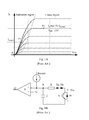
- FIG. 3B The increase of the voltage between the collector and the emitter of the upper switch S 41 achieved by reducing the driving voltage of the upper switch S 41 is illustrated by FIG. 3B .
- a plurality of solid curves are characteristic curves of the switch S 41 with respect to different gate voltages, and a dotted curve formed by grids is characteristic curve of the switch S 43 with respect to a 15V gate voltage (for clearness, only one characteristic curve of the switch S 43 is plotted).
- the switches S 41 and S 43 still have the characteristic curves of the corresponding switches S 1 and S 3 shown in FIG. 2H , and the rated current of the switch S 41 is greater than that of the switch S 43 .
- the voltage Vce between the collector and the emitter of the switch S 41 moves from the point P 11 in FIG. 2H to the point P 13 in FIG. 3B .
- the identification criterion of the static short current Isc is reduced, such that the voltage Vce between the collector and the emitter of the switch S 41 increases.
- the upper switch detecting unit X 41 in FIG. 3A can detect the occurrence of a short-circuit reliably.
- FIG. 3C is a schematic diagram illustrating the effect of detecting a short-circuit in the TNPC inverter performed the method illustrated in FIGS. 3A and 3B , wherein the manners of triggering a short circuit shown in FIG. 2D are adopted, CH 1 is the waveform of the voltage Vce (50V/div) between the collector and the emitter of the switch S 41 , CH 2 is the waveform of the driving voltage Vge_S 41 (5V/div) of the switch S 41 , CH 3 is the waveform of the driving voltage Vge_S 43 (5V/div) of the switch S 43 , and CH 4 is the experiment waveform of the short current Ic (1 kA/div) of the short-circuit path.
- the voltage Vce between the collector and the emitter of the switch S 41 is greater than 50V, such that the upper switch detecting unit X 41 in FIG. 3A can detect the occurrence of a short-circuit reliably.
- the TNPC inverter device may further include a driving voltage generating circuit.
- FIGS. 5A ⁇ 5 D illustrate examples of the driving voltage generating circuit with respect to the TNPC inverter device shown in FIG. 3A .
- the driving voltage generating circuit includes a driving voltage generating circuit for driving the upper switch S 41 (upper right in the drawing), which includes a stabilivolt D 51 .
- the driving voltage generating circuit further includes a driving voltage generating circuit for driving the first flow direction switch S 43 (lower right in the drawing), which includes a stabilivolt D 52 .
- the static driving voltages for driving the upper switch S 41 and for driving the first flow direction switch S 43 are substantially the same.
- the static driving voltage of the upper switch S 41 needs to be reduced to make the static driving voltage of the upper switch S 41 to be less than the static driving voltage of the first flow direction switch S 43 . As shown in FIG.
- auxiliary components such as diodes D 53 , D 54 , D 56 and D 57 , a stabilivolt D 55 , a switch S 51 , a transformer T, capacitors C 51 , C 52 , C 53 and C 54 , resistors R 51 and R 52 , and output lines such as nodes E 1 and E 3 , and connection terminals Vc 1 , Ve 1 , Vc 3 and Ve 3 , are further included in FIG. 5A , and the connection relationships among them are as shown in FIG. 5A , which are not repeated here.
- the static driving voltage of the upper switch S 41 being less than the static driving voltage of the first flow direction switch S 43 may also be, for example, achieved by adjusting voltage adjusting resistors in the driving voltage generating circuit.
- the driving voltage generating circuit for driving the upper switch S 41 includes voltage stabilizing integrated circuits IC 1 and IC 2 , and voltage adjusting resistors R 512 and R 522 .
- the driving voltage generating circuit for driving the first flow direction switch S 43 includes voltage stabilizing integrated circuits IC 3 and IC 4 , and voltage adjusting resistors R 532 and R 542 .
- the static driving voltage of the upper switch S 41 is less than the static driving voltage of the first flow direction switch S 43 .
- auxiliary components such as diodes D 531 , D 532 , D 541 , D 542 , D 56 and D 57 , a stabilivolt D 55 , a switch S 51 , a transformer T, capacitors C 51 , C 52 , C 53 and C 54 , resistors R 511 , R 521 , R 531 and R 541 , and output lines such as nodes E 1 and E 3 , and connection terminals Vc 1 , Ve 1 , Vc 3 and Ve 3 , are further included in FIG. 5 , and the connection relationships among them are as shown in FIG. 5B , which are not repeated here.
- the static driving voltage for driving the lower switch S 42 being less than the static driving voltage for driving the second flow direction switch S 44 may be achieved with reference to FIG. 5A or 5B .
- the driving voltage generating circuit may not be only formed by stabilivolts, or voltage stabilizing integrated circuits and voltage adjusting resistors, but also may be in other forms, or various combinations.
- the output of different static driving voltages may be achieved by adjusting parameters of corresponding components in the driving voltage generating circuit.
- the driving voltage generating circuit for driving the upper switch S 41 further includes a connection resistor Rg 1 , and when the static driving voltage of the upper switch S 41 is reduced, the switching loss of the upper switch S 41 may be reduced by decreasing the resistance of the connection resistor Rg 1 .
- FIG. 5C the driving voltage generating circuit for driving the upper switch S 41 further includes a connection resistor Rg 1 , and when the static driving voltage of the upper switch S 41 is reduced, the switching loss of the upper switch S 41 may be reduced by decreasing the resistance of the connection resistor Rg 1 .
- FIG. 5D is a schematic diagram illustrating that the driving voltage generating circuit for driving the first flow direction switch S 43 drives the first flow direction switch S 43 via a connection resistor Rg 3 , and the resistance of the connection resistor Rg 3 may not be decreased.
- the driving voltage generating circuit push-pull outputs via geminate switches Sin 1 and Sin 2 , pulse-width modulation signals PWM 1 and PWM 2 input via a resistor Rin, the upper switch S 41 and the first flow direction switch S 43 are respectively anti-parallelly connected with diodes D 41 and D 43 , nodes E 1 and E 3 shown in FIG. 5A are for example connected to nodes E 1 and E 3 shown in FIGS.
- connection terminals Vc 1 , Ve 1 , Vc 3 and Ve 3 are the same as those in FIGS. 5A and 5B , and the connection relationships among them are shown in FIGS. 5C and 5D , which are not repeated here.
- the same device or method may be adopted to reduce the switching loss, which is not repeated here.
- the parameters of the upper switch S 41 and the lower switch S 42 may be selected to be the same as or similar to those of the first flow direction switch S 43 and the second flow direction switch S 44 , thereby, the rated current of any one of the upper switch S 41 and the lower switch S 42 may not be greater than the rated current of any one of the first flow direction switch S 43 and the second flow direction switch S 44 .
- a plurality of solid curves are characteristic curves of the switch S 41 with respect to different gate voltages
- a dotted curve formed by grids is a characteristic curve of the switch S 43 with respect to a 15V gate voltage (for clearness, only one characteristic curve of the switch S 43 is plotted)
- a chain dotted curve formed by grids is another characteristic curve of the switch S 41 with 15V gate voltage under a circumstance that the rated current Irate_S 41 of the switch S 41 is less than the rated current Irate_S 43 of the switch S 43 (for clearness, only one characteristic curve of the switch S 41 is plotted).
- the static driving voltages of the switches S 41 and S 43 are the same, for example, the static driving voltage Vge_S 41 of the switch S 41 and the static driving voltage Vge_S 43 of the switch S 43 are kept to be 15V, then, by selecting parameters of the switches per se, the rated current Irate_S 41 of the switch S 41 decreases or the rated current Irate_S 43 of the switch S 43 increases, such that the rated current of the switch S 41 is less than the rated current Irate_S 43 of the switch S 43 .
- the voltage Vce between the collector and the emitter of the switch S 41 during the time when a short-circuit occurs operates at point P 14 not point P 11 in FIG. 3D , wherein the operating point P 11 is, for example, an intersection point on both the characteristic curve of the switch S 41 with normal rated current driving with 15V gate voltage, and the characteristic curve of the switch S 43 with smaller rated current compared with the rated current of the switch S 41 and driving with 15V gate voltage, and the operating point P 14 is an operating point on the characteristic curve of the switch S 41 with smaller rated current driving with 15V gate voltage.
- the identification criterion of the static short current Isc is reduced, such that a voltage Vce between the collector and the emitter of the switch S 41 increases, meanwhile a voltage Vce between the collector and the emitter of the switch S 43 does not increase, such that the bus voltage is mainly endured by the switch S 41 , and such that the upper switch detecting unit X 41 in FIG. 3A can detect the occurrence of a short circuit in the TNPC inverter sufficiently and reliably.
- a transconductance of the upper switch S 41 or the lower switch S 42 is less than a transconductance of the first flow direction switch S 43 or the second flow direction switch S 44 . In this way, the purpose for increasing the voltage Vce between the collectors and the emitters of the switch units S 41 or S 42 during a short circuit may be achieved.
- the short circuit path in the inverter shown in FIG. 2A is symmetric with that shown in FIG. 2C , thereby the above-mentioned solution may also be used to increase the voltage Vce between the collector and the emitter of the switch S 2 (i.e., corresponding to the switch unit S 42 in FIG. 3A ), so as to detect the occurrence of a short circuit. Therefore, detecting other short-circuit circumstances in TNPC by detecting the lower switch S 42 through the lower switch detecting unit X 42 are not repeated here.
- the short-circuit path shown in FIG. 2B only passes through the switches S 1 and S 2 (i.e., corresponding to the switches unit S 41 and S 42 in FIG. 3A ), but does not pass through the switches S 3 and S 4 , which can be exactly detected by the upper switch detecting unit and the lower switch detecting unit, thereby will not be repeated here.
- the above description is illustrated by taking the TNPC inverter module shown in FIG. 3A as an example, in which the short circuit detecting module mainly consisting of the upper switch detecting unit and the lower switch unit may achieve the detection of various paths of short circuit in the TNPC inverter modules.
- this kind of TNPC inverter module may efficiently reduce the number of switch detecting units used in the short circuit detecting module, and reduce the probability of false operation due to external interference to the switch detecting unit.
- the upper switch unit is not limited to the upper switch S 41
- the lower switch unit is not limited to the lower switch S 42
- the first flow direction switch unit is not limited to the first flow direction switch S 43 shown in FIG. 3A
- the second flow direction switch unit is not limited to the second flow direction switch S 44 shown in FIG. 3A .
- FIG. 4A is a schematic diagram illustrating an embodiment of an extended topology of the TNPC inverter device of the present application.
- the upper switch unit is formed of a plurality of switches S 411 , . . . and S 41 n connected in series
- the lower switch unit is formed of a plurality of switches S 421 , . . . and S 42 n connected in series.
- Such configuration of the upper and lower switch units is used for improving the operating voltage of the TNPC inverter module.
- FIG. 4B is a schematic diagram illustrating another embodiment of an extended topology of the TNPC inverter device of the present application. As shown in FIG.
- the upper switch unit may be formed of a plurality of switches S 411 , . . . and S 41 n connected in parallel
- the lower switch unit may be formed of a plurality of switches S 421 , . . . and S 42 n connected in parallel, so as to improve the operating current of the TNPC inverter module.
- FIG. 4C is a schematic diagram illustrating further another embodiment of an extended topology of the TNPC inverter device of the present application.
- the first flow direction switch unit may be formed of a plurality of switches S 431 , . . . and S 43 n connected in series
- the second flow direction switch unit may be formed of a plurality of switches S 441 , . . .
- FIG. 4D is a schematic diagram illustrating still another embodiment of an extended topology of the TNPC inverter device of the present application.
- the first flow direction switch unit may be formed of a plurality of switches S 431 , . . . and S 43 n connected in parallel
- the second flow direction switch unit may be formed of a plurality of switches S 441 , . . . and S 44 n connected in parallel, so as to improve the operating current of the TNPC inverter module.
- FIG. 4E is a schematic diagram illustrating an embodiment of a varied topology of the TNPC inverter device of the present application.
- the first flow direction switch unit and the second flow direction switch unit are connected in parallel, each of the switches constituting the first flow direction switch unit or the second flow direction switch unit is connected with a diode in reverse series, such as diodes D 43 and D 44 , and each of the switches constituting the upper switch unit or the lower switch unit is anti-parallelly connected with a diode.
- any switch in the upper switch unit and the lower switch unit is anti-parallelly connected with a diode, such as diodes D 41 , D 42 , D 441 , . . . and D 41 n , D 421 , . . . and D 42 n.
- a diode such as diodes D 41 , D 42 , D 441 , . . . and D 41 n , D 421 , . . . and D 42 n.
- the controllable switches include Insulated Gate Bipolar Transistor (IGBT), Metal-Oxide-Semiconductor Field-Effect Transistor (MOSFET), Bipolar Junction Transistor (BJT), Junction Field-Effect Transistor (JFET), Gate Turn-Off Thyristor (GTO) or Metal-Oxide-Semiconductor Control Transistor (MCT).
- IGBT Insulated Gate Bipolar Transistor
- MOSFET Metal-Oxide-Semiconductor Field-Effect Transistor
- BJT Bipolar Junction Transistor
- JFET Junction Field-Effect Transistor
- GTO Gate Turn-Off Thyristor
- MCT Metal-Oxide-Semiconductor Control Transistor
- a TNPC inverter module according to the present application for those of a TNPC three-level inverter module of a model F3L400R12PT4_B 26 (Infineon), in order to enable the short circuit detecting module to detect the short circuit in any path in the TNPC inverter module according to the present application, voltage drop of any one of the upper switch and the lower switch thereof when a short-circuit path is formed is greater than 5.6V.
- FIG. 6 is a schematic diagram illustrating a flow chart of the method for detecting a short circuit in a TNPC inverter device.
- the method for detecting occurrence of a short circuit in the TNPC inverter device which includes: a TNPC inverter module including a first DC terminal, a second DC terminal, an AC terminal, a capacitor bridge arm, an inverting bridge arm and a bi-directional switching bridge arm, wherein ends of the capacitor bridge arm and ends of the inverting bridge arm are correspondingly connected to the first DC terminal and the second DC terminal, ends of the bi-directional switching bridge arm are correspondingly connected to a midpoint of the capacitor bridge arm and a midpoint of the inverting bridge arm, the AC terminal is the midpoint of the inverting bridge arm, and the inverting bridge arm includes an upper switch unit and a lower switch unit.
- the TNPC inverter device further includes a short circuit detecting module mainly consisting of an upper switch detecting unit and a lower switch detecting unit, wherein the upper switch detecting unit is configured to detect a voltage drop of the upper switch unit, and the lower switch detecting unit is configured to detect a voltage drop of the lower switch unit.
- a short circuit detecting module mainly consisting of an upper switch detecting unit and a lower switch detecting unit, wherein the upper switch detecting unit is configured to detect a voltage drop of the upper switch unit, and the lower switch detecting unit is configured to detect a voltage drop of the lower switch unit.
- step S 101 only voltage drops of the upper switch unit and the lower switch unit in the TNPC inverter module are detected.
- step S 102 when any one of the voltage drops of the upper switch unit and the lower switch unit is greater than a reference value, it is determined that a path of a short circuit has been formed in the inverter.
- the detecting method may be applied to the above embodiments of various TNPC inverter module configurations, which are not repeated here.
- the methods for improving the voltage drop of the upper switch unit and the lower switch unit in the TNPC inverter module detected by the short circuit detecting module when a short-circuit occurs in the upper switch unit or the lower switch unit which are not repeated here.
- the TNPC inverter module may also be applied for rectification in other circumstances, which is not limited to the inverting function as limited by the name here.
- the present application performs a priority-ranked de-saturation to the switches in the inverting bridge arms of the TNPC inverter device, so that the voltage Vce between the collector and the emitter of the switch in the inverting bridge arm of the TNPC inverter device is increased, thereby only by detecting the voltage Vce between the collector and the emitter of the switch in the inverting bridge arm of the TNPC inverter device, the short-circuit in the TNPC inverter device may be detected reliably. Furthermore, since in the present disclosure, only the voltage Vce between the collector and the emitter of the switch in the inverting bridge arm of the TNPC inverter device is detected, the number of the detecting circuits is reduced, and thus the circuit is simple.
Landscapes
- Engineering & Computer Science (AREA)
- Power Engineering (AREA)
- Inverter Devices (AREA)
Applications Claiming Priority (3)
| Application Number | Priority Date | Filing Date | Title |
|---|---|---|---|
| CN201410251114.3 | 2014-06-06 | ||
| CN201410251114.3A CN105226975B (zh) | 2014-06-06 | 2014-06-06 | Tnpc逆变器装置及其桥臂短路检测方法 |
| CN201410251114 | 2014-06-06 |
Publications (2)
| Publication Number | Publication Date |
|---|---|
| US20150357935A1 US20150357935A1 (en) | 2015-12-10 |
| US9800176B2 true US9800176B2 (en) | 2017-10-24 |
Family
ID=53365870
Family Applications (1)
| Application Number | Title | Priority Date | Filing Date |
|---|---|---|---|
| US14/730,469 Active 2035-12-29 US9800176B2 (en) | 2014-06-06 | 2015-06-04 | TNPC inverter device and method for detecting short-circuit thereof |
Country Status (3)
| Country | Link |
|---|---|
| US (1) | US9800176B2 (de) |
| EP (1) | EP2953258B1 (de) |
| CN (1) | CN105226975B (de) |
Cited By (4)
| Publication number | Priority date | Publication date | Assignee | Title |
|---|---|---|---|---|
| US20180034386A1 (en) * | 2015-03-05 | 2018-02-01 | Sumitomo Electric Industries, Ltd. | Conversion device |
| US20180097515A1 (en) * | 2016-09-30 | 2018-04-05 | Infineon Technologies Austria Ag | System and Method for an Overpower Detector |
| US20190157987A1 (en) * | 2017-11-20 | 2019-05-23 | Solaredge Technologies, Ltd. | Efficient Switching for Converter Circuit |
| US12565111B1 (en) | 2025-03-05 | 2026-03-03 | dcbel Inc. | Bidirectional split-phase power converter for electric vehicle charging |
Families Citing this family (16)
| Publication number | Priority date | Publication date | Assignee | Title |
|---|---|---|---|---|
| DE102015104554A1 (de) * | 2014-05-16 | 2015-11-19 | Semikron Elektronik Gmbh & Co. Kg | Schaltungsanordnung |
| CN103986310B (zh) * | 2014-05-30 | 2017-07-14 | 台达电子企业管理(上海)有限公司 | 变流器电路及其开路检测方法 |
| US10205407B2 (en) * | 2015-09-16 | 2019-02-12 | sonnen GmbH | Inverter device, energy storage system and method of controlling an inverter device |
| US10263412B2 (en) * | 2016-12-22 | 2019-04-16 | Infineon Technologies Austria Ag | System and method for desaturation detection |
| TWI627828B (zh) * | 2017-03-13 | 2018-06-21 | 台達電子工業股份有限公司 | 電源轉換器與電源轉換方法 |
| CN106953326A (zh) * | 2017-05-04 | 2017-07-14 | 哈尔滨工业大学 | 一种适用于一类冲击性负载的混合谐波抑制技术 |
| CN109116207B (zh) * | 2018-06-20 | 2020-10-30 | 北京利德华福电气技术有限公司 | 预检测桥式结构中igbt异常的方法 |
| CN109655703B (zh) * | 2018-12-30 | 2022-01-28 | 北京天诚同创电气有限公司 | 并联功率模块的自检方法、装置、设备及存储介质 |
| CN110208606B (zh) * | 2019-06-03 | 2021-03-19 | 河北旭辉电气股份有限公司 | 一种svg装置直流支撑电容衰减情况的在线监测方法 |
| CN110401357A (zh) * | 2019-07-30 | 2019-11-01 | 江苏舾普泰克自动化科技有限公司 | 一种低损耗节能型船用逆变器 |
| CN110456198B (zh) * | 2019-08-14 | 2021-09-28 | 国网湖南省电力有限公司 | 链式svg两并一串测试模式下的软上电方法 |
| CN110794285B (zh) * | 2019-10-18 | 2021-06-22 | 淮安中科晶上智能网联研究院有限公司 | 一种全桥开关电路状态检测电路及方法 |
| CN113839576B (zh) * | 2021-08-06 | 2023-12-15 | 华为技术有限公司 | 驱动控制系统及方法 |
| CN116087826A (zh) * | 2022-12-22 | 2023-05-09 | 上能电气股份有限公司 | T型三电平逆变器桥臂的短路检测方法和电路 |
| WO2024189706A1 (ja) * | 2023-03-10 | 2024-09-19 | 三菱電機株式会社 | 半導体素子の駆動回路及び駆動装置 |
| CN119543682B (zh) * | 2024-09-30 | 2025-12-09 | 华为数字能源技术有限公司 | 功率变换器 |
Citations (10)
| Publication number | Priority date | Publication date | Assignee | Title |
|---|---|---|---|---|
| US5621628A (en) | 1995-06-13 | 1997-04-15 | Kabushiki Kaisha Toshiba | Power converter |
| US20110051478A1 (en) * | 2009-02-20 | 2011-03-03 | Toshiba Mitsubishi-Electric Indus. Sys. Corp. | Power conversion device |
| US20110242860A1 (en) * | 2010-04-06 | 2011-10-06 | Fuji Electric Holdings Co., Ltd. | Power semiconductor device and power conversion system using the device |
| US20120018777A1 (en) * | 2010-07-22 | 2012-01-26 | Fuji Electric Co., Ltd. | Three level power converting device |
| US20120161858A1 (en) | 2010-12-22 | 2012-06-28 | Converteam Technology Ltd. | Capacitor balancing circuit and control method for an electronic device such as a multilevel power inverter |
| CN102937688A (zh) | 2012-10-30 | 2013-02-20 | 浙江万里学院 | 二极管中点钳位三电平逆变器的器件开路故障诊断电路 |
| CN103312210A (zh) | 2013-03-08 | 2013-09-18 | 卧龙电气集团股份有限公司 | 一种三相四线制三电平光伏并网逆变器 |
| CN103368427A (zh) | 2012-04-05 | 2013-10-23 | 艾默生网络能源有限公司 | 单相逆变器及其系统和三相逆变器及其系统 |
| US20140247634A1 (en) * | 2011-10-06 | 2014-09-04 | Fuji Electric Co., Ltd. | Three-level power conversion circuit system |
| US20150003127A1 (en) * | 2013-06-26 | 2015-01-01 | Fuji Electric Co., Ltd. | Multilevel power conversion circuit |
-
2014
- 2014-06-06 CN CN201410251114.3A patent/CN105226975B/zh active Active
-
2015
- 2015-06-04 US US14/730,469 patent/US9800176B2/en active Active
- 2015-06-04 EP EP15170742.9A patent/EP2953258B1/de active Active
Patent Citations (10)
| Publication number | Priority date | Publication date | Assignee | Title |
|---|---|---|---|---|
| US5621628A (en) | 1995-06-13 | 1997-04-15 | Kabushiki Kaisha Toshiba | Power converter |
| US20110051478A1 (en) * | 2009-02-20 | 2011-03-03 | Toshiba Mitsubishi-Electric Indus. Sys. Corp. | Power conversion device |
| US20110242860A1 (en) * | 2010-04-06 | 2011-10-06 | Fuji Electric Holdings Co., Ltd. | Power semiconductor device and power conversion system using the device |
| US20120018777A1 (en) * | 2010-07-22 | 2012-01-26 | Fuji Electric Co., Ltd. | Three level power converting device |
| US20120161858A1 (en) | 2010-12-22 | 2012-06-28 | Converteam Technology Ltd. | Capacitor balancing circuit and control method for an electronic device such as a multilevel power inverter |
| US20140247634A1 (en) * | 2011-10-06 | 2014-09-04 | Fuji Electric Co., Ltd. | Three-level power conversion circuit system |
| CN103368427A (zh) | 2012-04-05 | 2013-10-23 | 艾默生网络能源有限公司 | 单相逆变器及其系统和三相逆变器及其系统 |
| CN102937688A (zh) | 2012-10-30 | 2013-02-20 | 浙江万里学院 | 二极管中点钳位三电平逆变器的器件开路故障诊断电路 |
| CN103312210A (zh) | 2013-03-08 | 2013-09-18 | 卧龙电气集团股份有限公司 | 一种三相四线制三电平光伏并网逆变器 |
| US20150003127A1 (en) * | 2013-06-26 | 2015-01-01 | Fuji Electric Co., Ltd. | Multilevel power conversion circuit |
Non-Patent Citations (5)
| Title |
|---|
| 1st OA dated May 4, 2017 by the CN Office. |
| Arlt, Bodo, "Electronics in Motion and Conversion", Bodo's Power Systems, ISSN: 1863-5598, ZKZ 64717 05-12, May 2012, pp. 1-103. |
| Device application Technology Dept., Fuji Electric co.,Ltd., "Evaluation Driver Board for AT-NPC 3-level 4in1 IGBT module", Fuji Electric Innovationg Energy Technology, Application Note-PRELIMINARY, AN-125, ver1.0, Dec. 2013, pp. 1-23. |
| European search report dated Jan. 5, 2016 from corresponding No. EP 15170742.9. |
| Siani, Alain, "AN2012-03 F3L2020E07-F-P EVAL Evaluation Driver Board for EconoPACK TM 4 3-Level Modules in NPC2-Topology with 1ED020112-B2 gate driver IC" , Application Note AN 2012-03, V1.1, Feb. 2014, pp. 1-19. |
Cited By (7)
| Publication number | Priority date | Publication date | Assignee | Title |
|---|---|---|---|---|
| US20180034386A1 (en) * | 2015-03-05 | 2018-02-01 | Sumitomo Electric Industries, Ltd. | Conversion device |
| US10644614B2 (en) * | 2015-03-05 | 2020-05-05 | Sumitomo Electric Industries, Ltd. | Conversion device having a control unit for detecting arm short-circuit |
| US20180097515A1 (en) * | 2016-09-30 | 2018-04-05 | Infineon Technologies Austria Ag | System and Method for an Overpower Detector |
| US10868529B2 (en) * | 2016-09-30 | 2020-12-15 | Infineon Technologies Austria Ag | System and method for an overpower detector |
| US20190157987A1 (en) * | 2017-11-20 | 2019-05-23 | Solaredge Technologies, Ltd. | Efficient Switching for Converter Circuit |
| US10536094B2 (en) * | 2017-11-20 | 2020-01-14 | Solaredge Technologies Ltd. | Efficient switching for converter circuit |
| US12565111B1 (en) | 2025-03-05 | 2026-03-03 | dcbel Inc. | Bidirectional split-phase power converter for electric vehicle charging |
Also Published As
| Publication number | Publication date |
|---|---|
| CN105226975A (zh) | 2016-01-06 |
| CN105226975B (zh) | 2017-12-15 |
| EP2953258B1 (de) | 2020-12-23 |
| EP2953258A3 (de) | 2016-01-27 |
| US20150357935A1 (en) | 2015-12-10 |
| EP2953258A2 (de) | 2015-12-09 |
Similar Documents
| Publication | Publication Date | Title |
|---|---|---|
| US9800176B2 (en) | TNPC inverter device and method for detecting short-circuit thereof | |
| US10224920B2 (en) | Soft shutdown modular circuitry for power semiconductor switches | |
| US11139808B2 (en) | Semiconductor device and power conversion system | |
| US11356013B2 (en) | Method of short-circuiting a faulty converter submodule and power converter supporting same | |
| US8823354B2 (en) | Power semiconductor switch series circuit and control method thereof | |
| US7570086B2 (en) | Switching element drive circuit | |
| KR101571952B1 (ko) | 스위칭 회로 및 반도체 모듈 | |
| US20190386483A1 (en) | Igbt short-circuit detection and protection circuit and igbt-based controllable rectifier circuit | |
| JP3447949B2 (ja) | 絶縁ゲート型半導体素子のゲート駆動回路、電力変換装置 | |
| US20200186140A1 (en) | Control circuit and power conversion device | |
| CN101253675A (zh) | 带有分布式储能器的变流电路 | |
| JP2009506736A (ja) | 分散配置されたエネルギー蓄積器を有する電力変換回路 | |
| US10727729B2 (en) | Power converter | |
| CN107765160B (zh) | 一种igbt器件的测试电路及测试方法 | |
| EP3539215B1 (de) | Schaltung von parallelem, rückwärts leitendem igbt und schalter mit grosser bandbreite | |
| US20160006368A1 (en) | Power Converter | |
| Bayerer | Parasitic inductance hindering utilization of power devices | |
| US20210135662A1 (en) | A protection arrangement for an mmc-hvdc sub-module | |
| US20160231358A1 (en) | Semiconductor device | |
| WO2023140083A1 (ja) | 電力変換装置 | |
| US11394200B2 (en) | Device and method for coupling two DC grids | |
| US9923482B2 (en) | System and method for a power inverter with controllable clamps | |
| KR102778232B1 (ko) | 직접 직렬연결 가능한 모듈, 컨버터 체인, 컨버터 및 제어 방법 | |
| CN111869068A (zh) | 开关装置以及开关装置的控制方法 | |
| KR101542940B1 (ko) | 멀티 레벨 컨버터의 사고 전류 저감 구조 및 이를 이용한 장치 |
Legal Events
| Date | Code | Title | Description |
|---|---|---|---|
| AS | Assignment |
Owner name: DELTA ELECTRONICS (SHANGHAI) CO., LTD., CHINA Free format text: ASSIGNMENT OF ASSIGNORS INTEREST;ASSIGNORS:DING, XIBING;FENG, WEIYI;ZHANG, WEIQIANG;AND OTHERS;REEL/FRAME:035785/0895 Effective date: 20140709 |
|
| STCF | Information on status: patent grant |
Free format text: PATENTED CASE |
|
| MAFP | Maintenance fee payment |
Free format text: PAYMENT OF MAINTENANCE FEE, 4TH YEAR, LARGE ENTITY (ORIGINAL EVENT CODE: M1551); ENTITY STATUS OF PATENT OWNER: LARGE ENTITY Year of fee payment: 4 |
|
| MAFP | Maintenance fee payment |
Free format text: PAYMENT OF MAINTENANCE FEE, 8TH YEAR, LARGE ENTITY (ORIGINAL EVENT CODE: M1552); ENTITY STATUS OF PATENT OWNER: LARGE ENTITY Year of fee payment: 8 |