US9867272B2 - Generation and acceleration of charged particles using compact devices and systems - Google Patents
Generation and acceleration of charged particles using compact devices and systems Download PDFInfo
- Publication number
- US9867272B2 US9867272B2 US14/436,859 US201314436859A US9867272B2 US 9867272 B2 US9867272 B2 US 9867272B2 US 201314436859 A US201314436859 A US 201314436859A US 9867272 B2 US9867272 B2 US 9867272B2
- Authority
- US
- United States
- Prior art keywords
- electrode segments
- charged particles
- linear series
- resonator
- voltage
- Prior art date
- Legal status (The legal status is an assumption and is not a legal conclusion. Google has not performed a legal analysis and makes no representation as to the accuracy of the status listed.)
- Expired - Fee Related, expires
Links
Images


Classifications
-
- H—ELECTRICITY
- H05—ELECTRIC TECHNIQUES NOT OTHERWISE PROVIDED FOR
- H05H—PLASMA TECHNIQUE; PRODUCTION OF ACCELERATED ELECTRICALLY-CHARGED PARTICLES OR OF NEUTRONS; PRODUCTION OR ACCELERATION OF NEUTRAL MOLECULAR OR ATOMIC BEAMS
- H05H9/00—Linear accelerators
- H05H9/04—Standing-wave linear accelerators
- H05H9/041—Hadron LINACS
- H05H9/045—Radio frequency quadrupoles
-
- H—ELECTRICITY
- H01—ELECTRIC ELEMENTS
- H01J—ELECTRIC DISCHARGE TUBES OR DISCHARGE LAMPS
- H01J37/00—Discharge tubes with provision for introducing objects or material to be exposed to the discharge, e.g. for the purpose of examination or processing thereof
- H01J37/02—Details
- H01J37/04—Arrangements of electrodes and associated parts for generating or controlling the discharge, e.g. electron-optical arrangement or ion-optical arrangement
- H01J37/06—Electron sources; Electron guns
-
- H—ELECTRICITY
- H01—ELECTRIC ELEMENTS
- H01J—ELECTRIC DISCHARGE TUBES OR DISCHARGE LAMPS
- H01J37/00—Discharge tubes with provision for introducing objects or material to be exposed to the discharge, e.g. for the purpose of examination or processing thereof
- H01J37/02—Details
- H01J37/04—Arrangements of electrodes and associated parts for generating or controlling the discharge, e.g. electron-optical arrangement or ion-optical arrangement
- H01J37/147—Arrangements for directing or deflecting the discharge along a desired path
- H01J37/1472—Deflecting along given lines
-
- H—ELECTRICITY
- H05—ELECTRIC TECHNIQUES NOT OTHERWISE PROVIDED FOR
- H05H—PLASMA TECHNIQUE; PRODUCTION OF ACCELERATED ELECTRICALLY-CHARGED PARTICLES OR OF NEUTRONS; PRODUCTION OR ACCELERATION OF NEUTRAL MOLECULAR OR ATOMIC BEAMS
- H05H7/00—Details of devices of the types covered by groups H05H9/00, H05H11/00, H05H13/00
- H05H7/04—Magnet systems, e.g. undulators, wigglers; Energisation thereof
-
- H—ELECTRICITY
- H05—ELECTRIC TECHNIQUES NOT OTHERWISE PROVIDED FOR
- H05H—PLASMA TECHNIQUE; PRODUCTION OF ACCELERATED ELECTRICALLY-CHARGED PARTICLES OR OF NEUTRONS; PRODUCTION OR ACCELERATION OF NEUTRAL MOLECULAR OR ATOMIC BEAMS
- H05H9/00—Linear accelerators
- H05H9/04—Standing-wave linear accelerators
- H05H9/041—Hadron LINACS
- H05H9/042—Drift tube LINACS
-
- H—ELECTRICITY
- H01—ELECTRIC ELEMENTS
- H01J—ELECTRIC DISCHARGE TUBES OR DISCHARGE LAMPS
- H01J2237/00—Discharge tubes exposing object to beam, e.g. for analysis treatment, etching, imaging
- H01J2237/06—Sources
- H01J2237/063—Electron sources
-
- H—ELECTRICITY
- H01—ELECTRIC ELEMENTS
- H01J—ELECTRIC DISCHARGE TUBES OR DISCHARGE LAMPS
- H01J2237/00—Discharge tubes exposing object to beam, e.g. for analysis treatment, etching, imaging
- H01J2237/15—Means for deflecting or directing discharge
-
- H—ELECTRICITY
- H05—ELECTRIC TECHNIQUES NOT OTHERWISE PROVIDED FOR
- H05H—PLASMA TECHNIQUE; PRODUCTION OF ACCELERATED ELECTRICALLY-CHARGED PARTICLES OR OF NEUTRONS; PRODUCTION OR ACCELERATION OF NEUTRAL MOLECULAR OR ATOMIC BEAMS
- H05H7/00—Details of devices of the types covered by groups H05H9/00, H05H11/00, H05H13/00
- H05H7/04—Magnet systems, e.g. undulators, wigglers; Energisation thereof
- H05H2007/043—Magnet systems, e.g. undulators, wigglers; Energisation thereof for beam focusing
-
- H—ELECTRICITY
- H05—ELECTRIC TECHNIQUES NOT OTHERWISE PROVIDED FOR
- H05H—PLASMA TECHNIQUE; PRODUCTION OF ACCELERATED ELECTRICALLY-CHARGED PARTICLES OR OF NEUTRONS; PRODUCTION OR ACCELERATION OF NEUTRAL MOLECULAR OR ATOMIC BEAMS
- H05H7/00—Details of devices of the types covered by groups H05H9/00, H05H11/00, H05H13/00
- H05H7/04—Magnet systems, e.g. undulators, wigglers; Energisation thereof
- H05H2007/046—Magnet systems, e.g. undulators, wigglers; Energisation thereof for beam deflection
Definitions
- This patent document relates to generation of charged particle pulses such as electron pulses and uses of such charged particle pulses in various applications, including terahertz-wave generation and time-resolved microscopy.
- This patent document relates to linear charged particle accelerators which accelerate charged particles to have desired particle energy or speed for various applications.
- This patent document provides techniques, devices and systems that generate short charged particle packets or pulses of charged particles, e.g., electron packets. Certain implementations of the disclosed technology may be configured to achieve one or more advantages or benefits, including, e.g., providing charged particle generators without requiring a fast-switching-laser source.
- a device for generating charged particle packets or pulses includes a charged particle deflector for receiving a stream of continuous charged particles propagating along a first direction.
- the charged particle deflector is operable to deflect the stream of continuous charged particles to a set of directions different from the first direction.
- the device also includes a series of beam blockers located downstream from the charged particle deflector and spaced from one another in a periodic or with spacing designed for appropriate timing, linear or slightly angled configuration as a series of impediments for the electron beam to propagate.
- This array of beam blockers can interact with the deflected stream of charged particles and divide the stream of the charged particles into a set of short particle packets.
- the charged particles are electrons.
- the duration of the short particle packets is of sub-picosecond.
- the charged particle deflector can be configured with a ramp voltage applied across the pair of electrodes, wherein the ramp voltage causes the continuous electron beam passing through the charged particle deflector to sweep across the array of beam blockers.
- a system for generating charged particle packets or pulses includes a charged particle source that produces a stream of continuous charged particles to propagate along a charged particle path.
- the system also includes a charged particle deflector positioned in the charged particle path to deflect the stream of continuous charged particles to a set of directions different from the charged particle path.
- the system additionally includes a series of beam blockers located downstream from the charged particle deflector and spaced from one another in a linear configuration as a beam-blocker grating. This beam-blocker grating can interact with the deflected stream of charged particles and divide the stream of the charged particles into a set of short particle packets.
- the charged particles are electrons.
- the duration of the short particle packets is of sub-picosecond to a few femtoseconds.
- the beam blockers are conductors.
- the charged particle deflector can be configured with a ramp voltage applied across the pair of electrodes, wherein the ramp voltage causes the continuous electron beam passing through the charged particle deflector to sweep across the array of beam blockers.
- a compact linear charged particle accelerator for accelerating charged particles.
- This compact LINAC includes a radio frequency (RF) signal generator for generating an RF signal.
- the compact LINAC also includes an RF resonator coupled to the RF signal generator and operable to generate a high-voltage RF drive signal based on the received RF signal.
- the compact LINAC further includes a linear series of electrode segments coupled to the RF resonator and configured to pass and accelerate charged particles successively through a channel of the linear series of electrode segments, wherein each electrode segment of the linear series of electrode segments is driven by the high-voltage RF drive signal.
- the RF resonator is implemented as a coplanar waveguide.
- a co-planar linear charged particle accelerator to include a planar platform; and coplanar waveguide resonators formed on the planar platform as RF cavities to achieve high voltages at a particle path defined by the coplanar waveguide resonators for accelerating charged particles.
- the coplanar waveguide resonators formed on the planar platform may include multiple layers of coplanar waveguide resonators.
- the planar platform may include a printed circuit board and wire bonds that are electrically coupled to the coplanar waveguide resonators.
- FIG. 1 illustrates a block-diagram of an exemplary device for generating charged particle packets or pulses in accordance with some embodiments described herein.
- FIG. 2 illustrates a schematic of an exemplary device for generating short electron packets by implementing a knife-edge sampling technique in the charged particle grating of device 100 in accordance with some embodiments described herein.
- FIG. 3 illustrates an electron-packet generation process by sweeping a continuous electron beam across a deflector module and a grating module in accordance with some embodiments described herein.
- FIG. 4 illustrates a schematic of the electron-packet generating device 200 and the operation principle of the proposed knife-edge sampling technique for generating short electron packets from a long-duration or continuous electron beam in accordance with some embodiments described herein.
- FIG. 5 shows plots of t 2 , t 3 , u y (t 2 ) and D as a function of the time of injection into the deflector electrodes, t 1 based on Eq. 13a, Eq. 8, and Eq. 11 in accordance with some embodiments described herein.
- FIG. 6 shows a plot of the horizontal distance (D) traveled by an electron inside the drift region before exiting as a function of the time at which the exit occurs (t 3 ) in accordance with some embodiments described herein.
- FIG. 7 shows a plot of horizontal sweep velocity V swp along the boundary of the drift region as a function of the time of exit t 3 in accordance with some embodiments described herein.
- FIG. 8 shows a picture of the experimental setup for the single slit experiment in accordance with some embodiments described herein.
- FIG. 9 shows plots of the deflector (scaled) and the detector voltage recorded simultaneously through an oscilloscope when the deflector electrodes were driven by a 400V signal at a repetition rate of 125 Hz by a pulser circuit in accordance with some embodiments described herein.
- FIG. 10 shows a picture of the experimental setup inside the vacuum chamber for the multiple-slit grating experiment in accordance with some embodiments described herein.
- FIG. 11 shows the plot of measured current through a transimpedance amplifier with 1M ⁇ gain connected to an oscilloscope.
- FIG. 12 shows the electron trajectories as simulated by a commercial ELM and particle tracing software (OperaTM) in accordance with some embodiments described herein.
- FIG. 13A illustrates a schematic of an exemplary compact coplanar-waveguide-resonator LINAC (CPWR LINAC) for accelerating charged particles in accordance with some embodiments described herein.
- CPWR LINAC compact coplanar-waveguide-resonator LINAC
- FIG. 13B presents simulation results of an exemplary CPWR LINAC design (Simion) in accordance with some embodiments described herein.
- FIG. 13C shows particle beam focusing operation using V Einzel biased electrode segments in accordance with some embodiments described herein.
- FIG. 13D shows a block diagram of DC focusing voltage (V Einzel ) generating circuit in accordance with some embodiments described herein
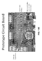
- FIG. 13E shows a photo of a circuit board which implements the DC focusing voltage generating circuit of FIG. 13D in accordance with some embodiments described herein.
- FIG. 13F illustrates using the disclosed CPWR LINACs to focus multiple electron beams (e-beams) in the application of e-beam lithography on a photoresist (PR)-covered wafer in accordance with some embodiments described herein.
- FIG. 14 shows two perspective views of a CPWR LINAC comprising a folded RF resonator designed as a coplanar waveguide integrated with electrode segments in accordance with some embodiments described herein.
- FIG. 15 illustrates using the described fabrication process to fabricate an on-chip Einzel lens in accordance with some embodiments described herein.
- FIG. 16 shows the experiment setup, which includes an electron gun, the CPWR LINAC, external power-supplies in accordance with some embodiments described herein.
- FIG. 17 illustrates a more detailed experiment setup in accordance with some embodiments described herein.
- FIG. 18 shows Amptek CdTe diode detector calibration result in accordance with some embodiments described herein.
- FIG. 19 shows the measured Bremsstrahlung curve with a beam current of 1 ⁇ A in accordance with some embodiments described herein.
- Table 1 presents listing of parameters used in the analytical calculations of the base case study in accordance with some embodiments described herein.
- Table 2 presents a parameter summary of multiple and single slit experiments in accordance with some embodiments described herein.
- This patent document provides techniques, devices and systems that generate short charged particle packets or pulses (e.g., electron packets) without expensive ultrafast lasers and disclosed implementations can be used to provide a knife-edge sampling technique by using linear arrays of beam blockers, such as conductor gratings to generate electron packets with short packet durations, e.g., on the order of femtoseconds to picoseconds.
- beam blockers such as conductor gratings
- the energy or speed of the charged particles may need increased by using linear charged particle accelerators.
- LINAC LINear particle ACcelerator
- Synchrotron Synchrotron
- Cyclotron Cyclotron
- many of the existing particle accelerators are heavy and bulky by using permanent magnets, power supplies, and cooling systems to generate high electromagnetic fields to accelerate particles.
- Charged particle acceleration could also be achieved with the use of pyro-electric crystals to produce an accelerating field. Although this method could potentially realize small sized devices, the crystals must be heated and is limited in the amount of field produced, and hence limited acceleration.
- Wake fields induced by femto-second lasers have also been shown to produce intense accelerating electric fields in plasma.
- the size and power consumption of the wake fields system cannot be easily reduced.
- LINAC is a type of oscillating field accelerator, which uses alternating high electric fields to accelerate the particles along a straight line. Typically, the higher the energy of the particle is accelerated to, the longer the length of the LINAC is required. In fact the famous high energy LINAC at SLAC National Accelerator Laboratory is 3.2 km long. LINACs with lower energy targets have also been produced, but these LINACs are disadvantaged because of their larger size compared to other low-energy-target accelerators.
- the LINAC designs in this patent document can be implemented by using RF resonators that, at certain resonant frequencies, enhance the voltage oscillation intensity with a gain proportional to the quality factor (Q-factor) of the resonator.
- Q-factor quality factor
- the traditional LINAC design without the present RF resonator designs usually produces a peak voltage around 70V.
- the RF resonator designs in this document with a large Q e.g., 100
- the disclosed technology can be used to construct coplanar waveguide resonators as RF cavities to achieve high voltages.
- the coplanar waveguides enable low-profile accelerators comparable to the height of silicon-cascaded accelerators structures. Such accelerators can be cascaded on top of each other for high density charged particle manipulation. Such designs can be implemented by configuring the LINAC and RF resonator in planar technology and thus can be integrated easily with other electronics. In addition, certain fabrication processes or techniques involved in such planar technology, e.g. PCB patterning and Si microsculpting, are well characterized and developed.
- Ultrafast lasers with femtosecond pulse durations can be used to generate short electron packets. Such ultrafast lasers tend to be expensive, may suffer performance issues and usually require complex maintenance.
- This patent document provides examples of techniques, devices and systems that generate short charged particle packets or pulses (e.g., electron packets) without using ultra-fast lasers.
- the disclosed technology can be used to enable cost effective, compact size electron pulse generators for applications such as terahertz-wave generation, time-resolved microscopy, cathodoluminescence, and e-beam lithography.
- one exemplary generator for generating charged particle packets or pulses includes a charged particle source that produces a stream of charged particles to propagate along a charged particle path; a charged particle deflector in the charged particle path to deflect the charged particles; and a series of conductors located downstream from the charged particle deflector and spaced from one another in a linear configuration as a conductor grating along the charged particle path to interact with the deflected charged particles to divide the stream of the charged particles into short particle packets.
- Another exemplary generator for generating coherent electromagnetic pulses of charged particles includes a charged particle source that produces a stream of charged particles to propagate along a charged particle path; and a series of beam blockers spaced from one another in a linear configuration (such as a periodic configuration) as a conductor grating along the electron path to interact the stream of electrons to induce electrical currents on the conductors to cause electromagnetic radiation pulses from the induced electrical currents on the conductors, wherein the conductors are arranged in a way that far fields of electromagnetic radiation from the conductors are coherently added to form a coherent electromagnetic pulse.
- FIG. 1 illustrates a block-diagram of an exemplary device 100 for generating charged particle packets or pulses in accordance with some embodiments described herein.
- device 100 comprise a charged particle source 102 that produces a stream of charged particles 104 which propagates along a charged particle path.
- a charged particle deflector 106 of device 100 is positioned in the charged particle path to deflect the stream of charged particles 104 and outputs a stream of deflected charged particles 108 .
- Device 100 further includes a charged particle grating 110 positioned along the charged particle path and downstream from charged particle deflector 106 .
- Charged particle grating 110 interacts with the stream of deflected charged particles 108 and divides the stream of the charged particles 108 into short charged particle packets 112 as the output of charged particle grating 110 .
- charged particle grating 110 comprises a series of beam blockers located and spaced from one another in a linear configuration as an orifice array.
- the series of beam blockers is arranged in a direction which is substantially along the charged particle path.
- the orifice array is placed in the same direction as the beam, creating a much faster sweep velocity across the orifices than if the orifices, as a small sweep angle leads to a wide sweep across the array.
- the series of beam blockers is a set of conductors.
- FIG. 2 illustrates a schematic of an exemplary device 200 for generating short electron packets by implementing a knife-edge sampling technique in the charged particle grating 110 of device 100 in accordance with some embodiments described herein.
- the exemplary device includes three modules: an electron source module 202 which corresponds to charged particle source 102 in device 100 , an electrostatic deflector module 206 which corresponds to charged particle deflector 106 in device 100 , and a grating module 210 which corresponds to charged particle grating 110 in device 100 .
- grating module 210 forms a drift region for the charged particles.
- device 200 and exemplary systems and techniques hereinafter are described in the context of the electrons, the present invention can generally be used for any type of charged particles (either negatively charged or positively charged), not just electrons.
- electron source module 202 can produce a continuous-wave (CW) or a long-duration electron packet 204 that is introduced to the downstream electrostatic deflector module 206 .
- electrostatic deflector module 206 comprises two parallel plate electrodes with a ramp voltage V p applied across the two electrodes. The ramped deflector voltage V p causes the continuous electron beam passing through deflector module 206 to sweep across a grating module 210 .
- electrostatic deflector module 206 may also include a first-level static-voltage deflector stage positioned before the ramp-voltage deflector stage, so that charged particles pass through both the static-voltage deflector stage and the ramp-voltage deflector stage.
- grating module 210 comprises a series of pillars/barriers 212 located downstream from deflector module 206 and spaced from one another in a periodic linear configuration.
- the series of pillars/barriers 212 forms a “grating” of alternating apertures/slits and pillars/barriers.
- the series of pillars/barriers 212 is made of electrically conductive material, i.e., conductors.
- each of the series of pillars/barriers can be of a rectangular cuboid shape, but can also be of cylinder, trapezoidal prism or other shapes.
- the grid-like boundary acts like multiple knife-edges that divides the incoming electron beam into short length electron packets 208 .
- the duration of the short packets 208 and the distance between the packets may be based on the voltage ramp rate and also the grating configurations, and more details are provided below.
- the apertures/slits in the grid-like boundary are very narrow in the direction of the electron beam sweeping to cause short duration electron bunches to be generated through such small aperture dimensions.
- the system parameters are arranged in such a way that the electron packets cause a coherent Smith-Purcell radiation as they pass over the grating.
- grating module 210 shown in FIG. 2 includes multiple apertures/slits, other embodiments of the grating module can include a single aperture/slit.
- the series of pillars/barriers 212 is arranged along a direction 214 which is substantially parallel to, or at a small angle with respect to the initial undeflected electron beam trajectory 216 .
- the deflected electron beam can reach any of the pillars/barriers 212 in a much shorter time in comparison to the cases when the undeflected electron beam trajectory 216 form a larger angle with respect to direction 214 . Consequently, the configuration of device 200 facilitates reducing the duration between successive electrode packets produced by grating module 210 .
- the inset in FIG. 2 also provides a side-view of grating module 210 . As can be seen in the inset, grating module 210 comprises an array of alternating pillars and slits.
- FIG. 3 illustrates an electron-packet generation process by sweeping a continuous electron beam across deflector module 306 and grating module 310 in accordance with some embodiments described herein.
- grating module 310 is formed by a first set of pillars/barriers 312 and a second set of pillars/barriers 314 opposing the first set of pillars/barriers 312 .
- all the pillars/barriers 312 and pillars/barriers 314 are conductors and all are connected to the same potential, e.g., the ground.
- the region/space between pillars/barriers 312 and pillars/barriers 314 is electromagnetically shielded and is referred to as the “drift region” for the electrons entering the space.
- FIG. 3 shows that all the pillars in a set of pillars 312 or 314 are arranged along the x-direction, other embodiments can have the pillars arranged at an angle with respect to the x-direction, as indicated by the set of dashed-line boxes over the set of pillars/barriers 312 .
- the electrons pass through the deflecting region between deflector module 206 , they experience an electric field (in the y-direction) perpendicular to their initial velocity (in the x-direction), thereby attaining a transverse velocity component that sweeps them across one or more pillar boundaries.
- the pillars will stop the beam and act like shutters to produce packets of electrons.
- the duration of the electron packets and charge density may be determined by the width and length of the deflector module 206 , the deflector ramp voltage V p , and the dimension of the pillars, among other parameters. Note that the electron packets emanating the grating travel in different directions.
- a set of electrodes may be positioned outside of the grating module 310 in the paths of the emanated electron packets to correct the initial paths so that these electron packets travel substantially in the same direction.
- ramp voltage V p can be repeated at a desired repetition rate for generating a periodic source of charged-particle-packets trains.
- the following sections provide analysis of electron dynamics in an electron packet generator which uses the knife-edge sampling technique based on the exemplary electron-packet generating device 200 .
- FIG. 4 illustrates a schematic of electron-packet generating device 200 and the operation principle of the proposed knife-edge sampling technique for generating short electron packets from a long-duration or continuous electron beam in accordance with some embodiments described herein.
- a continuous beam or a long packet of electrons with initial x-velocity, V x , and kinetic energy, KE i is assumed to enter into the gap between the deflector electrodes at time t 1 .
- These electrons travel through an electrostatic deflector region 402 formed by a parallel plate electrode pair driven by ramp voltage V p . While the electrons without any deflector voltage typically travel straight through the drift region, electrons that are subjected to the ramp voltage in deflector region 402 obtain a vertical velocity component through deflector region 402 .
- the successive drift region 404 formed by two opposing sets of conductors all coupled to the ground, electrons which move along a linear trajectory either are stopped by the pillars/barriers located at one set of positions in the boundary of the drift region or exit through openings located at the other set of positions in the boundary of the drift region. Moreover, the voltage ramp causes the electrons to sweep across the boundary, which results in the modulation of the initially continuous beam causing short electron packets to emanate from the drift region.
- the spatial and temporal distribution of the election packets are dictated by multiple parameters including, but are not limited to the length of the deflector, gap between the deflector plates, pillar/grid spacing, and initial electron energy KE i , and horizontal sweep velocity of electrons across the grid-like boundary of the drift region.
- the deflector region 402 and drift region 404 are configured such that the initial undeflected electron beam trajectory is substantially parallel to the center line of drift region 404 , i.e., the direction of periodic linear configuration of the grating.
- the electron dynamics in this exemplary implementation may be understood by the following analysis.
- the time spent by the electrons in the deflector region is associated with the length of the deflector region divided by the initial horizontal velocity V x .
- V x is assumed to be constant due to lack of horizontally acting forces.
- the gap between the deflector electrodes is labeled as g, and the electrons enter the deflector near the center of the gap, with initial separation of g/2 from either electrode.
- the inset in FIG. 4 plots a transient waveform of an exemplary ramp function V p (t) and also shows the times t 1 , t 2 , and t 3 at which the given electrode enters the deflector region, exits the deflector region, and exits the drift region, respectively.
- the transverse acceleration a y of the electron in the above time interval can be calculated as:
- m 0,e denotes the rest mass of an electron
- ⁇ (m/s 3 ) is defined as:
- u y ⁇ ( t 2 ) ⁇ ( t 2 3 - t 1 2 ⁇ ( 3 ⁇ t 2 - 2 ⁇ t 1 ) 6 ) . ( 8 )
- t 1 as a function of the drift region exit length, D, we can use Eq. 1, Eq. 10, Eq. 11, and Eq. 12 to solve t 1 , t 2 , and t 3 as follows:
- An important objective in the design of the electron-packet generator is to minimize the duration between successive electron packets coming out of the grid-like boundary of the drift region. Note that this duration can depend on the shape and orientation of the knife-shaped pillars in the grating, which can vary in angle, width, and location. Although the analysis in conjunction with FIG. 4 assumes that the pillars are parallel to the direction of the beam for its simplicity, different configurations of the pillars in their angle, width, and location can be used in the proposed device.
- duration of the electron packets also varies as a function of the point of emanation
- duration may be approximated by the ratio of the distance between two adjacent pillars to the horizontal sweep velocity, V swp , of the beam over the pillars/slits at the point of emanation. Consequently, computation of V swp of the electrons across this boundary is needed.
- V swp the horizontal sweep velocity
- V swp V x ⁇ ⁇ ⁇ t , crash ⁇ t 3 .
- ⁇ ⁇ 2 V swp ( 21 )
- ⁇ 2 the pitch length between the pillars as shown in FIG. 4 . Since the sweep velocity will typically be larger for electrons with larger V x , Eq. 21 implies that, as we increase the initial kinetic energy of the electrons, the duration between the ejected pulses will decrease. Moreover, decreasing the gap and pillar pitch distance will also reduce the duration between the electron packets.
- FIG. 5 shows plots of t 2 , t 3 , u y (t 2 ) and D as a function of the time of injection into the deflector electrodes, t 1 based on Eq. 13a, Eq.
- the distance travelled by the charged particles decreases as a function of the injection time, t 1 , because the particle experiences higher voltage regions of the ramp function in the deflector region.
- t 3 has a minima as a function of t 1 , indicating the time at which the first particles hit the boundary of the drift region, either being obstructed by a pillar or emanating off this region.
- the electron-packet generator shown in FIG. 4 can be operated as a last-in-first-out system.
- the electrons that enter into the deflector region later i.e., t 1 relatively large
- exit before the electrons that entered into the deflector region at earlier times i.e., t 1 relatively small.
- FIG. 6 shows a plot of the horizontal distance (D) traveled by an electron inside the drift region before exiting as a function of the time at which the exit occurs (t 3 ) in accordance with some embodiments described herein.
- the inset shows the zoomed in version of the distance (D) traveled by an electron inside the drift region before exiting, as a function of the time at which the exit occurs (t 3 ), 0.8 ns ⁇ t 3 ⁇ 1.2 ns.
- D the distance traveled by an electron inside the drift region before exiting
- first-in-first-out characteristic zoomed in the inset distance (D) traveled by an electron inside the drift tube decreases for electrons emanating the drift region at a later time.
- distance (D) traveled by an electron inside the drift tube increases for electrons emanating the drift region at a later time.
- First-in-last-out or first-in-first-out regions can also be identified from the slope of the t 3 vs t 1 curve shown in FIG. 5 .
- FIG. 7 shows a plot of horizontal sweep velocity V swp along the boundary of the drift region as a function of the time of exit t 3 in accordance with some embodiments described herein. Note that both the numerical derivative of the curve in FIG. 6 and the analytical calculation based on Eq. 20 are plotted in FIG. 7 , and a good match between the two approaches can be observed.
- the computed values of V swp in FIG. 7 includes both positive and negative sweep velocities.
- the electron-packet generator in conjunction with FIGS. 2-4 can be configured as a last-in-first-out system as described above, in some embodiments, the electron-packet generators in this disclosure can be configured as first-in-first-out systems, such that the electrons that enter into the deflector region earlier (i.e., t 1 relatively small), exit before the electrons that entered into the deflector region at later times (i.e., t 1 relatively large). This can be achieved by adjusting geometrical parameters of the embodiment or properly selected ramp voltage V p (t) applied across the deflector electrodes, among other things.
- an electron-pulse generating device (or a “pulse-generating device”) was designed and fabricated by laser-cutting FR4 PC-boards with a commercially available instrument, LPKF ProtoLaser U. Custom laser micromachining recipes have been developed to pattern and cut thick FR-4 PC-boards and silicon substrates at a resolution of 100-200 ⁇ m with wall roughness of 10 ⁇ m. After laser cutting, the pieces were assembled to realize high aspect ratio 3D structures.
- a Kimball Physics EMG-4212 electron gun was used at a pressure of 10 ⁇ 5 Torr.
- the beam initial electron energy was 2 keV for the multiple pillar experiment and 5 keV for the single slit experiment.
- alignment of the device was important to the experiment.
- the beam which had a diameter of 1 mm, has to pass through the cover hole of the deflector and make a parallel trajectory towards the deflector plates. In order to achieve precise alignment.
- a BeO plate was used to locate the position of the beam prior to installing the pulse-generating device. Once the location of the beam was confirmed by observing the light on the BeO disk, the actual pillar and the detector were then installed.
- FIG. 8 shows a picture of the experimental setup for the single slit experiment in accordance with some embodiments described herein.
- the electron beam passes through the deflector 800 and is swept across a single slit 802 located at the top of the picture.
- the width of the single slit 802 is 1.5 mm and the injected electrons have an energy of 5 keV.
- the pillars in the grating shown in FIG. 8 are placed at an angle to the initial undeflected beam trajectory 804 .
- FIG. 9 plots the deflector 800 (scaled) and the detector 806 voltage recorded simultaneously through an oscilloscope when the deflector electrodes were driven by a 400V signal at a repetition rate of 125 Hz by a pulser circuit in accordance with some embodiments described herein. More specifically, the top plot in FIG. 9 represents the attenuated deflector 800 voltage and the bottom plot represents the detector 806 voltage. The rise and fall of the deflector voltage corresponds to a unique dip in the detector output. The energy of the electrons used for this experiment was 5 keV, the width of the slit was 1.5 mm, and the distance of the deflector to the slit was 7 cm.
- the deflector voltage As the deflector voltage is increased to its maximum value, the electron beam sweeps across the single slit, and this is detected as a ⁇ 1.5 V peak on the detector through an oscilloscope with a low-frequency input impedance of 1M ⁇ . After reaching its maximum value, the deflector voltage drops again to ground, producing another negative peak on the detector plate. Note that each rise and fall of the deflector voltage results in a negative peak in the detector output, yielding the expected frequency doubling effect.
- FIG. 10 shows a picture of the experimental setup inside the vacuum chamber for the multiple-slit grating 1002 experiment in accordance with some embodiments described herein.
- the electron is injected from the bottom of the picture along an initial undeflected beam trajectory 1004 towards the top of the picture through the hole of the deflector 1000 .
- 2 keV electrons are used instead of 5 keV electrons used in the first set of experiments.
- Pillar plate with 12 gratings was tested as a knife-edge device to examine the current change on the detector plate.
- the deflector 1000 voltage is driven by a DC source instead of a pulser.
- the electron beam is initially blocked by the grounded pillar wall.
- the deflector voltage is turned on and increased from 0 V to 480 V in steps of 10 V, the electron beam sweeps across the grid plate. This causes the modulation of the electron current incident on the detector 1006 behind multiple-slit grating 1002 . This current is measured through a transimpedance amplifier with 1M ⁇ gain connected to an oscilloscope and is plotted in FIG. 11 .
- the top schematic in FIG. 11 represents the experimental setup.
- the bottom graph in FIG. 11 shows the current ( ⁇ A) of the detector 1006 as the deflector 1000 voltage is increased from 0 V to 480 V.
- the current ranged from 0.1 ⁇ A to 1.4 ⁇ A with increasing peak to peak excursions as the deflector voltage is increased.
- FIG. 12 shows the electron trajectories as simulated by a commercial FEM and particle tracing software (OperaTM) in accordance with some embodiments described herein.
- Two cases of static deflector voltage are presented that result in electron incidence on the multiple-slit grating at different positions.
- the bottom two pictures show beam tracing simulation results of the multiple-slit experiments at low (left) and high (right) deflector voltages.
- Experimental data is also included on the top of the figure to highlight this association. Due to the configuration of the pillars in the multiple-slit grating, some of the beam passes through the pillar for low deflector voltages, but is blocked fully at larger deflector voltages.
- FIG. 12 highlights this fact by showing mappings between electron trajectories and the low/high-voltage ranges of the data of FIG. 11 .
- the minimum pulse duration observed may be limited by the bandwidth of the amplifier connected to the detector. Improvement of the amplifier bandwidth and positioning the preamplifier inside the vacuum chamber will enable detection of shorter pulse durations.
- a focused beam size is another important factor in generating short pulses.
- a chip-level Einzel lens can be incorporated before the deflector region to reduce the beam size and obtain a shorter pulse duration.
- an electron energy of 174.9 keV can be generated in electron packets by using a deflector gap of 1 mm, and a deflector voltage ramp rate of 1000 V/ns to achieve electron pulse durations shorter than 1 ps for a pillar pitch of 200 ⁇ m.
- Implementations of a sub-picosecond electron pulse generator can be achieved without requiring a fast-switching-laser source. It is found that the minimum time duration between electron packets may be limited by the energy of the incoming continuous electron beam.
- a fast ramping high voltage supply can be used to minimize overall system dimensions, including the drift region through which electrons travel at constant velocity. Slow voltage ramps can also provide short pulses if there is sufficient flexibility on the length of the drift region.
- a linear particle accelerator is to accelerate a beam of charged particles by passing the particles through a linear series of electrode segments, each separated from each other by a small gap.
- the tubes are driven at radio frequency (RF) with each tube segment oscillating ⁇ out of phase with respect to the adjacent tube.
- RF radio frequency
- This setup is designed such that the particle will arrive at the gaps between the tubes exactly when the potential difference between the 2 tubes is the highest, hence pushing the particle in the direction of motion to achieve the desired acceleration.
- the energy (i.e., speed) of the particle increases, the length that it traverses in a period of RF oscillation increases, hence the lengths of the segments consecutively increase accordingly.
- Some embodiments described herein provide compact LINAC designs which can generate 10-1000 keV electrons with 1-50 ⁇ A beam current.
- the proposed compact LINACs employs coplanar waveguide resonators as RF cavities to achieve high voltages.
- the coplanar waveguides enable low-profile accelerators comparable to the height of silicon wafer thickness, compatible with silicon-cascaded accelerators structures. Such accelerators can be cascaded on top of each other for high density charged particle manipulation.
- some disclosed compact LINAC implementations provide an all integrated electric-field-only accelerator without energy inefficient, bulky equipment in other LINAC designs.
- the proposed compact RF LINAC provides RF resonators that, at certain resonant frequencies, enhance the voltage oscillation intensity with a gain proportional to the quality factor (Q-factor) of the resonators.
- Q-factor quality factor
- the input peak-peak voltage oscillation is 70V for an input power of 50 W
- the peak voltage without the resonator is at most 70V.
- the Q-factor being on the order of 100
- the resulting voltage intensity can potentially be around 7000V.
- some proposed LINACs and the associated RF resonator are constructed with planar technology which can be easily integrated with other electronics.
- FIG. 13A illustrates a schematic of an exemplary CPWR LINAC 1300 for accelerating charged particles in accordance with some embodiments described herein.
- the CPWR LINAC 1300 includes an RF signal generator 1302 for generating an RF oscillation signal, an amplifier 1304 coupled to RF signal generator 1302 and operable to amplify the RF oscillation signal, and a linear series of electrode segments 1306 for accelerating charged particles.
- CPWR LINAC 1300 also includes an RF resonator 1308 which is coupled between the output of amplifier 1304 and electrode segments 1306 , and operable to multiply the amplitude of the received RF oscillation signal by a large factor as a result of the resonant effect.
- the high peak-peak RF output from RF resonator 1308 is coupled to electrode segments 1306 through a set of wire bonds 1310 to provide the required drive signals.
- wire bonds 1310 shown in FIG. 13A can replace wire bonds 1310 shown in FIG. 13A with other electrical coupling techniques to deliver drive signals to electrode segments 1306 , such as using planar conductor wires or planar waveguides.
- each electrode segment in electrode segments 1306 comprises a pair of parallel electrode blocks, and the gap between the pair of electrode blocks forms the path or “channel” for the charged particles to traverse.
- different electrode segments have different lengths as required by the traditional drift tube theory. Hence, the charged particles will traverse electrode segments 1306 through the channel formed between the two linear row of electrode blocks. Note that a set of gaps 1312 is formed between different electrode segments.
- electrode segments 1306 are driven by RF drive signals configured such that each electrode segment is driven ⁇ out of phase with respect to the adjacent electrode segment.
- This setup is designed such that the particle will arrive at the gaps 1312 between the electrode segments exactly when the potential difference between the 2 electrode segments is the highest, hence pushing the particle in the direction of movement to achieve the desired acceleration.
- FIG. 13B presents simulation results of an exemplary CPWR LINAC design (Simion) in accordance with some embodiments described herein.
- the top graph in the figure shows that phases of the RF drive signal at different locations along the series of electrode segments. Note that the phase difference near the gaps of the electrode segments is the largest.
- the bottom graph in the figure shows the particle energy as a function of travel distance.
- the flat regions in the plot correspond to the movements within the electrode segments, whereas the “jumps” in energy correspond to the acceleration as the particle crosses the gaps between the electrode segments.
- the charged particles will enter electrode segments 1306 from the left hand side of electrode segments 1306 and exit from the right hand side of electrode segments 1306 after acceleration.
- the high-energy charged particles exiting electrode segments 1306 can enter a charged particle storage 1314 located on the right hand side of electrode segments 1306 and be temporarily stored for later use.
- RF resonator 1308 is constructed as a coplanar waveguide (CPW) using printed circuit board (PCB) technology.
- PCB printed circuit board
- RF resonator 1308 can be implemented with different patterns and configurations, such as the linear pattern shown in FIG. 13A , or the meander pattern shown in FIGS. 14 and 17 .
- Different waveguide configurations such as stripline, or floating back-electrode are possible to achieve different resonator configurations.
- both RF resonator 1308 and electrode segments 1306 can be micro-fabricated and can have compact sizes, they can be integrated on the same PCB-board to form a compact unit, thereby allowing a compact CPWR LINAC design.
- both RF resonator 1308 and the linear series of electrode segments 1306 are formed on the same surface.
- FIG. 13A illustrates one example design for implementing the CPWR LINAC design, other configurations may also be possible.
- micro-fabricated CPW RF resonators, such as RF resonator 1308 can be used together with tradition drift tubes instead of compact electrode segments 1306 , which can still achieve certain size reduction in a LINAC design.
- electrode segments 1306 are driven by RF signals for charged particle acceleration.
- electrode segments 1306 can be used as Einzel lens when biased with specific DC voltages (i.e., V Einzel ) for focusing charged particle beam as they travel through electrode segments 1306 .
- FIG. 13C shows particle beam focusing operation using V Einzel biased electrode segments 1306 in accordance with some embodiments described herein.
- Subplot (b) shows various geometrical configurations of the electrode segments (A/D) under constant V Einzel and corresponding beam focusing effects.
- Subplot (c) shows cascaded Einzel lens configurations of the electrode segments under the same V Einzel and the same total lengths of the electrode segments, and the corresponding beam focusing effects.
- FIG. 13D shows a block diagram of DC focusing voltage (V Einzel ) generating circuit in accordance with some embodiments described herein.
- FIG. 13E shows a photo of a circuit board which implements the DC focusing voltage generating circuit of FIG. 13D in accordance with some embodiments described herein.
- the above-described DC focusing voltage (V Einzel ) generating circuit can be integrated with RF amplifier 1304 and RF resonator 1308 in FIG. 13A on the same PCB-board.
- CPWR LINAC 1300 can be configured with dual functions of both charged particle (e.g., electrons) acceleration and for charged particle beam (e.g., electron beam) focusing.
- the electrodes can be configured for other beam shaping components such as electrostatic quadrupoles for modifying beam cross-sections.
- FIG. 13F illustrates using the disclosed CPWR LINACs to focus multiple electron beams (e-beams) in the application of e-beam lithography on a PR-covered wafer in accordance with some embodiments described herein. Note that in the embodiment shown, an array of electrode blocks can be shared by two linear series of electrode blocks.
- some embodiments can use a combined RF and DC drive signal to drive either the proposed LINAC device or the proposed Einzel lens (i.e., a superposition of a DC signal and an RF signal using a bias tee for instance).
- coplanar waveguides in an CPWR LINACs can be formed on FR4 PCB-boards, Rogers material, or sapphire, among other techniques, to facilitate planar RF signal propagation.
- planar films on planar substrates can be used to obtain microstrip, stripline, and coplanar wire structures in CPWR LINACs.
- the quality factor of the proposed CPW resonators can be as high as 500 at frequencies up to 10 GHz, enabling high electric fields in such resonators. This field may be limited by the breakdown of the various dielectrics, which is ⁇ 30 kV/mm for materials like Rogers 4000 series.
- CPWR LINAC To test the CPWR LINAC, charged particles such as electrons of known energy are injected into the CPWR LINAC, where the coplanar waveguide driven electrode segments accelerate the charged particles. The X-rays generated as a result of Bremsstrahlung radiation from the accelerated particles can then be measured with a detector (e.g., a CdTe detector) for energy analysis.
- a detector e.g., a CdTe detector
- a CPWR LINAC is designed for input electron energy of 5 keV in consideration of the minimum energy resolution threshold of the Amptek X-ray detector used in the experiments.
- the length of the first electrode segment in the linear series of electrode segments may be chosen to accommodate an initial injection energy of 5 keV.
- the length of the subsequent electrode segments can be computed. For example, assuming the acceleration is 100 eV in each stage, the length of the fifth electrode segment is determined to be 2.08 cm.
- the gaps between the electrode segments are chosen to be 1 mm. Note that if the quality factor of the resonator is increased, the electric field in the gaps will increase, and the acceleration will be greater than 100 eV. As a result, the length of the consecutive electrode segments would need to be increased.
- phase focusing Another important design factor of the CPWR LINAC is the phase focusing. As the number of stages increases in the LINAC, some of the particles will no longer match the phase of the oscillating electric potential. Phase match between the accelerated particles and the RF field is often crucial in transferring energy to the particles along different stages of electrode segments.
- a simple method to maintain the phase focusing is to drive the accelerating particles at a slightly smaller phase than the phase that would yield maximum energy. This will slow down the velocity of the particles that are faster than the nominal velocity (i.e., the designed value) and accelerate particles that are travelling at a slower speed.
- an optimal RF frequency for the device operation can be determined from the length of the electrode segments. For example, RF frequency of 1.04 GHz is computed to match the oscillation of the electric field to the transit time of the electrons as:
- FIG. 14 shows two perspective views of a CPWR LINAC 1400 comprising a folded RF resonator designed as a coplanar waveguide 1402 integrated with electrode segments 1404 in accordance with some embodiments described herein.
- a CPWR LINAC 1400 comprising a folded RF resonator designed as a coplanar waveguide 1402 integrated with electrode segments 1404 in accordance with some embodiments described herein.
- four different acceleration stages are use within a total length of 10 cm.
- four layers of silicon are stacked together and bonded using vacuum compatible conducting epoxy yielding a total height of 2 mm.
- the coplanar waveguide 1402 is built on a FR4 PCB-board.
- the electromagnetic field integrity and cross coupling considerations of the coplanar waveguide can make shorter electrode segments less desirable.
- the electrode segments 1404 are raised above the coplanar waveguide 142 to minimize the electric field between the ground of the coplanar waveguide and the electric potential of the electrode segments.
- the series of electrode segments 1306 in LINAC 1300 can be fabricated using the following process.
- a commercially available laser micromachining tool (LPKF ProtoLaser U) is used for patterning electrodes and etching deep channels in four different silicon wafers. These wafers are then stacked and adhesively formed. The laser is then used to break the tethers that were included in the design to ensure alignment between the four layers and the PCB.
- FIG. 15 illustrates using the described fabrication process to fabricate a single stage of electrode segments 1306 in accordance with some embodiments described herein. As illustrated in FIG. 15 , a 4 ⁇ m of oxide is deposited on the top side and photoresist (PR) layer is spun on the bottom side of the wafer in step (a).
- PR photoresist
- step (d) silicon is cut by laser in step (b).
- PR layer is then stripped and aluminum is sputtered to realize conductive surfaces in step (c).
- step (d) the whole assembly is stacked on the PCB-board using posts, and the silicon/Al electrodes are wire-bonded to copper pads in step (d).
- the inset in FIG. 15 shows a more detailed cross-sectional view of the multiple-layer electrode segment.
- the channel between the two silicon/Al stacks is where the charged particles are contained.
- the multiple-layer stack creates a greater height of the channel which allows a better charged particle confinement within the electrode segment.
- different silicon layers are coupled to separate wire bonds, thereby allowing them to receive independent drive signals.
- DRIE Deep Reactive Ion Etching
- FIG. 16 shows the experiment setup, which includes an electron gun, the CPWR LINAC, external power-supplies in accordance with some embodiments described herein.
- an RF signal generator (Agilent N9310A) is used to provide the oscillating field, which is connected to the RF power amplifier (Ophir 5205) for power amplification.
- the amplified signal is fed to the coplanar waveguide within LINAC through the bidirectional coupler (Agilent 778D).
- the electron beam from the electron gun (Kimball Physics EMG-4212) is slightly tilted at an angle from the center, which requires alignment prior to the experiment.
- FIG. 17 illustrates a more detailed experiment setup in accordance with some embodiments described herein. More specifically, the left figure in FIG. 17 represents alignment with the phosphorous screen, while the right figure shows the alignment process where a laser is shined through the LINAC system.
- Simple copper electrode patterns defined on a PCB were used for electron detection using a current-meter (Keithley 2400). Two of these PCB detectors, which had their front copper isolated into four segments with a hole in the middle to let the electron beam pass through, were used. A deviation of the electron beam from the center would generate current in one of the four electrodes, which is detected by the current-meter.
- These 4-segmented PCB detectors were integrated into the LINAC device at the electron entrance and exit to ensure beam trajectory alignments which are shown in FIG. 17 as PCB detectors 1702 .
- the LINAC is installed inside the chamber for testing. 5 keV electrons are injected through the channel of the LINAC at a beam current of 1 ⁇ A. The particles accelerate as they pass through the four stages of the LINAC and collide with the copper plate to generate X-rays due to Bremsstrahlung radiation.
- Amptek CdTe diode detector is used to analyze the X-rays generated from the LINAC. Prior to the LINAC experiment, the X-ray detector was calibrated using a known source of Cd-109.
- FIG. 18 shows Amptek CdTe diode detector calibration result in accordance with some embodiments described herein.
- the x-axis of the resulting graph from the X-ray detector is given as a number of channels, which represents the energy to be calibrated.
- the y-axis of the graph is the number of counts which is the quantity of the X-ray emission.
- One of the Cd-109 K ⁇ emissions is expected to have energy of 22 keV.
- the detector was tested with the electron gun.
- the energy of the electrons impinging on the copper plate was incremented from 4 keV to 7 keV in steps of 1 keV with a beam current of 1 ⁇ A.
- the Bremsstrahlung curve from the X-rays was observed to shift to the right as expected for higher energies.
- the peak of the 5 keV occurred at 2.8 keV, which also confirms the calibration made using Cd-109.
- FIG. 19 shows the measured Bremsstrahlung curve with a beam current of 1 ⁇ A in accordance with some embodiments described herein. It can be seen that the difference between the two Bremsstrahlung peaks is 21. Using the calibration factor, this channel difference can be converted to an energy difference of 0.37 keV.
- a compact coplanar-waveguide-based LINAC were disclosed and its preliminary operation demonstrated.
- the fabricated compact LINAC system showed an acceleration of 0.37 keV for a 5 keV electron beam at a beam current of 1 ⁇ A.
- Further acceleration in the proposed LINAC structure can be obtained by feeding higher power through impedance matching between the power source and the coplanar waveguide of the resonator.
- developing a custom X-band oscillator, RF amplifier, and integrating those at the PCB level with the coplanar waveguide can further reduce the size of the LINAC and will enable a LINAC system in the 10-cc scale.
Landscapes
- Physics & Mathematics (AREA)
- Engineering & Computer Science (AREA)
- Plasma & Fusion (AREA)
- Spectroscopy & Molecular Physics (AREA)
- Chemical & Material Sciences (AREA)
- Analytical Chemistry (AREA)
- Optics & Photonics (AREA)
- Particle Accelerators (AREA)
- Lasers (AREA)
Priority Applications (1)
| Application Number | Priority Date | Filing Date | Title |
|---|---|---|---|
| US14/436,859 US9867272B2 (en) | 2012-10-17 | 2013-10-17 | Generation and acceleration of charged particles using compact devices and systems |
Applications Claiming Priority (4)
| Application Number | Priority Date | Filing Date | Title |
|---|---|---|---|
| US201261715144P | 2012-10-17 | 2012-10-17 | |
| US201261715225P | 2012-10-17 | 2012-10-17 | |
| PCT/US2013/065549 WO2014123591A2 (fr) | 2012-10-17 | 2013-10-17 | Génération et accélération de particules chargées à l'aide de systèmes et de dispositifs compacts |
| US14/436,859 US9867272B2 (en) | 2012-10-17 | 2013-10-17 | Generation and acceleration of charged particles using compact devices and systems |
Related Parent Applications (1)
| Application Number | Title | Priority Date | Filing Date |
|---|---|---|---|
| PCT/US2013/065549 A-371-Of-International WO2014123591A2 (fr) | 2012-10-17 | 2013-10-17 | Génération et accélération de particules chargées à l'aide de systèmes et de dispositifs compacts |
Related Child Applications (1)
| Application Number | Title | Priority Date | Filing Date |
|---|---|---|---|
| US15/865,056 Continuation US10440810B2 (en) | 2012-10-17 | 2018-01-08 | Generation and acceleration of charged particles using compact devices and systems |
Publications (2)
| Publication Number | Publication Date |
|---|---|
| US20160174355A1 US20160174355A1 (en) | 2016-06-16 |
| US9867272B2 true US9867272B2 (en) | 2018-01-09 |
Family
ID=51300233
Family Applications (2)
| Application Number | Title | Priority Date | Filing Date |
|---|---|---|---|
| US14/436,859 Expired - Fee Related US9867272B2 (en) | 2012-10-17 | 2013-10-17 | Generation and acceleration of charged particles using compact devices and systems |
| US15/865,056 Active US10440810B2 (en) | 2012-10-17 | 2018-01-08 | Generation and acceleration of charged particles using compact devices and systems |
Family Applications After (1)
| Application Number | Title | Priority Date | Filing Date |
|---|---|---|---|
| US15/865,056 Active US10440810B2 (en) | 2012-10-17 | 2018-01-08 | Generation and acceleration of charged particles using compact devices and systems |
Country Status (2)
| Country | Link |
|---|---|
| US (2) | US9867272B2 (fr) |
| WO (1) | WO2014123591A2 (fr) |
Cited By (4)
| Publication number | Priority date | Publication date | Assignee | Title |
|---|---|---|---|---|
| US20180343734A1 (en) * | 2012-10-17 | 2018-11-29 | Cornell University | Generation and acceleration of charged particles using compact devices and systems |
| US10367508B1 (en) * | 2018-05-18 | 2019-07-30 | Varex Imaging Corporation | Configurable linear accelerator trigger distribution system and method |
| US11570881B2 (en) * | 2018-01-29 | 2023-01-31 | Hitachi, Ltd. | Circular accelerator, particle therapy system with circular accelerator, and method of operating circular accelerator |
| US12245356B2 (en) * | 2019-12-19 | 2025-03-04 | Elekta Limited | Radiotherapy device |
Families Citing this family (11)
| Publication number | Priority date | Publication date | Assignee | Title |
|---|---|---|---|---|
| EP3133633B1 (fr) * | 2016-02-24 | 2018-03-28 | FEI Company | Étude du comportement dynamique d'un échantillon dans un microscope à particules chargées |
| WO2017192834A1 (fr) * | 2016-05-04 | 2017-11-09 | Cornell University | Accélérateur de particules chargées à base de tranche, composants de tranche, procédés et applications |
| KR20180090494A (ko) | 2017-02-03 | 2018-08-13 | 삼성전자주식회사 | 기판 구조체 제조 방법 |
| JP7244814B2 (ja) * | 2018-04-09 | 2023-03-23 | 東芝エネルギーシステムズ株式会社 | 加速器の制御方法、加速器の制御装置、及び粒子線治療システム |
| CN109661860A (zh) * | 2018-11-26 | 2019-04-19 | 新瑞阳光粒子医疗装备(无锡)有限公司 | 粒子加速器及其引出粒子能量的确定方法、装置和介质 |
| DE102020119875B4 (de) * | 2020-07-28 | 2024-06-27 | Technische Universität Darmstadt, Körperschaft des öffentlichen Rechts | Vorrichtung und Verfahren zum Führen geladener Teilchen |
| US11476087B2 (en) * | 2020-08-03 | 2022-10-18 | Applied Materials, Inc. | Ion implantation system and linear accelerator having novel accelerator stage configuration |
| US11596051B2 (en) * | 2020-12-01 | 2023-02-28 | Applied Materials, Inc. | Resonator, linear accelerator configuration and ion implantation system having toroidal resonator |
| EP4388823A4 (fr) * | 2021-08-17 | 2025-06-25 | Omega-P R&D, Inc. | Accélérateur de haute puissance à résonance cyclotron compact pour électrons |
| US11825590B2 (en) * | 2021-09-13 | 2023-11-21 | Applied Materials, Inc. | Drift tube, apparatus and ion implanter having variable focus electrode in linear accelerator |
| CN114867182B (zh) * | 2022-01-14 | 2024-07-30 | 天津大学 | 一种用于带电粒子储存的紧凑型静电储存环装置 |
Citations (30)
| Publication number | Priority date | Publication date | Assignee | Title |
|---|---|---|---|---|
| US5311566A (en) * | 1992-09-22 | 1994-05-10 | The Titan Corporation | In-situ x-ray treatment of organically contaminated material |
| US5401973A (en) * | 1992-12-04 | 1995-03-28 | Atomic Energy Of Canada Limited | Industrial material processing electron linear accelerator |
| US5744919A (en) * | 1996-12-12 | 1998-04-28 | Mishin; Andrey V. | CW particle accelerator with low particle injection velocity |
| US5814940A (en) * | 1995-04-12 | 1998-09-29 | Denki Kogyo Co., Ltd. | Radio frequency particle accelerator having means for synchronizing the particle beam |
| US5994708A (en) * | 1996-09-25 | 1999-11-30 | Nikon Corporation | Demagnifying charged-particle lithography apparatus |
| US6060833A (en) * | 1996-10-18 | 2000-05-09 | Velazco; Jose E. | Continuous rotating-wave electron beam accelerator |
| US6320334B1 (en) * | 2000-03-27 | 2001-11-20 | Applied Materials, Inc. | Controller for a linear accelerator |
| US6326746B1 (en) * | 1999-06-23 | 2001-12-04 | Advanced Ion Beam Technology, Inc. | High efficiency resonator for linear accelerator |
| US20040126072A1 (en) * | 2001-08-02 | 2004-07-01 | Hoon Lee Howard Wing | Optical devices with engineered nonlinear nanocomposite materials |
| US7005669B1 (en) * | 2001-08-02 | 2006-02-28 | Ultradots, Inc. | Quantum dots, nanocomposite materials with quantum dots, devices with quantum dots, and related fabrication methods |
| US20060255268A1 (en) * | 2003-03-24 | 2006-11-16 | Juergen Frosien | Charged particle beam device with detection unit switch and method of operation thereof |
| US20070138980A1 (en) * | 2005-11-14 | 2007-06-21 | The Regents Of The University Of California | Cast dielectric composite linear accelerator |
| US7259373B2 (en) * | 2005-07-08 | 2007-08-21 | Nexgensemi Holdings Corporation | Apparatus and method for controlled particle beam manufacturing |
| US20080219297A1 (en) * | 2005-09-12 | 2008-09-11 | Hironari Yamada | Linear x-ray laser generator |
| US7426067B1 (en) * | 2001-12-17 | 2008-09-16 | Regents Of The University Of Colorado | Atomic layer deposition on micro-mechanical devices |
| US20080258653A1 (en) * | 2007-04-17 | 2008-10-23 | Advanced Biomarker Technologies, Llc | Cyclotron having permanent magnets |
| US7541905B2 (en) * | 2006-01-19 | 2009-06-02 | Massachusetts Institute Of Technology | High-field superconducting synchrocyclotron |
| US7553686B2 (en) * | 2002-12-17 | 2009-06-30 | The Regents Of The University Of Colorado, A Body Corporate | Al2O3 atomic layer deposition to enhance the deposition of hydrophobic or hydrophilic coatings on micro-electromechanical devices |
| US7576499B2 (en) * | 2004-01-15 | 2009-08-18 | Lawrence Livermore National Security, Llc | Sequentially pulsed traveling wave accelerator |
| US20090218520A1 (en) * | 2006-05-26 | 2009-09-03 | Advanced Biomarker Technologies, Llc | Low-Volume Biomarker Generator |
| US20090224700A1 (en) * | 2004-01-15 | 2009-09-10 | Yu-Jiuan Chen | Beam Transport System and Method for Linear Accelerators |
| US7656258B1 (en) * | 2006-01-19 | 2010-02-02 | Massachusetts Institute Of Technology | Magnet structure for particle acceleration |
| US20100032580A1 (en) * | 2006-10-24 | 2010-02-11 | Lawrence Livermore National Security, Llc | Compact Accelerator For Medical Therapy |
| US20120235603A1 (en) * | 2009-10-02 | 2012-09-20 | Oliver Heid | Accelerator and method for actuating an accelerator |
| US20130106316A1 (en) * | 2011-10-31 | 2013-05-02 | Lawrence Livermore National Security, Llc | Resistive foil edge grading for accelerator and other high voltage structures |
| US20130140468A1 (en) * | 2011-12-05 | 2013-06-06 | Lawrence Livermore National Security, Llc | Charged particle beam scanning using deformed high gradient insulator |
| US8598813B2 (en) * | 2012-01-17 | 2013-12-03 | Compact Particle Acceleration Corporation | High voltage RF opto-electric multiplier for charge particle accelerations |
| US20140049193A1 (en) * | 2012-08-15 | 2014-02-20 | Transmute, Inc. | Accelerator Having Acceleration Channels Formed Between Covalently Bonded Chips |
| US8927950B2 (en) * | 2012-09-28 | 2015-01-06 | Mevion Medical Systems, Inc. | Focusing a particle beam |
| US9301384B2 (en) * | 2012-09-28 | 2016-03-29 | Mevion Medical Systems, Inc. | Adjusting energy of a particle beam |
Family Cites Families (10)
| Publication number | Priority date | Publication date | Assignee | Title |
|---|---|---|---|---|
| US9205463B2 (en) * | 2005-09-26 | 2015-12-08 | Lawrence Livermore National Security, Llc | Isotope specific arbitrary material sorter |
| US7994472B2 (en) * | 2008-06-16 | 2011-08-09 | The Board Of Trustees Of The Leland Stanford Junior University | Laser-driven deflection arrangements and methods involving charged particle beams |
| EP2340148A4 (fr) * | 2008-09-09 | 2012-05-02 | Univ Cornell | Grille optique pour un procédé haute précision et haute résolution de nanofabrication à l échelle d'une tranche |
| WO2010065702A2 (fr) * | 2008-12-05 | 2010-06-10 | Cornell University | Accélérateur de particules guidées par champ électrique, procédé et applications |
| US20110026033A1 (en) * | 2008-12-19 | 2011-02-03 | Metroalaser, Inc. | Optical Inspection Using Spatial Light Modulation |
| DE102010010716A1 (de) * | 2010-03-08 | 2012-02-16 | Bernhard Hidding | Verfahren zum Testen der Empfindlichkeit elektronischer Bauteile durch Teilchen- und Photonenstrahlen mittels Laser-Plasma-Wechselwirkung |
| US9867272B2 (en) * | 2012-10-17 | 2018-01-09 | Cornell University | Generation and acceleration of charged particles using compact devices and systems |
| EP2964003A4 (fr) * | 2013-02-28 | 2016-10-05 | Mitsubishi Electric Corp | Procédé de fabrication d'un accélérateur haute fréquence, accélérateur haute fréquence, et système d'accélérateur circulaire |
| JP6086819B2 (ja) * | 2013-05-29 | 2017-03-01 | 住友重機械イオンテクノロジー株式会社 | 高エネルギーイオン注入装置 |
| US10342108B2 (en) * | 2015-08-12 | 2019-07-02 | Asml Netherlands B.V. | Metrology methods, radiation source, metrology apparatus and device manufacturing method |
-
2013
- 2013-10-17 US US14/436,859 patent/US9867272B2/en not_active Expired - Fee Related
- 2013-10-17 WO PCT/US2013/065549 patent/WO2014123591A2/fr not_active Ceased
-
2018
- 2018-01-08 US US15/865,056 patent/US10440810B2/en active Active
Patent Citations (47)
| Publication number | Priority date | Publication date | Assignee | Title |
|---|---|---|---|---|
| US5311566A (en) * | 1992-09-22 | 1994-05-10 | The Titan Corporation | In-situ x-ray treatment of organically contaminated material |
| US5401973A (en) * | 1992-12-04 | 1995-03-28 | Atomic Energy Of Canada Limited | Industrial material processing electron linear accelerator |
| US5434420A (en) * | 1992-12-04 | 1995-07-18 | Atomic Energy Of Canada Limited | Industrial material processing electron linear accelerator |
| US5451794A (en) * | 1992-12-04 | 1995-09-19 | Atomic Energy Of Canada Limited | Electron beam current measuring device |
| US5814940A (en) * | 1995-04-12 | 1998-09-29 | Denki Kogyo Co., Ltd. | Radio frequency particle accelerator having means for synchronizing the particle beam |
| US5994708A (en) * | 1996-09-25 | 1999-11-30 | Nikon Corporation | Demagnifying charged-particle lithography apparatus |
| US6060833A (en) * | 1996-10-18 | 2000-05-09 | Velazco; Jose E. | Continuous rotating-wave electron beam accelerator |
| US5744919A (en) * | 1996-12-12 | 1998-04-28 | Mishin; Andrey V. | CW particle accelerator with low particle injection velocity |
| US6326746B1 (en) * | 1999-06-23 | 2001-12-04 | Advanced Ion Beam Technology, Inc. | High efficiency resonator for linear accelerator |
| US6320334B1 (en) * | 2000-03-27 | 2001-11-20 | Applied Materials, Inc. | Controller for a linear accelerator |
| US6462489B1 (en) * | 2000-03-27 | 2002-10-08 | Applied Materials, Inc. | Controller for a linear accelerator |
| US20040126072A1 (en) * | 2001-08-02 | 2004-07-01 | Hoon Lee Howard Wing | Optical devices with engineered nonlinear nanocomposite materials |
| US7005669B1 (en) * | 2001-08-02 | 2006-02-28 | Ultradots, Inc. | Quantum dots, nanocomposite materials with quantum dots, devices with quantum dots, and related fabrication methods |
| US7426067B1 (en) * | 2001-12-17 | 2008-09-16 | Regents Of The University Of Colorado | Atomic layer deposition on micro-mechanical devices |
| US7553686B2 (en) * | 2002-12-17 | 2009-06-30 | The Regents Of The University Of Colorado, A Body Corporate | Al2O3 atomic layer deposition to enhance the deposition of hydrophobic or hydrophilic coatings on micro-electromechanical devices |
| US20060255268A1 (en) * | 2003-03-24 | 2006-11-16 | Juergen Frosien | Charged particle beam device with detection unit switch and method of operation thereof |
| US20090224700A1 (en) * | 2004-01-15 | 2009-09-10 | Yu-Jiuan Chen | Beam Transport System and Method for Linear Accelerators |
| US7576499B2 (en) * | 2004-01-15 | 2009-08-18 | Lawrence Livermore National Security, Llc | Sequentially pulsed traveling wave accelerator |
| US7507960B2 (en) * | 2005-07-08 | 2009-03-24 | Nexgen Semi Holding, Inc. | Apparatus and method for controlled particle beam manufacturing |
| US20070278428A1 (en) * | 2005-07-08 | 2007-12-06 | Nexgensemi Holdings Corporation | Apparatus and method for controlled particle beam manufacturing |
| US20070284527A1 (en) * | 2005-07-08 | 2007-12-13 | Zani Michael J | Apparatus and method for controlled particle beam manufacturing |
| US20120112323A1 (en) * | 2005-07-08 | 2012-05-10 | Nexgen Semi Holding, Inc. | Apparatus and method for controlled particle beam manufacturing |
| US20070284695A1 (en) * | 2005-07-08 | 2007-12-13 | Nexgensemi Holdings Corporation | Apparatus and method for controlled particle beam manufacturing |
| US7659526B2 (en) * | 2005-07-08 | 2010-02-09 | Nexgen Semi Holding, Inc. | Apparatus and method for controlled particle beam manufacturing |
| US7259373B2 (en) * | 2005-07-08 | 2007-08-21 | Nexgensemi Holdings Corporation | Apparatus and method for controlled particle beam manufacturing |
| US7488960B2 (en) * | 2005-07-08 | 2009-02-10 | Nexgen Semi Holding, Inc. | Apparatus and method for controlled particle beam manufacturing |
| US7495244B2 (en) * | 2005-07-08 | 2009-02-24 | Nexgen Semi Holding, Inc. | Apparatus and method for controlled particle beam manufacturing |
| US7495242B2 (en) * | 2005-07-08 | 2009-02-24 | Nexgen Semi Holding, Inc. | Apparatus and method for controlled particle beam manufacturing |
| US7495245B2 (en) * | 2005-07-08 | 2009-02-24 | Nexgen Semi Holding, Inc. | Apparatus and method for controlled particle beam manufacturing |
| US7501644B2 (en) * | 2005-07-08 | 2009-03-10 | Nexgen Semi Holding, Inc. | Apparatus and method for controlled particle beam manufacturing |
| US20070284538A1 (en) * | 2005-07-08 | 2007-12-13 | Nexgensemi Holdings Corporation | Apparatus and method for controlled particle beam manufacturing |
| US20070284537A1 (en) * | 2005-07-08 | 2007-12-13 | Nexgensemi Holdings Corporation | Apparatus and method for controlled particle beam manufacturing |
| US20080219297A1 (en) * | 2005-09-12 | 2008-09-11 | Hironari Yamada | Linear x-ray laser generator |
| US20070138980A1 (en) * | 2005-11-14 | 2007-06-21 | The Regents Of The University Of California | Cast dielectric composite linear accelerator |
| US7541905B2 (en) * | 2006-01-19 | 2009-06-02 | Massachusetts Institute Of Technology | High-field superconducting synchrocyclotron |
| US7656258B1 (en) * | 2006-01-19 | 2010-02-02 | Massachusetts Institute Of Technology | Magnet structure for particle acceleration |
| US20090218520A1 (en) * | 2006-05-26 | 2009-09-03 | Advanced Biomarker Technologies, Llc | Low-Volume Biomarker Generator |
| US20100032580A1 (en) * | 2006-10-24 | 2010-02-11 | Lawrence Livermore National Security, Llc | Compact Accelerator For Medical Therapy |
| US7466085B2 (en) * | 2007-04-17 | 2008-12-16 | Advanced Biomarker Technologies, Llc | Cyclotron having permanent magnets |
| US20080258653A1 (en) * | 2007-04-17 | 2008-10-23 | Advanced Biomarker Technologies, Llc | Cyclotron having permanent magnets |
| US20120235603A1 (en) * | 2009-10-02 | 2012-09-20 | Oliver Heid | Accelerator and method for actuating an accelerator |
| US20130106316A1 (en) * | 2011-10-31 | 2013-05-02 | Lawrence Livermore National Security, Llc | Resistive foil edge grading for accelerator and other high voltage structures |
| US20130140468A1 (en) * | 2011-12-05 | 2013-06-06 | Lawrence Livermore National Security, Llc | Charged particle beam scanning using deformed high gradient insulator |
| US8598813B2 (en) * | 2012-01-17 | 2013-12-03 | Compact Particle Acceleration Corporation | High voltage RF opto-electric multiplier for charge particle accelerations |
| US20140049193A1 (en) * | 2012-08-15 | 2014-02-20 | Transmute, Inc. | Accelerator Having Acceleration Channels Formed Between Covalently Bonded Chips |
| US8927950B2 (en) * | 2012-09-28 | 2015-01-06 | Mevion Medical Systems, Inc. | Focusing a particle beam |
| US9301384B2 (en) * | 2012-09-28 | 2016-03-29 | Mevion Medical Systems, Inc. | Adjusting energy of a particle beam |
Non-Patent Citations (1)
| Title |
|---|
| International Search Report and Written Opinion of PCT/US2013/065549 dated Aug. 22, 2014, by the Korean Intellectual Property Office (13 pages). |
Cited By (8)
| Publication number | Priority date | Publication date | Assignee | Title |
|---|---|---|---|---|
| US20180343734A1 (en) * | 2012-10-17 | 2018-11-29 | Cornell University | Generation and acceleration of charged particles using compact devices and systems |
| US10440810B2 (en) * | 2012-10-17 | 2019-10-08 | Cornell University | Generation and acceleration of charged particles using compact devices and systems |
| US11570881B2 (en) * | 2018-01-29 | 2023-01-31 | Hitachi, Ltd. | Circular accelerator, particle therapy system with circular accelerator, and method of operating circular accelerator |
| US11849533B2 (en) * | 2018-01-29 | 2023-12-19 | Hitachi, Ltd. | Circular accelerator, particle therapy system with circular accelerator, and method of operating circular accelerator |
| US10367508B1 (en) * | 2018-05-18 | 2019-07-30 | Varex Imaging Corporation | Configurable linear accelerator trigger distribution system and method |
| US10693464B2 (en) | 2018-05-18 | 2020-06-23 | Varex Imaging Corporation | Configurable linear accelerator |
| US11165427B2 (en) | 2018-05-18 | 2021-11-02 | Varex Imaging Corporation | Configurable linear accelerator frequency control system and method |
| US12245356B2 (en) * | 2019-12-19 | 2025-03-04 | Elekta Limited | Radiotherapy device |
Also Published As
| Publication number | Publication date |
|---|---|
| US20180343734A1 (en) | 2018-11-29 |
| US10440810B2 (en) | 2019-10-08 |
| WO2014123591A2 (fr) | 2014-08-14 |
| US20160174355A1 (en) | 2016-06-16 |
| WO2014123591A3 (fr) | 2014-10-16 |
Similar Documents
| Publication | Publication Date | Title |
|---|---|---|
| US10440810B2 (en) | Generation and acceleration of charged particles using compact devices and systems | |
| Von Issendorff et al. | A new high transmission infinite range mass selector for cluster and nanoparticle beams | |
| Barov et al. | Observation of plasma wakefield acceleration in the underdense regime | |
| JP2013101918A (ja) | 質量分析装置 | |
| Heuer et al. | Observations of a field-aligned ion/ion-beam instability in a magnetized laboratory plasma | |
| US8674292B2 (en) | Reflector time-of-flight mass spectrometry with simultaneous space and velocity focusing | |
| Persaud et al. | A compact linear accelerator based on a scalable microelectromechanical-system RF-structure | |
| Breuers et al. | A concept to generate ultrashort ion pulses for pump-probe experiments in the keV energy range | |
| CN117434579A (zh) | 一种x光二极管探测系统 | |
| Murray et al. | A low-energy MHz repetition rate short-pulse electron gun | |
| Vinogradov et al. | A detector of bunch time structure for cw heavy-ion beams | |
| Lobanov et al. | Cascade acceleration of an explosive-emission subnanosecond electron beam | |
| Decoste et al. | High energy ion analyzer for laser‐produced plasma studies | |
| Strobel et al. | A magnetic bottle time-of-flight electron spectrometer suitable for continuous ionization sources | |
| Persaud et al. | Staging of RF-accelerating units in a MEMS-based ion accelerator | |
| Holtzapple | Longitudinal Dynamics at the Stanford Linear Collider | |
| Strobel et al. | Gridless electron trap for a high-duty cycle magnetic bottle time-of-flight spectrometer | |
| US6806467B1 (en) | Continuous time-of-flight ion mass spectrometer | |
| Maharjan | Momentum imaging studies of electron and ion dynamics in a strong laser field | |
| Taban | A cold atom electron source | |
| Gao et al. | Multi-nanosecond high power pulse generation at 7.8 GHz with a dielectric-loaded power extractor | |
| Feschenko | Bunch shape monitors using low energy secondary electron emission | |
| Alt | Design and Commissioning of a 16.1 MHz Multiharmonic Buncher for the ReAccelerator at NSCL | |
| Badgujar et al. | The construction of shower maximising sensitive MCP detector | |
| Neldner et al. | Absolute energy calibration of a low-energy accelerator by the time-of-flight technique |
Legal Events
| Date | Code | Title | Description |
|---|---|---|---|
| AS | Assignment |
Owner name: CORNELL UNIVERSITY, NEW YORK Free format text: ASSIGNMENT OF ASSIGNORS INTEREST;ASSIGNORS:LAL, AMIT;ARDANUC, SERHAN;HWANG, JUNE-HO;AND OTHERS;SIGNING DATES FROM 20130107 TO 20130303;REEL/FRAME:044298/0523 |
|
| STCF | Information on status: patent grant |
Free format text: PATENTED CASE |
|
| MAFP | Maintenance fee payment |
Free format text: PAYMENT OF MAINTENANCE FEE, 4TH YR, SMALL ENTITY (ORIGINAL EVENT CODE: M2551); ENTITY STATUS OF PATENT OWNER: SMALL ENTITY Year of fee payment: 4 |
|
| FEPP | Fee payment procedure |
Free format text: MAINTENANCE FEE REMINDER MAILED (ORIGINAL EVENT CODE: REM.); ENTITY STATUS OF PATENT OWNER: SMALL ENTITY |
|
| LAPS | Lapse for failure to pay maintenance fees |
Free format text: PATENT EXPIRED FOR FAILURE TO PAY MAINTENANCE FEES (ORIGINAL EVENT CODE: EXP.); ENTITY STATUS OF PATENT OWNER: SMALL ENTITY |
|
| STCH | Information on status: patent discontinuation |
Free format text: PATENT EXPIRED DUE TO NONPAYMENT OF MAINTENANCE FEES UNDER 37 CFR 1.362 |
|
| FP | Lapsed due to failure to pay maintenance fee |
Effective date: 20260109 |