US9918073B2 - Integrated camera system having two dimensional image capture and three dimensional time-of-flight capture with movable illuminated region of interest - Google Patents
Integrated camera system having two dimensional image capture and three dimensional time-of-flight capture with movable illuminated region of interest Download PDFInfo
- Publication number
- US9918073B2 US9918073B2 US14/579,587 US201414579587A US9918073B2 US 9918073 B2 US9918073 B2 US 9918073B2 US 201414579587 A US201414579587 A US 201414579587A US 9918073 B2 US9918073 B2 US 9918073B2
- Authority
- US
- United States
- Prior art keywords
- light
- axis
- illuminator
- interest
- movable lens
- Prior art date
- Legal status (The legal status is an assumption and is not a legal conclusion. Google has not performed a legal analysis and makes no representation as to the accuracy of the status listed.)
- Expired - Fee Related, expires
Links
Images


Classifications
-
- H—ELECTRICITY
- H04—ELECTRIC COMMUNICATION TECHNIQUE
- H04N—PICTORIAL COMMUNICATION, e.g. TELEVISION
- H04N13/00—Stereoscopic video systems; Multi-view video systems; Details thereof
- H04N13/20—Image signal generators
- H04N13/286—Image signal generators having separate monoscopic and stereoscopic modes
-
- H—ELECTRICITY
- H04—ELECTRIC COMMUNICATION TECHNIQUE
- H04N—PICTORIAL COMMUNICATION, e.g. TELEVISION
- H04N23/00—Cameras or camera modules comprising electronic image sensors; Control thereof
- H04N23/56—Cameras or camera modules comprising electronic image sensors; Control thereof provided with illuminating means
-
- H04N13/0285—
-
- G—PHYSICS
- G01—MEASURING; TESTING
- G01S—RADIO DIRECTION-FINDING; RADIO NAVIGATION; DETERMINING DISTANCE OR VELOCITY BY USE OF RADIO WAVES; LOCATING OR PRESENCE-DETECTING BY USE OF THE REFLECTION OR RERADIATION OF RADIO WAVES; ANALOGOUS ARRANGEMENTS USING OTHER WAVES
- G01S17/00—Systems using the reflection or reradiation of electromagnetic waves other than radio waves, e.g. lidar systems
- G01S17/88—Lidar systems specially adapted for specific applications
- G01S17/89—Lidar systems specially adapted for specific applications for mapping or imaging
-
- G—PHYSICS
- G01—MEASURING; TESTING
- G01S—RADIO DIRECTION-FINDING; RADIO NAVIGATION; DETERMINING DISTANCE OR VELOCITY BY USE OF RADIO WAVES; LOCATING OR PRESENCE-DETECTING BY USE OF THE REFLECTION OR RERADIATION OF RADIO WAVES; ANALOGOUS ARRANGEMENTS USING OTHER WAVES
- G01S17/00—Systems using the reflection or reradiation of electromagnetic waves other than radio waves, e.g. lidar systems
- G01S17/88—Lidar systems specially adapted for specific applications
- G01S17/89—Lidar systems specially adapted for specific applications for mapping or imaging
- G01S17/894—Three-dimensional [3D] imaging with simultaneous measurement of time-of-flight at a two-dimensional [2D] array of receiver pixels, e.g. time-of-flight cameras or flash lidar
-
- G—PHYSICS
- G01—MEASURING; TESTING
- G01S—RADIO DIRECTION-FINDING; RADIO NAVIGATION; DETERMINING DISTANCE OR VELOCITY BY USE OF RADIO WAVES; LOCATING OR PRESENCE-DETECTING BY USE OF THE REFLECTION OR RERADIATION OF RADIO WAVES; ANALOGOUS ARRANGEMENTS USING OTHER WAVES
- G01S7/00—Details of systems according to groups G01S13/00, G01S15/00, G01S17/00
- G01S7/48—Details of systems according to groups G01S13/00, G01S15/00, G01S17/00 of systems according to group G01S17/00
- G01S7/481—Constructional features, e.g. arrangements of optical elements
- G01S7/4811—Constructional features, e.g. arrangements of optical elements common to transmitter and receiver
- G01S7/4813—Housing arrangements
-
- G—PHYSICS
- G01—MEASURING; TESTING
- G01S—RADIO DIRECTION-FINDING; RADIO NAVIGATION; DETERMINING DISTANCE OR VELOCITY BY USE OF RADIO WAVES; LOCATING OR PRESENCE-DETECTING BY USE OF THE REFLECTION OR RERADIATION OF RADIO WAVES; ANALOGOUS ARRANGEMENTS USING OTHER WAVES
- G01S7/00—Details of systems according to groups G01S13/00, G01S15/00, G01S17/00
- G01S7/48—Details of systems according to groups G01S13/00, G01S15/00, G01S17/00 of systems according to group G01S17/00
- G01S7/481—Constructional features, e.g. arrangements of optical elements
- G01S7/4814—Constructional features, e.g. arrangements of optical elements of transmitters alone
- G01S7/4815—Constructional features, e.g. arrangements of optical elements of transmitters alone using multiple transmitters
-
- G—PHYSICS
- G01—MEASURING; TESTING
- G01S—RADIO DIRECTION-FINDING; RADIO NAVIGATION; DETERMINING DISTANCE OR VELOCITY BY USE OF RADIO WAVES; LOCATING OR PRESENCE-DETECTING BY USE OF THE REFLECTION OR RERADIATION OF RADIO WAVES; ANALOGOUS ARRANGEMENTS USING OTHER WAVES
- G01S7/00—Details of systems according to groups G01S13/00, G01S15/00, G01S17/00
- G01S7/48—Details of systems according to groups G01S13/00, G01S15/00, G01S17/00 of systems according to group G01S17/00
- G01S7/481—Constructional features, e.g. arrangements of optical elements
- G01S7/4817—Constructional features, e.g. arrangements of optical elements relating to scanning
-
- G—PHYSICS
- G01—MEASURING; TESTING
- G01S—RADIO DIRECTION-FINDING; RADIO NAVIGATION; DETERMINING DISTANCE OR VELOCITY BY USE OF RADIO WAVES; LOCATING OR PRESENCE-DETECTING BY USE OF THE REFLECTION OR RERADIATION OF RADIO WAVES; ANALOGOUS ARRANGEMENTS USING OTHER WAVES
- G01S7/00—Details of systems according to groups G01S13/00, G01S15/00, G01S17/00
- G01S7/48—Details of systems according to groups G01S13/00, G01S15/00, G01S17/00 of systems according to group G01S17/00
- G01S7/497—Means for monitoring or calibrating
- G01S7/4972—Alignment of sensor
-
- H04N13/0253—
-
- H04N13/0271—
-
- H—ELECTRICITY
- H04—ELECTRIC COMMUNICATION TECHNIQUE
- H04N—PICTORIAL COMMUNICATION, e.g. TELEVISION
- H04N13/00—Stereoscopic video systems; Multi-view video systems; Details thereof
- H04N13/20—Image signal generators
- H04N13/204—Image signal generators using stereoscopic image cameras
- H04N13/254—Image signal generators using stereoscopic image cameras in combination with electromagnetic radiation sources for illuminating objects
-
- H—ELECTRICITY
- H04—ELECTRIC COMMUNICATION TECHNIQUE
- H04N—PICTORIAL COMMUNICATION, e.g. TELEVISION
- H04N13/00—Stereoscopic video systems; Multi-view video systems; Details thereof
- H04N13/20—Image signal generators
- H04N13/271—Image signal generators wherein the generated image signals comprise depth maps or disparity maps
-
- H—ELECTRICITY
- H04—ELECTRIC COMMUNICATION TECHNIQUE
- H04N—PICTORIAL COMMUNICATION, e.g. TELEVISION
- H04N13/00—Stereoscopic video systems; Multi-view video systems; Details thereof
- H04N13/20—Image signal generators
- H04N13/296—Synchronisation thereof; Control thereof
-
- H—ELECTRICITY
- H04—ELECTRIC COMMUNICATION TECHNIQUE
- H04N—PICTORIAL COMMUNICATION, e.g. TELEVISION
- H04N23/00—Cameras or camera modules comprising electronic image sensors; Control thereof
- H04N23/10—Cameras or camera modules comprising electronic image sensors; Control thereof for generating image signals from different wavelengths
- H04N23/11—Cameras or camera modules comprising electronic image sensors; Control thereof for generating image signals from different wavelengths for generating image signals from visible and infrared light wavelengths
-
- H—ELECTRICITY
- H04—ELECTRIC COMMUNICATION TECHNIQUE
- H04N—PICTORIAL COMMUNICATION, e.g. TELEVISION
- H04N23/00—Cameras or camera modules comprising electronic image sensors; Control thereof
- H04N23/45—Cameras or camera modules comprising electronic image sensors; Control thereof for generating image signals from two or more image sensors being of different type or operating in different modes, e.g. with a CMOS sensor for moving images in combination with a charge-coupled device [CCD] for still images
-
- H—ELECTRICITY
- H04—ELECTRIC COMMUNICATION TECHNIQUE
- H04N—PICTORIAL COMMUNICATION, e.g. TELEVISION
- H04N23/00—Cameras or camera modules comprising electronic image sensors; Control thereof
- H04N23/50—Constructional details
- H04N23/55—Optical parts specially adapted for electronic image sensors; Mounting thereof
-
- H—ELECTRICITY
- H04—ELECTRIC COMMUNICATION TECHNIQUE
- H04N—PICTORIAL COMMUNICATION, e.g. TELEVISION
- H04N23/00—Cameras or camera modules comprising electronic image sensors; Control thereof
- H04N23/60—Control of cameras or camera modules
-
- H—ELECTRICITY
- H04—ELECTRIC COMMUNICATION TECHNIQUE
- H04N—PICTORIAL COMMUNICATION, e.g. TELEVISION
- H04N23/00—Cameras or camera modules comprising electronic image sensors; Control thereof
- H04N23/60—Control of cameras or camera modules
- H04N23/667—Camera operation mode switching, e.g. between still and video, sport and normal or high- and low-resolution modes
-
- H—ELECTRICITY
- H04—ELECTRIC COMMUNICATION TECHNIQUE
- H04N—PICTORIAL COMMUNICATION, e.g. TELEVISION
- H04N23/00—Cameras or camera modules comprising electronic image sensors; Control thereof
- H04N23/70—Circuitry for compensating brightness variation in the scene
- H04N23/74—Circuitry for compensating brightness variation in the scene by influencing the scene brightness using illuminating means
-
- H—ELECTRICITY
- H04—ELECTRIC COMMUNICATION TECHNIQUE
- H04N—PICTORIAL COMMUNICATION, e.g. TELEVISION
- H04N25/00—Circuitry of solid-state image sensors [SSIS]; Control thereof
- H04N25/70—SSIS architectures; Circuits associated therewith
- H04N25/703—SSIS architectures incorporating pixels for producing signals other than image signals
- H04N25/705—Pixels for depth measurement, e.g. RGBZ
-
- H—ELECTRICITY
- H04—ELECTRIC COMMUNICATION TECHNIQUE
- H04N—PICTORIAL COMMUNICATION, e.g. TELEVISION
- H04N5/00—Details of television systems
- H04N5/222—Studio circuitry; Studio devices; Studio equipment
- H04N5/2224—Studio circuitry; Studio devices; Studio equipment related to virtual studio applications
- H04N5/2226—Determination of depth image, e.g. for foreground/background separation
Definitions
- the field of invention pertains generally to computing system peripherals, and, more specifically, to an integrated camera system having two dimensional image capture and three dimensional time-of-flight capture with movable illuminated region of interest.
- Depth capturing may be used, for example, to perform various intelligent object recognition functions such as facial recognition (e.g., for secure system un-lock) or hand gesture recognition (e.g., for touchless user interface functions).
- facial recognition e.g., for secure system un-lock
- hand gesture recognition e.g., for touchless user interface functions
- time-of-flight imaging emits light from a system onto an object and measures, for each of multiple pixels of an image sensor, the time between the emission of the light and the reception of its reflected image upon the sensor.
- the image produced by the time of flight pixels corresponds to a three-dimensional profile of the object as characterized by a unique depth measurement (z) at each of the different (x,y) pixel locations.
- a light source (“illuminator”) into the system to achieve “time-of-flight” operation presents a number of design challenges such as cost challenges, packaging challenges and/or power consumption challenges.
- An apparatus having an integrated two-dimensional image capture and three-dimensional time-of-flight depth capture system.
- the integrated system includes an illuminator to generate light for the time-of-flight depth capture system.
- the illuminator includes an array of light sources and a movable lens assembly.
- the movable lens assembly is to movably direct an emitted beam of the light to one of any of a plurality of locations within the illuminator's field of view to form an illuminated region of interest within the illuminator's field of view.
- the illuminated region of interest has a size that is smaller than the illuminator's field of view.
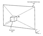
- FIG. 1 a shows an illuminator and its field of view
- FIG. 1 b shows a first illuminated region of interest
- FIG. 1 c shows a second illuminated region of interest
- FIG. 1 d shows scanning of an illuminated region of interest
- FIG. 1 e shows different sized illuminated regions of interest
- FIG. 2 a shows a side view of an illuminator capable of illuminating a region of interest and scanning the illuminated region of interest;
- FIG. 2 b shows a top down view of the illuminator of FIG. 2 a
- FIG. 3 a illustrates changing the size of the illuminated region of interest by adjusting the distance between a lens and a light source array
- FIG. 3 b illustrates that the direction of an emitted beam can be determined by adjusting the lateral offset of a lens with respect to a light source array
- FIG. 3 c illustrates that the direction of an emitted beam can be determined by tilting the angle of a lens
- FIG. 4 a shows a movable lens assembly for moving a lens vertically with respect to a light source array
- FIG. 4 b shows a movable lens assembly for moving a lens vertically and laterally with respect to a light source array
- FIG. 4 c shows a movable lens assembly for tilting a lens relative to a light source array
- FIG. 5 a shows an embodiment of an integrated camera having both traditional 2D image capture and 3D time-of-flight image capture functions
- FIG. 5 b shows a method performed by the system of FIG. 5 a
- FIG. 6 shows an embodiment of a computing system.
- a “smart illumination” time-of-flight system addresses some of the design challenges mentioned above.
- a “smart illumination” time-of-flight system can emit light on only a “region-of-interest” within the illuminator's field of view.
- the intensity of the emitted optical signal is strong enough to generate a detectable signal at the image sensor, while, at the same time, the illuminator's power consumption does not appreciably draw from the computer system's power supply.
- One smart illumination approach is to use a movable objective lens to collect and concentrate divergent light from an array of light sources into a more intense beam of light that can be directed to various regions of interest within the illuminator's field of view.
- an illuminator 101 possesses a field of view 102 over which it has the ability to shine light.
- the illuminator 101 may only direct light to a smaller region within the field of view 102 .
- the illuminated region can be directed to essentially any location within the field of view 102 .
- a challenge that “smart illumination” addresses is the desire to emit an optical signal having sufficient strength to generate a detectable signal at the image sensor, while, at the same time, avoiding excessive power consumption by the light source that generates the emitted light.
- One approach therefore, is to effectively reduce the natural emission angle of the physical light source(s) (e.g., LED(s) or laser(s)) by collecting and concentrating their divergent light through an objective lens to produce less divergent light (such as collimated or more focused light).
- the deliberate shaping of a less divergent emitted beam into a narrower beam effectively concentrates greater optical signal power onto a smaller region of interest 103 , 104 within the illuminator's field of view.
- smart illumination technology may “scan” the larger area with a smaller illuminated region.
- the illuminator may effectively illuminate region 105 by scanning a smaller sized illuminated region across area 105 .
- the illuminated region is centered at location 106
- the illuminated region is centered at location 107
- at time t 3 the illuminated region is centered at location 108
- at time t 4 the illuminated region is centered at location 109 .
- the illumination of larger sized region 105 can be comprehended even though a smaller sized illumination region was used.
- the size of the illuminated region 110 , 111 itself may be varied. Generally, larger illuminated region size may be tolerated commensurate with the extent to which weaker received signal strength at the sensor can be tolerated (e.g., the object of interest is closer to the illuminator, there is less conflicting ambient light, etc.) and/or the extent to which the system higher power consumption draw from the power supply can be tolerated.
- the larger the illuminated region the less scanning activity that would need to be performed by the illuminator to effectively illuminate a larger region of interest. Conceivably, some situations may permit a single illuminated region to be large enough to fill the entire field of view 102 .
- the illuminator 101 of FIG. 1 a concentrates the optical power from its light source(s) over a smaller region of illumination to boost received signal strength at the receiver. Because the illuminator 101 illuminates a smaller region, the illuminator is designed with the ability to move the smaller illuminated region to various locations within the field of view 102 . In some circumstances the illuminator 101 may scan the smaller illuminated region across a larger surface area to effectively illuminate the larger surface area. Additionally, the illuminator 101 may be designed to adjust the size of the illuminated region.
- Which region of the field of view is to be illuminated, what size the illuminated region is to have and whether or not any scanning is to be performed is a function of the particular condition/situation of the computing system and/or the particular application that it is executing.
- Examples of some situations/conditions/applications include, to name a few, intelligent recognition of a person's face (e.g., for secure access to the computing system) or intelligent recognition of the formation of a person's hand (e.g., for a user interface of the computing system that supports hand gesture recognition).
- the person's face or hand (“the object of interest”) is apt to consume only a portion of the field of view 102 .
- FIGS. 2 a and 2 b show different perspective views of an embodiment of an illuminator 201 having an objective lens 202 whose mechanical fixturing includes one or more electro-mechanical motors 203 that provide for movement of the objective lens 202 in various degrees of freedom (depending on implementation).
- a light source array 204 resides beneath the objective lens 202 . In operation, when the light sources of the light source array 204 are “on”, the light emitted by the light source array 204 is collected, shaped and directed by the lens 202 as a function of the positioning the lens 202 relative to the light source array 204 .
- the light source array 204 may be implemented, for example, as an array of light-emitted-diodes (LEDs) or lasers such as vertical cavity surface emitting lasers (VCSELs).
- LEDs light-emitted-diodes
- VCSELs vertical cavity surface emitting lasers
- the various light sources of the array are integrated on a same semiconductor chip substrate.
- the light sources of the array emit non-visible (e.g., infra-red (IR)) light so that the reflected time-of-flight signal does not interfere with the traditional visible light image capture function of the computing system.
- IR infra-red
- each of the light sources within the array may be connected to the same anode and same cathode so that all of the light sources within the array are either all on or all off (alternative embodiments could conceivably be designed to permit subsets of light sources within an array to be turned on/off together).
- An array of light sources tends to emit more uniform light than a single light source.
- each light source such as a single LED or VCSEL
- each light source by itself tends to emit non-uniform light. That is, the surface area of a region that is illuminated by a single LED or VCSEL will tend to have brighter spots and darker spots.
- emitted light from different devices tends to overlap resulting in dark spots from some light sources being irradiated by the bright spots of others. As such, the overall emitted light from the array tends to have a more uniform intensity profile.
- the illuminator may optionally include a diffuser 205 .
- Light is scattered as it propagates through the diffuser 205 resulting in more uniform light exiting the diffuser 205 than light entering the diffuser 205 .
- the diffuser 205 is depicted in FIG. 2 as being between the objective lens 202 and the exit port of the illuminator 201 , conceivably, the diffuser 205 may reside anywhere along the optical path of the illuminator 201 .
- the individual light sources typically have a wide emitted light divergence angle 206 .
- the wide divergence angle 206 of the individual light sources results in a wide divergence angle from the light source array 204 as a whole.
- the objective lens 202 collects the diverging light from the light source array 204 and forms a beam of emitted light 207 that is collimated or that is converging or at least has a smaller divergence angle.
- Collecting diverging light from the light source array 204 and forming a beam of more concentrated light increases the optical intensity per unit area of the emitted beam which, in turn, results in a stronger received signal at the sensor.
- the divergence angle 206 from the light source array is 60°, reducing the emitted beam's divergence angle to 30° will increase the signal strength at the sensor by a factor of 4.6. Reducing the emitted beam's divergence angle to 20° will increase the signal strength at the sensor by a factor of 10.7.
- Boosting received signal strength at the sensor through optical concentration of the emitted light from the light source array 204 preserves battery life as the light source array 204 will be able to sufficiently illuminate an object of interest without consuming significant amounts of power.
- FIGS. 3 a through 3 c provide some basic examples/embodiments of how the size and location of the illuminated region can be affected through manipulation of the positioning of the objective lens 202 .
- the size of the illuminated region 310 can be adjusted by varying the vertical distance 312 between the objective lens and the light source array.
- the objective lens forms a more collimated beam from a diverging light source.
- a wider radius of the diverging light is collected from the light source array by the lens resulting in an emitted beam shape having a wider width 310 .
- a smaller radius of the diverging light is collected from the light source array by the lens resulting in an emitted beam shape having a narrower width.
- Mechanical designs having electro-mechanical motorization for vertical lens movement as discussed just above with respect to FIG. 3 a are provided further below.
- the lens is placed closest to the light source array when the entire field of view is to be illuminated.
- the location of the illuminated region within the field of view can be adjusted by varying the horizontal location of the objective lens relative to the light source array.
- the position of the light source array is fixed and the objective lens is controllably moved along a plane 320 that resides parallel to and above the surface of the light source array.
- the greater the mis-alignment between the lens and light source array (as measured along plane 320 ), the greater the pointing angle of the emitted beam from the illuminator.
- the direction of the mis-alignment determines the pointing direction of the emitted beam. For example, as observed in FIG.
- misalignment in a first direction produces a beam that points along a first beam direction.
- misalignment in a second opposite direction as observed in FIG. 3 b ( ii ) produces a beam that points along a second beam direction that is opposite that of the first beam direction.
- the location of the illuminated region within the field of view can also be adjusted by varying the tilt angle of the objective lens. That is, tilting the lens will cause the beam to point in a direction that extends outward along the normal 330 from the outer surface of the lens.
- Mechanical designs having electro-mechanical motorization for inducing lens tilt as discussed just above with respect to FIG. 3 c are also provided further below.
- FIG. 4 a shows a more detailed movable lens assembly for adjusting the vertical distance of the objective lens 402 from the light source array 404 .
- a voice coil motor composed of a vertically movable inner member 410 with spring return 411 and hollow outer member 412 may be utilized where the objective lens 402 is housed within the vertically movable inner member 410 .
- the object lens 402 being fixed to the inner member 410 , moves vertically with the inner member 410 whose vertical position along the z axis is defined by the motor force applied by the inner member 410 against the return springs 411 .
- the motor force is defined by a voltage applied to the motor's coil.
- the coil is integrated with the inner member 410 and the outer member 412 includes a permanent magnet. A magnetic field responsive to a current driven through the coil interacts with the permanent magnet's magnetic field which determines the force applied to the inner member.
- voice-coil motors with spring return typically have a direct current-position relationship and therefore do not require a positioning sensor for feedback control.
- a housing surrounds the voice coil motor that the return springs compress 411 against as the inner member 410 extends higher along the z axis.
- the return springs may be underneath the motor and compress against the substrate that the light source array chip is mounted to. In this case, the diameter of the inner member should be greater than the width of the light source array semiconductor chip.
- FIG. 4 b shows a movable lens assembly for adjusting the lateral position of the object lens 402 relative to the light source array 404 .
- a pair of actuator voice coil motors 421 , 422 each with spring return 423 , 424 are used to define the position of the objective lens 402 in each of the x and y dimensions, respectively. That is, one voice coil motor 421 and return spring 423 establish the x position of the lens 402 and the other voice coil motor 422 and return spring 424 establish the y position of the lens 402 .
- the forces of the springs and motors are physically applied against the outer member 412 of the vertical member.
- the outer member 412 as depicted in FIG. 4 b has a cylindrical outer shape, in reality it may be square/rectangular so that the actuators 421 , 422 can apply a flush force against the outer member at off axis positions of the lens 402 .
- FIG. 4 c shows a movable lens assembly for adjusting the tilt angle of the lens.
- a pair of voice coil motors 431 , 432 each with spring return 433 , 434 are used as actuators to define the vertical position of each of two points along the outer edge of the lens 402 .
- the tilt angle of the lens 402 about the y axis is substantially defined by the force of a first motor 431 as applied against its return spring 433 .
- the tilt angle of the lens 402 about the x axis is substantially defined by the force of a first motor 432 as applied against its return spring 434 . From these basic scenarios, any tilt angle for the lens can be established as a function of the respective forces applied by the motors and the counteractive forces applied by the springs.
- the vertical positioning of the lens 402 can be established by actuating the two motors 431 , 432 equally. That is, if both motors 431 , 432 extend an equal amount outward the lens will be raised in the +z direction. Correspondingly, if both motors 431 , 432 recess an equal amount inward the lens will be lowered in the ⁇ z direction.
- One or more additional voice coil motor actuators may be located along the periphery of the lens holder to further stabilize both tilt angle and vertical positioning of the lens (e.g., three actuators spaced 120° apart, four actuators spaced 90° apart, etc.).
- voice-coil motors Although the discussion above has emphasized the use of voice-coil motors, other embodiments may use other devices such as piezoelectric actuators or stepper motors.
- FIG. 5 a shows an integrated traditional camera and time-of-flight imaging system 500 .
- the system has a connector 501 for making electrical contact, e.g., with a larger system/mother board, such as the system/mother board of a laptop computer, tablet computer or smartphone.
- the connector 501 may connect to a flex cable that, e.g., makes actual connection to the system/mother board or the connector 501 may make contact to the system/mother board directly.
- the connector 501 is affixed to a planar board 502 that may be implemented as a multi-layered structure of alternating conductive and insulating layers where the conductive layers are patterned to form electronic traces that support the internal electrical connections of the system 500 .
- the integrated RGBZ sensor 503 is mounted to the planar board 502 .
- the integrated RGBZ sensor includes different kinds of pixels, some of which are sensitive to visible light (e.g., a subset of R pixels that are sensitive to red visible blue light, a subset of G pixels that are sensitive to visible green light and a subset of B pixels that are sensitive to blue light) and others of which are sensitive to IR light.
- the RGB pixels are used to support traditional “2D” visible image capture (traditional picture taking) functions.
- the IR sensitive pixels are used to support 2D IR image capture and 3D depth profile imaging using time-of-flight techniques.
- RGB pixels for the visible image capture
- other embodiments may use different colored pixel schemes (e.g., Cyan, Magenta and Yellow).
- the integrated image sensor 503 may also include, for the IR sensitive pixels, special signaling lines or other circuitry to support time-of-flight detection including, e.g., clocking signal lines and/or other signal lines that indicate the timing of the reception of IR light (in view of the timing of the emission of the IR light from the light source array 505 ).
- special signaling lines or other circuitry to support time-of-flight detection including, e.g., clocking signal lines and/or other signal lines that indicate the timing of the reception of IR light (in view of the timing of the emission of the IR light from the light source array 505 ).
- the integrated image sensor 503 may also include a number or analog-to-digital converters (ADCs) to convert the analog signals received from the sensor's RGB pixels into digital data that is representative of the visible imagery in front of the camera lens module 504 .
- ADCs analog-to-digital converters
- the planar board 502 may likewise include signal traces to carry digital information provided by the ADCs to the connector 501 for processing by a higher end component of the computing system, such as an image signal processing pipeline (e.g., that is integrated on an applications processor).
- a camera lens module 504 is integrated above the integrated RGBZ image sensor 503 .
- the camera lens module 504 contains a system of one or more lenses to focus light received through an aperture onto the image sensor 503 .
- the camera lens module's reception of visible light may interfere with the reception of IR light by the image sensor's time-of-flight pixels, and, contra-wise, as the camera module's reception of IR light may interfere with the reception of visible light by the image sensor's RGB pixels
- either or both of the image sensor 503 and lens module 504 may contain a system of filters (e.g., filter 510 ) arranged to substantially block IR light that is to be received by RGB pixels, and, substantially block visible light that is to be received by time-of-flight pixels.
- filters e.g., filter 510
- An illuminator 507 composed of a light source array 505 beneath a movable objective lens 506 assembly is also mounted on the planar board 501 .
- the light source array 505 may be implemented on a semiconductor chip that is mounted to the planar board 501 . Embodiments of the light source array 505 and movable lens assembly 506 have been discussed above with respect to FIGS. 1 through 4 .
- the one or more supporting integrated circuits for the light source array may be mounted on the planar board 502 .
- the one or more integrated circuits may include LED or laser driver circuitry for driving respective currents through the light source array's light sources and coil driver circuitry for driving each of the coils associated with the voice coil motors of the movable lens assembly.
- Both the LED or laser driver circuitry and coil driver circuitry may include respective digital-to-analog circuitry to convert digital information received through connector 501 into a specific current drive strength for the light sources or a voice coil.
- the laser driver may additionally including clocking circuitry to generate a clock signal or other signal having a sequence of 1s and 0s that, when driven through the light sources will cause the light sources to repeatedly turn on and off so that the depth measurements can repeatedly be made.
- the integrated system 500 of FIG. 5 a supports three modes of operation: 1) 2D mode; 3) 3D mode; and, 3) 2D/3D mode.
- 2D mode the system behaves as a traditional camera.
- illuminator 507 is disabled and the image sensor is used to receive visible images through its RGB pixels.
- 3D mode the system is capturing time-of-flight depth information of an object in the field of view of the illuminator 507 and the camera lens module 504 .
- the illuminator is enabled and emitting IR light (e.g., in an on-off-on-off . . . sequence) onto the object.
- the IR light is reflected from the object, received through the camera lens module 504 and sensed by the image sensor's time-of-flight pixels.
- 2D/3D mode both the 2D and 3D modes described above are concurrently active.
- FIG. 5 b shows a method 500 that can be performed by the system of FIG. 5 a .
- the system drives current through a light source array to cause light to be emitted from the light source array 551 .
- the system collects and concentrates the light with a lens to form an emitted beam of light 552 .
- the system moves the lens to direct the beam of light to a region of interest to form an illuminated region of interest within a field of view, where, the size of the illuminated region of interest is smaller than the field of view 553 .
- the system detects at least a portion of the light after it has been reflected from an object of interest within the field of view and compares respective arrival times of the light against emission times of the light to generate depth information of the object of interest.
- FIG. 6 shows a depiction of an exemplary computing system 600 such as a personal computing system (e.g., desktop or laptop) or a mobile or handheld computing system such as a tablet device or smartphone.
- the basic computing system may include a central processing unit 601 (which may include, e.g., a plurality of general purpose processing cores 615 _ 1 through 615 _N and a main memory controller 617 disposed on an applications processor), system memory 602 , a display 603 (e.g., touchscreen, flat-panel), a local wired point-to-point link (e.g., USB) interface 604 , various network I/O functions 605 (such as an Ethernet interface and/or cellular modem subsystem), a wireless local area network (e.g., WiFi) interface 606 , a wireless point-to-point link (e.g., Bluetooth) interface 607 and a Global Positioning System interface 608 , various sensors 609 _ 1 through 609 _N, one
- An applications processor or multi-core processor 650 may include one or more general purpose processing cores 615 within its CPU 601 , one or more graphical processing units 616 , a memory management function 617 (e.g., a memory controller), an I/O control function 618 and one or more image signal processor pipelines 619 .
- the general purpose processing cores 615 typically execute the operating system and application software of the computing system.
- the graphics processing units 616 typically execute graphics intensive functions to, e.g., generate graphics information that is presented on the display 603 .
- the memory control function 617 interfaces with the system memory 602 to write/read data to/from system memory 602 .
- the image signal processing pipelines 619 receive image information from the camera 610 and process the raw image information for downstream uses.
- the power management control unit 612 generally controls the power consumption of the system 600 .
- Each of the touchscreen display 603 , the communication interfaces 604 - 607 , the GPS interface 608 , the sensors 609 , the camera 610 , and the speaker/microphone codec 613 , 614 all can be viewed as various forms of I/O (input and/or output) relative to the overall computing system including, where appropriate, an integrated peripheral device as well (e.g., the one or more cameras 610 ).
- I/O components may be integrated on the applications processor/multi-core processor 650 or may be located off the die or outside the package of the applications processor/multi-core processor 650 .
- one or more cameras 610 includes an integrated traditional visible image capture and time-of-flight depth measurement system such as the system 500 described above with respect to FIG. 5 .
- Application software, operating system software, device driver software and/or firmware executing on a general purpose CPU core (or other functional block having an instruction execution pipeline to execute program code) of an applications processor or other processor may direct commands to and receive image data from the camera system.
- commands may include entrance into or exit from any of the 2D, 3D or 2D/3D system states discussed above with respect to FIG. 5 . Additionally, commands may be directed to the movable lens sub-assembly of the illuminator to specify specific pointing directions of the movable lens, distance of the lens from the light source array (to specify illuminated region size) and a series of pointing directions of the movable lens to effect the aforementioned scanning of the aforementioned lens.
- Embodiments of the invention may include various processes as set forth above.
- the processes may be embodied in machine-executable instructions.
- the instructions can be used to cause a general-purpose or special-purpose processor to perform certain processes.
- these processes may be performed by specific hardware components that contain hardwired logic for performing the processes, or by any combination of programmed computer components and custom hardware components.
- Elements of the present invention may also be provided as a machine-readable medium for storing the machine-executable instructions.
- the machine-readable medium may include, but is not limited to, floppy diskettes, optical disks, CD-ROMs, and magneto-optical disks, FLASH memory, ROMs, RAMs, EPROMs, EEPROMs, magnetic or optical cards, propagation media or other type of media/machine-readable medium suitable for storing electronic instructions.
- the present invention may be downloaded as a computer program which may be transferred from a remote computer (e.g., a server) to a requesting computer (e.g., a client) by way of data signals embodied in a carrier wave or other propagation medium via a communication link (e.g., a modem or network connection).
- a remote computer e.g., a server
- a requesting computer e.g., a client
- a communication link e.g., a modem or network connection
Landscapes
- Engineering & Computer Science (AREA)
- Physics & Mathematics (AREA)
- Multimedia (AREA)
- Signal Processing (AREA)
- Radar, Positioning & Navigation (AREA)
- General Physics & Mathematics (AREA)
- Computer Networks & Wireless Communication (AREA)
- Remote Sensing (AREA)
- Electromagnetism (AREA)
- Human Computer Interaction (AREA)
- Computer Vision & Pattern Recognition (AREA)
- Length Measuring Devices By Optical Means (AREA)
- Stereoscopic And Panoramic Photography (AREA)
Priority Applications (6)
| Application Number | Priority Date | Filing Date | Title |
|---|---|---|---|
| US14/579,587 US9918073B2 (en) | 2014-12-22 | 2014-12-22 | Integrated camera system having two dimensional image capture and three dimensional time-of-flight capture with movable illuminated region of interest |
| EP15873921.9A EP3238432B1 (fr) | 2014-12-22 | 2015-11-17 | Système de caméra intégré ayant une capture d'image en deux dimensions et une capture de temps de vol en trois dimensions, avec région d'intérêt éclairée mobile |
| PCT/US2015/061060 WO2016105700A1 (fr) | 2014-12-22 | 2015-11-17 | Système de caméra intégré ayant une capture d'image en deux dimensions et une capture de temps de vol en trois dimensions, avec région d'intérêt éclairée mobile |
| DE112015005711.0T DE112015005711T5 (de) | 2014-12-22 | 2015-11-17 | Integriertes kamerasystem mit zweidimensionaler bilderfassung und dreidimensionaler laufzeiterfassung mit beweglicher beleuchteter region von interesse |
| CN201580035282.1A CN106489265B (zh) | 2014-12-22 | 2015-11-17 | 图像捕捉装置及计算系统 |
| GB1621167.4A GB2548666B (en) | 2014-12-22 | 2015-11-17 | Integrated camera system having two dimensional image capture and three dimensional time-of-flight capture with movable illuminated region of interest |
Applications Claiming Priority (1)
| Application Number | Priority Date | Filing Date | Title |
|---|---|---|---|
| US14/579,587 US9918073B2 (en) | 2014-12-22 | 2014-12-22 | Integrated camera system having two dimensional image capture and three dimensional time-of-flight capture with movable illuminated region of interest |
Publications (2)
| Publication Number | Publication Date |
|---|---|
| US20160182895A1 US20160182895A1 (en) | 2016-06-23 |
| US9918073B2 true US9918073B2 (en) | 2018-03-13 |
Family
ID=56131029
Family Applications (1)
| Application Number | Title | Priority Date | Filing Date |
|---|---|---|---|
| US14/579,587 Expired - Fee Related US9918073B2 (en) | 2014-12-22 | 2014-12-22 | Integrated camera system having two dimensional image capture and three dimensional time-of-flight capture with movable illuminated region of interest |
Country Status (6)
| Country | Link |
|---|---|
| US (1) | US9918073B2 (fr) |
| EP (1) | EP3238432B1 (fr) |
| CN (1) | CN106489265B (fr) |
| DE (1) | DE112015005711T5 (fr) |
| GB (1) | GB2548666B (fr) |
| WO (1) | WO2016105700A1 (fr) |
Cited By (4)
| Publication number | Priority date | Publication date | Assignee | Title |
|---|---|---|---|---|
| US10942362B2 (en) * | 2018-10-02 | 2021-03-09 | Himax Technologies Limited | Projector, electronic device having projector, and method for obtaining depth information of image data |
| US20230008801A1 (en) * | 2021-07-12 | 2023-01-12 | Seagate Technology Llc | Increased lidar aperture with refractive optical element |
| US20240069180A1 (en) * | 2021-06-23 | 2024-02-29 | Denso Corporation | Optical axis adjustment method, laser radar device, and optical axis adjustment system |
| US12196888B2 (en) | 2019-03-22 | 2025-01-14 | Viavi Solutions Inc. | Time of flight-based three-dimensional sensing system |
Families Citing this family (28)
| Publication number | Priority date | Publication date | Assignee | Title |
|---|---|---|---|---|
| US9992396B1 (en) * | 2015-02-02 | 2018-06-05 | Apple Inc. | Focusing lighting module |
| CN108369364B (zh) | 2015-11-10 | 2021-07-16 | 亮锐控股有限公司 | 自适应光源 |
| CN106534831A (zh) * | 2016-11-15 | 2017-03-22 | 上海传英信息技术有限公司 | 立体视频拍摄方法及用户终端 |
| US10917626B2 (en) | 2016-11-23 | 2021-02-09 | Microsoft Technology Licensing, Llc | Active illumination 3D imaging system |
| US10598771B2 (en) * | 2017-01-18 | 2020-03-24 | Analog Devices Global Unlimited Company | Depth sensing with multiple light sources |
| US10542245B2 (en) * | 2017-05-24 | 2020-01-21 | Lg Electronics Inc. | Mobile terminal and method for controlling the same |
| US10901073B2 (en) | 2017-07-11 | 2021-01-26 | Microsoft Technology Licensing, Llc | Illumination for zoned time-of-flight imaging |
| US10430958B2 (en) | 2017-07-11 | 2019-10-01 | Microsoft Technology Licensing, Llc | Active illumination 3D zonal imaging system |
| CN107706703B (zh) * | 2017-09-30 | 2019-07-26 | 维沃移动通信有限公司 | 一种激光光路控制方法、装置和移动终端 |
| GB2579689A (en) * | 2018-08-07 | 2020-07-01 | Cambridge Mechatronics Ltd | Improved 3D sensing |
| CN109120758A (zh) * | 2018-10-09 | 2019-01-01 | Oppo广东移动通信有限公司 | 光线发射器、飞行时间模组以及电子设备 |
| WO2020154070A1 (fr) * | 2019-01-23 | 2020-07-30 | Microsoft Technology Licensing, Llc | Éclairage destiné à une imagerie de temps de vol zonée |
| US20200344405A1 (en) * | 2019-04-25 | 2020-10-29 | Canon Kabushiki Kaisha | Image pickup apparatus of measuring distance from subject to image pickup surface of image pickup device and method for controlling the same |
| KR20220003600A (ko) * | 2019-05-30 | 2022-01-10 | 옵시스 테크 엘티디 | 액추에이터를 사용하는 눈-안전 장거리 lidar 시스템 |
| US20220229189A1 (en) * | 2019-07-05 | 2022-07-21 | Sony Semiconductor Solutions Corporation | Time-of-flight sensor and system |
| GB2585952A (en) * | 2019-07-26 | 2021-01-27 | Cambridge Mechatronics Ltd | Method |
| JP2021025965A (ja) * | 2019-08-08 | 2021-02-22 | 富士ゼロックス株式会社 | 発光装置、光学装置及び情報処理装置 |
| GB2588678A (en) * | 2019-11-01 | 2021-05-05 | Cambridge Mechatronics Ltd | A time-of-flight sensor system |
| CA3165230C (fr) * | 2019-12-30 | 2025-07-22 | Matterport, Inc. | Systeme et procede de capture et de generation d'images panoramiques tridimensionnelles |
| US11888289B2 (en) * | 2020-03-30 | 2024-01-30 | Namuga, Co., Ltd. | Light source module allowing differential control according to distance to subject and method for controlling the same |
| WO2021208041A1 (fr) * | 2020-04-16 | 2021-10-21 | 华为技术有限公司 | Ensemble électroluminescent, module de caméra de temps de vol et terminal mobile |
| WO2021248427A1 (fr) * | 2020-06-12 | 2021-12-16 | 深圳市汇顶科技股份有限公司 | Dispositif de détection de profondeur et dispositif électronique associé, et procédé de fonctionnement de dispositif de détection de profondeur |
| KR102473423B1 (ko) * | 2021-05-03 | 2022-12-02 | 삼성전기주식회사 | Tof 카메라 장치 |
| CN115542287A (zh) * | 2021-06-29 | 2022-12-30 | 北京小米移动软件有限公司 | 激光发射模块、深度相机及电子设备 |
| US20250180715A1 (en) * | 2021-07-06 | 2025-06-05 | Sony Semiconductor Solutions Corporation | Light receiving device, distance measuring device, and method for controlling light receiving device |
| JP7800172B2 (ja) * | 2022-02-02 | 2026-01-16 | 富士フイルムビジネスイノベーション株式会社 | 距離測定装置及び距離測定プログラム |
| US12363410B2 (en) * | 2022-02-04 | 2025-07-15 | Lumileds Llc | Parallax correction for illumination system and method |
| WO2024135531A1 (fr) * | 2022-12-19 | 2024-06-27 | アルプスアルパイン株式会社 | Dispositif d'entraînement d'élément optique et système de mesure de distance |
Citations (37)
| Publication number | Priority date | Publication date | Assignee | Title |
|---|---|---|---|---|
| US6157387A (en) | 1997-06-02 | 2000-12-05 | Nippon Telegraph And Telephone Corporation | Image generating apparatus and method |
| US20040114921A1 (en) * | 1999-02-16 | 2004-06-17 | Braun Ori J. | Method and apparatus for providing adaptive illumination |
| US20070236582A1 (en) | 2006-03-29 | 2007-10-11 | Imaging Solutions Group Of Ny, Inc. | Video camera with multiple independent outputs |
| US7560679B1 (en) | 2005-05-10 | 2009-07-14 | Siimpel, Inc. | 3D camera |
| US7936038B2 (en) | 2009-03-27 | 2011-05-03 | Samsung Electro-Mechanics Co. | Photodiode cell structure of photodiode integrated circuit for optical pickup and method of manufacturing the same |
| KR20110064622A (ko) | 2009-12-08 | 2011-06-15 | 삼성전자주식회사 | 티오에프 카메라를 이용한 3차원 에지 추출 방법 및 장치 |
| US7990636B2 (en) | 2009-12-18 | 2011-08-02 | Samsung Electro-Mechanics Co., Ltd. | Lens actuating module |
| US20110194007A1 (en) | 2010-02-05 | 2011-08-11 | Byung Hoon Kim | Cmos image sensor |
| US8027107B2 (en) | 2009-08-18 | 2011-09-27 | Samsung Electro-Mechanics Co., Ltd. | Camera module |
| US20110242115A1 (en) | 2010-03-30 | 2011-10-06 | You-Ming Tsao | Method for performing image signal processing with aid of a graphics processing unit, and associated apparatus |
| US20120033857A1 (en) | 2008-10-10 | 2012-02-09 | Alain Bergeron | Selective and adaptive illumination of a target |
| US8116018B2 (en) | 2009-09-11 | 2012-02-14 | Samsung Electro-Mechanics Co., Ltd. | Lens actuating module |
| US8134637B2 (en) | 2004-01-28 | 2012-03-13 | Microsoft Corporation | Method and system to increase X-Y resolution in a depth (Z) camera using red, blue, green (RGB) sensing |
| US8159016B2 (en) | 2003-12-15 | 2012-04-17 | Samsung Electronics Co., Ltd. | Capacitor of a semiconductor device |
| US8159762B2 (en) | 2009-10-19 | 2012-04-17 | Samsung Electro-Mechanics Co., Ltd. | Lens actuating module |
| US20120147235A1 (en) | 2010-12-14 | 2012-06-14 | Christopher Parks | Image sensor with charge multiplication |
| US8218016B2 (en) | 2009-11-10 | 2012-07-10 | Samsung Electro-Mechanics Co., Ltd | Image stabilization mechanism for camera module |
| US8320621B2 (en) | 2009-12-21 | 2012-11-27 | Microsoft Corporation | Depth projector system with integrated VCSEL array |
| US20130026859A1 (en) | 2011-07-29 | 2013-01-31 | Samsung Electro-Mechanics Co., Ltd. | Linear motor |
| US20130131836A1 (en) | 2011-11-21 | 2013-05-23 | Microsoft Corporation | System for controlling light enabled devices |
| US20130134470A1 (en) | 2011-11-28 | 2013-05-30 | Samsung Electro-Mechanics Co., Ltd. | Light emitting diode package module |
| US20130163627A1 (en) | 2011-12-24 | 2013-06-27 | Princeton Optronics | Laser Illuminator System |
| US20130188022A1 (en) | 2012-01-23 | 2013-07-25 | Microsoft Corporation | 3d zoom imager |
| US20130201292A1 (en) | 2010-04-16 | 2013-08-08 | Otto-Von Guericke-Universitat Magdeburg | Device For Monitoring At Least One Three-Dimensional Safety Area |
| US20130234029A1 (en) | 2012-03-06 | 2013-09-12 | Omnivision Technologies, Inc. | Image sensor for two-dimensional and three-dimensional image capture |
| US20130291414A1 (en) | 2011-09-29 | 2013-11-07 | Erik J. Cegnar | Light apparatuses and lighting systems |
| US20140028870A1 (en) | 2011-07-20 | 2014-01-30 | Broadcom Corporation | Concurrent image processing for generating an output image |
| US20140049610A1 (en) | 2012-08-14 | 2014-02-20 | Microsoft Corporation | Illumination light projection for a depth camera |
| US20140055771A1 (en) * | 2012-02-15 | 2014-02-27 | Mesa Imaging Ag | Time of Flight Camera with Stripe Illumination |
| KR20140028536A (ko) | 2012-08-29 | 2014-03-10 | 엘지전자 주식회사 | 깊이 영상 생성 장치 및 방법 |
| US20140152813A1 (en) | 2011-08-25 | 2014-06-05 | Ifm Electronic Gmbh | Time-of-flight camera with signal path monitoring |
| US20140160259A1 (en) | 2012-07-26 | 2014-06-12 | Olive Medical Corporation | Camera system with minimal area monolithic cmos image sensor |
| US8761594B1 (en) * | 2013-02-28 | 2014-06-24 | Apple Inc. | Spatially dynamic illumination for camera systems |
| US20140176663A1 (en) | 2012-12-20 | 2014-06-26 | Microsoft Corporation | Privacy camera |
| US20140211193A1 (en) | 2012-09-24 | 2014-07-31 | Alces Technology, Inc. | Structured light and time of flight depth capture with a MEMS ribbon linear array spatial light modulator |
| WO2014125272A1 (fr) | 2013-02-13 | 2014-08-21 | Light Blue Optics Ltd | Systèmes de détection de contact |
| US20150260830A1 (en) | 2013-07-12 | 2015-09-17 | Princeton Optronics Inc. | 2-D Planar VCSEL Source for 3-D Imaging |
Family Cites Families (4)
| Publication number | Priority date | Publication date | Assignee | Title |
|---|---|---|---|---|
| JP4712480B2 (ja) * | 2005-08-10 | 2011-06-29 | オリンパスイメージング株式会社 | レンズ駆動装置 |
| WO2007067296A2 (fr) * | 2005-12-02 | 2007-06-14 | Alis Corporation | Sources d'ions, systemes et procedes associes |
| WO2009040745A1 (fr) * | 2007-09-26 | 2009-04-02 | Koninklijke Philips Electronics N.V. | Unité d'entraînement d'objectif pour un dispositif optique |
| US8736818B2 (en) * | 2010-08-16 | 2014-05-27 | Ball Aerospace & Technologies Corp. | Electronically steered flash LIDAR |
-
2014
- 2014-12-22 US US14/579,587 patent/US9918073B2/en not_active Expired - Fee Related
-
2015
- 2015-11-17 CN CN201580035282.1A patent/CN106489265B/zh active Active
- 2015-11-17 EP EP15873921.9A patent/EP3238432B1/fr active Active
- 2015-11-17 GB GB1621167.4A patent/GB2548666B/en active Active
- 2015-11-17 WO PCT/US2015/061060 patent/WO2016105700A1/fr not_active Ceased
- 2015-11-17 DE DE112015005711.0T patent/DE112015005711T5/de not_active Ceased
Patent Citations (37)
| Publication number | Priority date | Publication date | Assignee | Title |
|---|---|---|---|---|
| US6157387A (en) | 1997-06-02 | 2000-12-05 | Nippon Telegraph And Telephone Corporation | Image generating apparatus and method |
| US20040114921A1 (en) * | 1999-02-16 | 2004-06-17 | Braun Ori J. | Method and apparatus for providing adaptive illumination |
| US8159016B2 (en) | 2003-12-15 | 2012-04-17 | Samsung Electronics Co., Ltd. | Capacitor of a semiconductor device |
| US8134637B2 (en) | 2004-01-28 | 2012-03-13 | Microsoft Corporation | Method and system to increase X-Y resolution in a depth (Z) camera using red, blue, green (RGB) sensing |
| US7560679B1 (en) | 2005-05-10 | 2009-07-14 | Siimpel, Inc. | 3D camera |
| US20070236582A1 (en) | 2006-03-29 | 2007-10-11 | Imaging Solutions Group Of Ny, Inc. | Video camera with multiple independent outputs |
| US20120033857A1 (en) | 2008-10-10 | 2012-02-09 | Alain Bergeron | Selective and adaptive illumination of a target |
| US7936038B2 (en) | 2009-03-27 | 2011-05-03 | Samsung Electro-Mechanics Co. | Photodiode cell structure of photodiode integrated circuit for optical pickup and method of manufacturing the same |
| US8027107B2 (en) | 2009-08-18 | 2011-09-27 | Samsung Electro-Mechanics Co., Ltd. | Camera module |
| US8116018B2 (en) | 2009-09-11 | 2012-02-14 | Samsung Electro-Mechanics Co., Ltd. | Lens actuating module |
| US8159762B2 (en) | 2009-10-19 | 2012-04-17 | Samsung Electro-Mechanics Co., Ltd. | Lens actuating module |
| US8218016B2 (en) | 2009-11-10 | 2012-07-10 | Samsung Electro-Mechanics Co., Ltd | Image stabilization mechanism for camera module |
| KR20110064622A (ko) | 2009-12-08 | 2011-06-15 | 삼성전자주식회사 | 티오에프 카메라를 이용한 3차원 에지 추출 방법 및 장치 |
| US7990636B2 (en) | 2009-12-18 | 2011-08-02 | Samsung Electro-Mechanics Co., Ltd. | Lens actuating module |
| US8320621B2 (en) | 2009-12-21 | 2012-11-27 | Microsoft Corporation | Depth projector system with integrated VCSEL array |
| US20110194007A1 (en) | 2010-02-05 | 2011-08-11 | Byung Hoon Kim | Cmos image sensor |
| US20110242115A1 (en) | 2010-03-30 | 2011-10-06 | You-Ming Tsao | Method for performing image signal processing with aid of a graphics processing unit, and associated apparatus |
| US20130201292A1 (en) | 2010-04-16 | 2013-08-08 | Otto-Von Guericke-Universitat Magdeburg | Device For Monitoring At Least One Three-Dimensional Safety Area |
| US20120147235A1 (en) | 2010-12-14 | 2012-06-14 | Christopher Parks | Image sensor with charge multiplication |
| US20140028870A1 (en) | 2011-07-20 | 2014-01-30 | Broadcom Corporation | Concurrent image processing for generating an output image |
| US20130026859A1 (en) | 2011-07-29 | 2013-01-31 | Samsung Electro-Mechanics Co., Ltd. | Linear motor |
| US20140152813A1 (en) | 2011-08-25 | 2014-06-05 | Ifm Electronic Gmbh | Time-of-flight camera with signal path monitoring |
| US20130291414A1 (en) | 2011-09-29 | 2013-11-07 | Erik J. Cegnar | Light apparatuses and lighting systems |
| US20130131836A1 (en) | 2011-11-21 | 2013-05-23 | Microsoft Corporation | System for controlling light enabled devices |
| US20130134470A1 (en) | 2011-11-28 | 2013-05-30 | Samsung Electro-Mechanics Co., Ltd. | Light emitting diode package module |
| US20130163627A1 (en) | 2011-12-24 | 2013-06-27 | Princeton Optronics | Laser Illuminator System |
| US20130188022A1 (en) | 2012-01-23 | 2013-07-25 | Microsoft Corporation | 3d zoom imager |
| US20140055771A1 (en) * | 2012-02-15 | 2014-02-27 | Mesa Imaging Ag | Time of Flight Camera with Stripe Illumination |
| US20130234029A1 (en) | 2012-03-06 | 2013-09-12 | Omnivision Technologies, Inc. | Image sensor for two-dimensional and three-dimensional image capture |
| US20140160259A1 (en) | 2012-07-26 | 2014-06-12 | Olive Medical Corporation | Camera system with minimal area monolithic cmos image sensor |
| US20140049610A1 (en) | 2012-08-14 | 2014-02-20 | Microsoft Corporation | Illumination light projection for a depth camera |
| KR20140028536A (ko) | 2012-08-29 | 2014-03-10 | 엘지전자 주식회사 | 깊이 영상 생성 장치 및 방법 |
| US20140211193A1 (en) | 2012-09-24 | 2014-07-31 | Alces Technology, Inc. | Structured light and time of flight depth capture with a MEMS ribbon linear array spatial light modulator |
| US20140176663A1 (en) | 2012-12-20 | 2014-06-26 | Microsoft Corporation | Privacy camera |
| WO2014125272A1 (fr) | 2013-02-13 | 2014-08-21 | Light Blue Optics Ltd | Systèmes de détection de contact |
| US8761594B1 (en) * | 2013-02-28 | 2014-06-24 | Apple Inc. | Spatially dynamic illumination for camera systems |
| US20150260830A1 (en) | 2013-07-12 | 2015-09-17 | Princeton Optronics Inc. | 2-D Planar VCSEL Source for 3-D Imaging |
Non-Patent Citations (6)
| Title |
|---|
| International Preliminary Report on Patentability, issued in International Application No. PCT/2015/058646, dated Jun. 27, 2017, 9 pages. |
| International Search Report and Written Opinion issued in International Application No. PCT/US2015/062157, dated Mar. 8, 2016, 12 pages. |
| PCT/US2015/058646-International Search Report and Written Opinion, dated Mar. 3, 2016, 13 pages. |
| PCT/US2015/058646—International Search Report and Written Opinion, dated Mar. 3, 2016, 13 pages. |
| PCT/US2015/061060-International Search Report and Written Opinion, dated Feb. 24, 2016, 9 pages. |
| PCT/US2015/061060—International Search Report and Written Opinion, dated Feb. 24, 2016, 9 pages. |
Cited By (4)
| Publication number | Priority date | Publication date | Assignee | Title |
|---|---|---|---|---|
| US10942362B2 (en) * | 2018-10-02 | 2021-03-09 | Himax Technologies Limited | Projector, electronic device having projector, and method for obtaining depth information of image data |
| US12196888B2 (en) | 2019-03-22 | 2025-01-14 | Viavi Solutions Inc. | Time of flight-based three-dimensional sensing system |
| US20240069180A1 (en) * | 2021-06-23 | 2024-02-29 | Denso Corporation | Optical axis adjustment method, laser radar device, and optical axis adjustment system |
| US20230008801A1 (en) * | 2021-07-12 | 2023-01-12 | Seagate Technology Llc | Increased lidar aperture with refractive optical element |
Also Published As
| Publication number | Publication date |
|---|---|
| EP3238432A1 (fr) | 2017-11-01 |
| EP3238432A4 (fr) | 2018-08-01 |
| US20160182895A1 (en) | 2016-06-23 |
| WO2016105700A1 (fr) | 2016-06-30 |
| GB2548666A (en) | 2017-09-27 |
| GB201621167D0 (en) | 2017-01-25 |
| DE112015005711T5 (de) | 2017-11-02 |
| EP3238432B1 (fr) | 2023-04-19 |
| CN106489265A (zh) | 2017-03-08 |
| GB2548666B (en) | 2021-06-23 |
| CN106489265B (zh) | 2019-07-05 |
Similar Documents
| Publication | Publication Date | Title |
|---|---|---|
| US9918073B2 (en) | Integrated camera system having two dimensional image capture and three dimensional time-of-flight capture with movable illuminated region of interest | |
| US10306209B2 (en) | Illuminator for camera system having three dimensional time-of-flight capture with movable mirror element | |
| US10055854B2 (en) | Time-of-flight camera system and method to improve measurement quality of weak field-of-view signal regions | |
| US9832357B2 (en) | Time-of-flight camera system with scanning iluminator | |
| US20170374355A1 (en) | Integrated Camera System Having Two Dimensional Image Capture and Three Dimensional Time-of-Flight Capture With A Partitioned Field of View | |
| US20160178991A1 (en) | Smart illumination time of flight system and method | |
| US9918024B2 (en) | Multi functional camera with beam splitter | |
| US20170370702A1 (en) | Multi Functional Camera With Multiple Reflection Beam Splitter |
Legal Events
| Date | Code | Title | Description |
|---|---|---|---|
| AS | Assignment |
Owner name: GOOGLE INC., CALIFORNIA Free format text: ASSIGNMENT OF ASSIGNORS INTEREST;ASSIGNORS:KO, JAMYUEN;WAN, CHUNG CHAN;REEL/FRAME:034570/0890 Effective date: 20141218 |
|
| AS | Assignment |
Owner name: GOOGLE LLC, CALIFORNIA Free format text: CHANGE OF NAME;ASSIGNOR:GOOGLE INC.;REEL/FRAME:044129/0001 Effective date: 20170929 |
|
| STCF | Information on status: patent grant |
Free format text: PATENTED CASE |
|
| MAFP | Maintenance fee payment |
Free format text: PAYMENT OF MAINTENANCE FEE, 4TH YEAR, LARGE ENTITY (ORIGINAL EVENT CODE: M1551); ENTITY STATUS OF PATENT OWNER: LARGE ENTITY Year of fee payment: 4 |
|
| FEPP | Fee payment procedure |
Free format text: MAINTENANCE FEE REMINDER MAILED (ORIGINAL EVENT CODE: REM.); ENTITY STATUS OF PATENT OWNER: LARGE ENTITY |
|
| LAPS | Lapse for failure to pay maintenance fees |
Free format text: PATENT EXPIRED FOR FAILURE TO PAY MAINTENANCE FEES (ORIGINAL EVENT CODE: EXP.); ENTITY STATUS OF PATENT OWNER: LARGE ENTITY |
|
| STCH | Information on status: patent discontinuation |
Free format text: PATENT EXPIRED DUE TO NONPAYMENT OF MAINTENANCE FEES UNDER 37 CFR 1.362 |